
Разметка печатной платы

Altium Essentials: PCB Introduction
This content is part of the official Altium Professional Training Program. For full courses, materials and certification, visit Altium Training.
Внутри каждого электронного изделия находится печатная плата, или PCB. Сегодня компоненты настолько уменьшились, что их размеры измеряются долями миллиметра, а не сантиметрами, а ширина дорожек сократилась с 10 mil — широких, хорошо разнесенных линий — до тонких, словно волос, линий шириной 2–3 mil, плотно расположенных друг к другу. Рост скоростей сигналов также привел к тому, что межсоединения на PCB перестали быть просто медными проводниками, передающими электрическую энергию, и стали вести себя как высокоскоростные линии передачи, что требует соответствующих методов проектирования. Механические требования тоже стали более сложными. Компактные современные электронные устройства необычной формы требуют компактных печатных плат необычной формы, которые часто выполняются в виде rigid-flex конструкций — такие платы могут иметь изогнутые края и вырезы, что требует тщательно продуманного размещения компонентов.
Эти задачи можно решить с помощью технологий проектирования PCB от Altium. Редактор PCB в Altium Designer позволяет создавать, редактировать и проверять ваши проекты PCB.
Настройка редактора PCB
Категория PCB Editor в диалоговом окне Preferences (открывается щелчком по значку ![]() в правом верхнем углу рабочей области) предоставляет доступ к страницам настроек, влияющих на поведение редактора PCB. К этим настройкам можно обращаться в любой момент, чтобы конфигурировать параметры по мере необходимости.
в правом верхнем углу рабочей области) предоставляет доступ к страницам настроек, влияющих на поведение редактора PCB. К этим настройкам можно обращаться в любой момент, чтобы конфигурировать параметры по мере необходимости.

Используйте категорию PCB Editor в Preferences Altium Designer для настройки редактора PCB.
Подробнее о настройках PCB: PCB Editor Preferences.
Настройка документа PCB
Чтобы начать трассировку вашей PCB, добавьте новый документ PCB в проект PCB. Для этого щелкните правой кнопкой мыши по записи проекта на панели Projects и выберите команду Add New to Project » PCB в контекстном меню. Стандартный документ PCB появится в рабочей области.

Новый созданный документ PCB станет активным документом в рабочей области.
Параметры документа PCB настраиваются на панели Properties, когда в рабочей области не выбран ни один объект. Основные параметры настраиваются на вкладке General этой панели:
-
Настройка сетки (область Grid Manager) — настройте параметры глобальной сетки по умолчанию или добавьте дополнительные сетки (декартовы и полярные) по мере необходимости. Сетки обеспечивают точное перемещение и размещение объектов.
- Единицы измерения (область Other) — выберите предпочтительные единицы измерения (mm или mils) для документа.

Настройте параметры документа PCB на панели Properties.
Подробнее о настройке документа PCB: PCB Environment Setup.
Задание формы платы и начала координат
Форма платы, также называемая контуром платы, определяет общие габариты платы. По умолчанию плата представляет собой прямоугольник размером 6000 x 4000 mil (152,4 x 101,6 мм). Редактор PCB предоставляет ряд инструментов для задания требуемой формы платы.
Вы можете интерактивно задать новую форму платы следующим образом:
-
Перейдите в режим Board Planning Mode редактора, выбрав команду View » Board Planning Mode в главном меню.
-
Выберите команду Design » Redefine Board Shape в главном меню.
-
Установите курсор и щелкните, чтобы зафиксировать начальную вершину формы платы.
-
Переместите курсор для размещения второй вершины и щелкните, чтобы установить ее.
-
Продолжайте перемещать мышь и щелкать для размещения следующих вершин.
-
После размещения последней вершины щелкните правой кнопкой мыши, чтобы замкнуть и завершить определение формы платы. Нет необходимости замыкать форму вручную, так как редактор PCB автоматически завершит форму, соединив начальную точку с последней размещенной точкой.
Также можно редактировать существующую форму вместо ее повторного задания следующим образом:
- Перейдите в режим Board Planning Mode редактора, выбрав команду View » Board Planning Mode в главном меню.
- Выберите команду Design » Edit Board Shape в главном меню.
-
Щелкните, удерживайте и перетащите сторону или вершину формы платы, чтобы переместить ее.
- Выйдите из режима редактирования, щелкнув в любом месте рабочей области (по контуру платы или вне его).
Используйте команду View » 2D Layout Mode в главном меню, чтобы вернуться в режим 2D Layout Mode редактора.
Подробнее о доступных методах задания формы платы: Defining the Board Shape.
Настройка отображения слоев
Помимо слоев, используемых для изготовления платы, включая сигнальные слои, слои плоскостей питания, маски и шелкографии, редактор PCB также поддерживает множество других неэлектрических слоев. Слои часто группируются следующим образом:
-
Electrical Layers – включает 128 сигнальных слоев и 16 внутренних слоев плоскостей питания.
-
Component Layers – слои, используемые при проектировании компонентов, включая слои Overlay (шелкография), Solder и Paste. Если объект размещен в посадочном месте компонента на одном из этих слоев в редакторе библиотек, то при переворачивании компонента с верхней стороны платы на нижнюю все объекты, обнаруженные на слое Component, будут перенесены на соответствующий парный слой Component. Это также включает объекты на определяемых пользователем парах слоев Component Layer Pairs (спаренных механических слоях).
-
Mechanical Layers – программное обеспечение поддерживает неограниченное количество механических слоев общего назначения, которые используются для таких задач проектирования, как размеры, данные для изготовления, инструкции по сборке и т. д. Эти слои при необходимости можно выборочно включать в печать и генерацию Gerber-файлов. Механические слои также могут быть спаренными; если они спарены, они ведут себя как слои Component Layers. Спаренные Component Layers используются для таких задач, как размещение 3D-тел, клеевых точек и выборочного золочения краевых разъемов.
-
Other Layers – к ним относятся слой Keep-Out (используется для задания запретных зон, действующих на всех медных слоях), multi-layer (используется для объектов, присутствующих на всех сигнальных слоях, например контактных площадок и переходных отверстий), слой Drill Drawing (используется для размещения информации о сверлении, например таблицы отверстий) и слой Drill Guide (используется для отображения маркеров, указывающих расположение и размеры отверстий).
Медные слои добавляются в проект и удаляются из него в Layer Stack Manager, который рассматривается в следующем разделе. Все остальные слои включаются и настраиваются на панели View Configuration.


Две вкладки панели View Configuration
Помимо состояния отображения слоев и настроек цветов, панель View Configuration также предоставляет доступ к другим параметрам отображения, включая:
-
Цвет и видимость System Colors, например цвет выделения или отображение Connection Lines.
-
Способ отображения каждого типа объектов (сплошной или черновой), а также их прозрачность (раздел Object Visibility).
-
Различные параметры вида, например следует ли отображать Origin Marker, имена Pad Net и Pad Numbers (раздел Additional Options).
-
Степень затемнения отображения, когда объекты приглушены или замаскированы (раздел Mask and Dim Settings).
-
Создание наборов слоев Layer Sets, которые обеспечивают быстрый способ переключения видимых в данный момент слоев с помощью элемента управления
 (раздел Layers).
-
Создание и выбор конфигураций вида View Configurations, которые используются для предварительной настройки всех свойств слоев, таких как цвет, видимость, прозрачность объектов и т. д. (раздел General Settings).
Несколько замечаний о слоях:
-
Текущие включенные слои показаны в виде ряда вкладок в нижней части рабочей области проектирования PCB, как показано на изображении ниже. Щелкните правой кнопкой мыши по вкладке, чтобы получить доступ к часто используемым командам отображения слоев.

-
При размещении объектов на PCB следует учитывать, на каком слое они будут размещены. Объекты размещаются на текущем слое, который показан как активная вкладка слоя в нижней части рабочей области. На изображении выше активным слоем является Top Layer.
-
Чтобы переключить активный слой:
-
Щелкните вкладку слоя в нижней части рабочей области, или
-
Нажимайте цифровые клавиши + или -, чтобы циклически переключаться между всеми слоями, или
-
Нажимайте цифровую клавишу *, чтобы циклически переключаться между сигнальными слоями, или
-
Используйте сочетания клавиш Ctrl+Shift+Mouse Wheel.
-
-
В насыщенном проекте может быть полезно отображать только тот слой, с которым вы сейчас работаете; это называется Single Layer Mode. Чтобы включить или выключить режим отображения одного слоя, нажмите сочетание клавиш Shift+S. Параметры Available Single Layer Modes настраиваются на странице PCB Editor – Board Insight Display диалогового окна Preferences. Каждое нажатие Shift+S будет переключать на следующий включенный режим одного слоя.
Подробнее о настройке вида печатной платы: Ваше представление PCB.
Определение стека слоев
Печатная плата проектируется и формируется как стек слоев, определяемый в Layer Stack Manager (Design » Layer Stack Manager). Layer Stack Manager открывается в редакторе документов так же, как лист схемы, PCB и другие типы документов. Функциональность разделена между вкладками, отображаемыми в нижней части Layer Stack Manager. Основные операции настройки выполняются на вкладках Stackup и Via Types.
На вкладке Stackup приводятся данные о производственных слоях. На этой вкладке можно добавлять, удалять и настраивать слои.
|
Чтобы добавить слой, выберите в области таблицы слой, над или под которым нужно добавить новый слой, нажмите кнопку Add в верхней части Layer Stack Manager и воспользуйтесь появившимся всплывающим меню. Чтобы удалить слой, выберите его в области таблицы и нажмите кнопку Delete. Чтобы выбрать материал слоя из библиотеки материалов, выберите нужный слой в области таблицы и нажмите кнопку Modify. Свойства, определенные для выбранного материала, будут применены к слою. Свойства текущего выбранного слоя также можно редактировать непосредственно в области таблицы или на панели Properties. |


Вкладка Via Types используется для определения допустимых требований к переходным отверстиям по охвату слоев в плоскости Z, используемым в проекте.
|
Тип переходного отверстия по умолчанию — сквозное — всегда присутствует в проекте PCB. Чтобы добавить дополнительный тип переходного отверстия (blind, buried или micro via), нажмите кнопку Add в верхней части Layer Stack Manager, а затем выберите слои, которые охватывает этот тип переходного отверстия, в раскрывающихся списках First layer и Last layer на панели Properties, когда тип переходного отверстия выбран в области таблицы. Чтобы удалить добавленный тип переходного отверстия, выберите его в области таблицы и нажмите кнопку Delete . |


Используйте команду File » Save to PCB в Layer Stack Manager, чтобы отразить изменения в PCB.
Подробнее о Layer Stack Manager: Определение стека слоев, Определение blind, buried и micro vias.
Настройка правил проектирования
Правила проектирования отслеживают и проверяют ваш проект на соответствие различным требованиям, таким как зазоры между медными объектами, ширина проводников, длины цепей и т. д. В совокупности правила проектирования образуют набор инструкций, которым должен следовать редактор PCB.
Правила проектирования определяются и управляются из диалогового окна PCB Rules and Constraints Editor, доступ к которому осуществляется через команду Design » Rules в главном меню.
Диалоговое окно PCB Rules and Constraints Editor содержит два раздела:
- В левой части диалогового окна отображается дерево, в котором перечислены доступные категории правил, типы правил в каждой категории и отдельные правила каждого типа, определенные в данный момент.
- В правой части диалогового окна отображается информация, относящаяся к текущему выбранному элементу дерева. Например, выберите отдельное правило, чтобы увидеть его настройки.


У правил проектирования есть три группы параметров, описанные ниже и показанные на изображениях далее:
- Основные атрибуты правила – здесь можно дать правилу понятное имя и добавить необязательный комментарий.
- Область действия правила – определяет конкретные объекты проекта, к которым относится правило. В зависимости от типа правила необходимо определить одну (для унарного правила, задающего требуемое поведение объекта) или две (для бинарного правила, задающего взаимодействие между двумя объектами) области действия.
- Ограничения правила – конкретные ограничения для правила.
|
Правила типа Width являются унарными правилами. Для унарного правила должна быть определена одна область действия (Where the Object Matches). Правила типа Clearance являются бинарными правилами. Для бинарного правила должны быть определены две области действия (Where the First Object Matches и Where the Second Object Matches). |


Чтобы создать новое правило, щелкните правой кнопкой мыши нужный тип правила в дереве диалогового окна и выберите команду New Rule в контекстном меню. Новое правило будет добавлено в дерево в выбранной категории. Выберите элемент правила в дереве, чтобы отредактировать его.

Когда существует несколько правил одного типа, нацеленных на один и тот же объект или объекты, редактор PCB использует приоритет правил, чтобы гарантировать применение подходящего правила с наивысшим приоритетом. Нажмите кнопку Priorities в нижней части диалогового окна PCB Rules and Constraints Editor, чтобы открыть диалоговое окно Edit Rule Priorities и изменить приоритеты по мере необходимости. 1 — это наивысший приоритет. Когда добавляется новое правило (с помощью команды New Rule), ему присваивается наивысший приоритет.

Подробнее о работе с правилами проектирования PCB и конкретными типами правил: Определение, область действия и управление правилами проектирования PCB, Типы правил проектирования PCB.
Размещение компонентов
Когда данные проекта передаются из схем проекта PCB в документ PCB (с помощью команды Design » Update PCB Document в главном меню редактора схем и последующего процесса выполнения ECO), стандартные посадочные места компонентов, использованных в схемах, будут размещены в произвольных позициях документа PCB. Контактные площадки компонентов будут соединены линиями соединений в соответствии с цепями (соединенными выводами компонентов), определенными на схемах.

PCB после обновления из схем.
Основные способы задания расположения компонента на PCB:
- Чтобы переместить компонент в нужное место, Click, Hold&Drag, затем отпустите кнопку мыши, чтобы разместить его.
- Чтобы повернуть компонент, нажмите Spacebar во время его перетаскивания.
- Чтобы перевернуть компонент на другую сторону платы, нажмите L во время его перетаскивания.
Линии соединений автоматически переоптимизируются при перемещении компонента. Используйте их, чтобы помочь сориентировать и расположить компоненты так, чтобы уменьшить количество пересечений линий соединений.
Узнайте больше о связности на PCB и размещении компонентов: Понимание связности на вашей PCB, Размещение компонентов.
Трассировка платы
Трассировка — это процесс прокладки дорожек, дуг и переходных отверстий на плате для соединения контактных площадок компонентов. Редактор PCB предлагает инструменты, включая инструменты интерактивной трассировки, которые помогают выполнять соединения на вашей плате.
Поскольку инструменты трассировки работают на основе правил, крайне важно настроить правила проектирования до начала трассировки. Основные правила проектирования, используемые в процессе интерактивной трассировки:
- Правило Clearance (категория Electrical) – определяет, насколько близко дорожки трассируемой цепи могут подходить к другим объектам на плате.
- Правило Width (категория Routing) – определяет ширину дорожек для трассируемой цепи.
- Правило Routing Via Style (категория Routing) – определяет диаметр и размер отверстия переходных отверстий, устанавливаемых при переключении слоев во время трассировки.
Также рекомендуется установить шаг сетки, подходящий для трассировки.
Для трассировки одного соединения используется инструмент Interactive Routing. Процесс выглядит следующим образом:
-
Выберите команду Route » Interactive Routing в главном меню.
-
Щелкните по контактной площадке компонента, от которой нужно начать трассировку.
-
Переместите курсор, затем щелкните в рабочей области, чтобы разместить дорожки до позиции курсора. Продолжайте задавать путь трассы.
-
Щелкните по целевой площадке, чтобы завершить трассировку соединения. Соединение будет автоматически освобождено, и вы останетесь в режиме интерактивной трассировки, готовые к трассировке следующего соединения.
-
Щелкните правой кнопкой мыши, чтобы выйти из режима интерактивной трассировки.
Примечания по интерактивной трассировке:
-
Когда во время интерактивной трассировки вы подводите курсор близко к площадке, он автоматически привязывается к центру площадки. Это функция горячих точек объектов, которая притягивает курсор к горячей точке ближайшего электрического объекта.
Подробнее см. в разделе Работа с системой привязки курсора.
-
Во время интерактивной трассировки можно использовать следующие сочетания клавиш:
-
Tab — приостановить трассировку и открыть панель Properties для настройки параметров интерактивной трассировки. После завершения нажмите кнопку
 в рабочей области, чтобы вернуться в режим интерактивной трассировки.
-
Shift+Spacebar — переключение между стилями углов: Track 45, Line 45/90 With Arc, Any Angle и т. д.
-
Spacebar — переключение направления угла.
-
Shift+R — переключение между доступными режимами разрешения конфликтов трассировки: Walkaround Obstacles, Push Obstacles, Ignore Obstacles и т. д.
-
Ctrl+Shift+Wheel Scroll — переход на следующий доступный сигнальный слой с установкой переходного отверстия.
-
Shift+F1 — отображение списка сочетаний клавиш интерактивной трассировки.
-
-
Во время трассировки сегменты дорожек отображаются по-разному (как показано на изображениях ниже):
-
Solid – сегмент размещен.
-
Hatched – заштрихованные сегменты предложены, но еще не зафиксированы; они будут размещены после щелчка.
-
Hollow – это так называемый look-ahead segment, он позволяет определить, где должен заканчиваться последний предлагаемый сегмент. Этот сегмент not размещается при щелчке, если только следующий щелчок не завершает трассу. В таком случае параметр Automatically Terminate Routing вступает в действие и переопределяет стандартное поведение режима look-ahead. Режим look-ahead можно включать и выключать с помощью сочетания
1во время трассировки.


Сплошные сегменты размещены, заштрихованные предложены, но не зафиксированы, а пустой — это сегмент look-ahead. -
-
Отличная возможность для визуальной оценки доступного пространства для трассировки — отображение границ зазоров вокруг всех объектов других цепей (
 ). Используйте сочетание
 Ctrl+W, чтобы включать и выключать отображение границ зазоров. Когда эта функция включена и выполняется трассировка цепи, все объекты других цепей показывают границу зазора, определяемую применимым ограничением электрического зазора. Пересечь эту границу во время трассировки невозможно. -
Во время трассировки в всплывающем Heads-Up display и в строке состояния (
 ) доступно множество полезных сведений, включая имя цепи и текущее значение ширины.
-
Вместо того чтобы трассировать до целевой площадки вручную, можно также нажать
Ctrl+Click, чтобы использовать функцию Auto-Complete и дать движку трассировки команду попытаться проложить все соединение целиком. Auto-complete работает следующим образом:-
Он выбирает кратчайший путь, который может быть не лучшим, поскольку всегда нужно учитывать пути для других соединений, которые еще предстоит трассировать. Если вы находитесь в режиме Push, auto-complete может сдвигать существующие дорожки для достижения цели.
-
Для более длинных соединений путь auto-complete может быть доступен не всегда, поскольку путь трассировки строится по участкам, и полное построение между исходной и целевой площадками может оказаться невозможным.
-
Также можно использовать Auto-complete (
Ctrl+Click) непосредственно на площадке или линии соединения.
-
Единственного решения для трассировки платы не существует, поэтому неизбежно возникнет желание изменить трассировку. Редактор PCB включает функции и инструменты, помогающие в этом. Существует два подхода: повторная трассировка или перестановка.
-
Reroute – выберите команду Route » Interactive Routing и начните трассировку в любой точке существующей дорожки, чтобы переопределить путь соединения. Функция Loop Removal автоматически удалит все избыточные сегменты дорожек (и переходные отверстия), как только вы замкнете петлю и щелкнете правой кнопкой мыши, чтобы указать завершение.
-
Rearrange –
Click, Hold&Dragдля интерактивного сдвига или перетаскивания сегментов дорожек по плате.
Подробнее о трассировке PCB: Трассировка PCB.
Размещение полигонов
Чтобы покрыть сигнальный слой PCB большой областью меди, можно использовать заливку полигоном. Polygon pour автоматически обходит существующие объекты, соединяясь только с объектами той же цепи, что и сам polygon pour. Зазоры и свойства соединений управляются применимыми правилами проектирования Clearance и Polygon Connection Style.
Чтобы разместить polygon pour:
- Выберите команду Place » Polygon Pour в главном меню.
-
Во время размещения можно нажать клавишу Tab, чтобы открыть панель Properties и настроить свойства размещаемого полигона: цепь, слой, режим заливки и т. д. После завершения нажмите кнопку в рабочей области, чтобы вернуться в режим размещения.
- Переместите курсор и щелкните, чтобы зафиксировать начальную вершину polygon pour.
-
Переместите курсор для размещения второй вершины и щелкните, чтобы установить ее.
- Продолжайте перемещать мышь и щелкать для размещения следующих вершин.
- После размещения последней вершины щелкните правой кнопкой мыши, чтобы замкнуть и завершить размещение polygon pour. Нет необходимости вручную замыкать форму полигона, поскольку редактор PCB автоматически завершит контур, соединив начальную точку с последней размещенной точкой.
- Продолжайте размещать следующие polygon pours или щелкните правой кнопкой мыши, чтобы выйти из режима размещения.
Если polygon pour был изменен (например, изменились его форма или свойства), его необходимо залить заново, чтобы изменения вступили в силу. Чтобы выполнить повторную заливку полигона, нажмите кнопку Repour в верхней части панели Properties, когда полигон выбран.
Подробнее о polygon pours: Полигоны на сигнальных слоях.
Выполнение проверки правил проектирования
Редактор PCB предоставляет функции проверки правил проектирования (DRC), чтобы проверить, соответствует ли ваш проект включенным правилам проектирования.
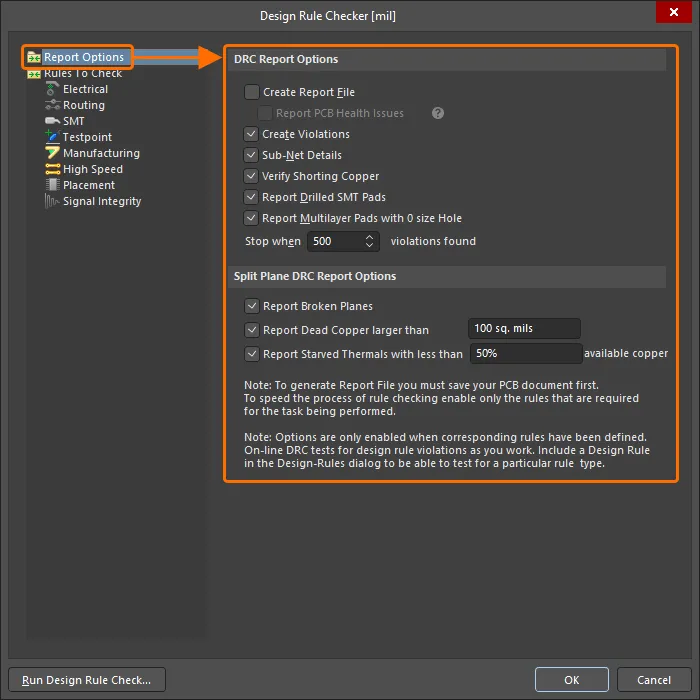
Настройка проверки правил проектирования выполняется в диалоговом окне Design Rule Checker, которое открывается с помощью команды Tools » Design Rule Check в главном меню.
-
Щелкните элемент Report Options в дереве слева в диалоговом окне, чтобы настроить дополнительные параметры, доступные при запуске Batch DRC.
-
Щелкните запись Rules to Check или запись для конкретной категории правил, чтобы загрузить диалоговое окно со списком типов правил и при необходимости включить каждый тип правила для Online и/или Batch DRC:
-
Online DRC – проверка будет выполняться в реальном времени по мере проектирования.
-
Batch DRC – проверка будет выполняться как пакетный процесс при нажатии кнопки Run Design Rule Check в диалоговом окне; результаты будут перечислены на панели Messages и, при необходимости, в сформированном отчете.
-


При запуске Online или Batch DRC обнаруженные нарушения правил будут обозначаться в рабочем пространстве проекта (с помощью пользовательской графики нарушений и/или наложения нарушений). Ниже показано несколько примеров нарушений в рабочем пространстве проекта:

Трассы, нарушающие правило Width. Нарушение обозначено как пользовательской графикой нарушений, так и наложением нарушений.

Трасса, нарушающая правило Net Antennae. Нарушение обозначено пользовательской графикой нарушений.
Вы можете настроить способ отображения нарушений различных типов правил в рабочем пространстве проекта на странице PCB Editor – DRC Violations Display диалогового окна Preferences.
На основе информации о степени отклонения от правила вы можете решить, как лучше устранить нарушение. Например, если ограничение для минимальной перемычки паяльной маски установлено на 0,25 мм, а фактическая перемычка составляет 0,24 мм, то ситуация не так уж плоха, и, возможно, вы сможете скорректировать ограничение, чтобы принять это значение. Но если фактическое значение перемычки равно 0,02, то, вероятно, такую ситуацию нельзя будет решить корректировкой ограничения.
-
Подробности приводятся на панели Messages. Фактическое значение указывается вместе с заданным значением (например, 0.017mm < 0.254mm).
-
Вы также можете щелкнуть правой кнопкой мыши по нарушению и открыть подменю Violations, чтобы посмотреть, какое ограничение нарушено и при каких условиях возникло нарушение (
 ).
).
-
PCB editor также включает удобные инструменты измерения, которые позволяют измерять расстояние между двумя точками, измерять выбранные объекты (длину выбранных трасс и дуг), а также расстояние между двумя примитивами. Подробнее см. на странице Измерение расстояний на PCB.
Панель PCB Rules And Violations — отличное средство для поиска и анализа условий нарушений. По умолчанию в списке Rule Classes будет показан элемент [All Rules]. Как только вы определите интересующий тип правила, выберите соответствующий класс правил, чтобы в нижней части панели отображались только эти нарушения. На панели приводятся тип нарушения, измеренное значение, ограничение и объекты, для которых зафиксировано нарушение. Обнаруженные нарушения правил для выбранного класса правил или конкретного правила также перечисляются в области Violations панели. Щелкните запись нарушения, чтобы выделить его в рабочем пространстве проекта в соответствии с настройкой в верхней части панели: Mask/Dim/Normal, Select, Zoom. Дважды щелкните по нарушению, чтобы открыть диалоговое окно Violation Details.

DRC также можно запускать для всех правил, правил определенного типа или конкретного правила, щелкнув правой кнопкой мыши соответствующую запись на панели PCB Rules And Violations и выбрав команду Run DRC.

Запускайте DRC прямо с панели PCB Rules And Violations. Здесь показан запуск DRC для всех определенных правил Clearance.
Подробнее о DRC: Design Rule Check (DRC).
 Локализовано с помощью ИИ