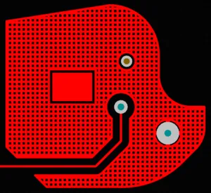
, используемая для создания большой области GND на плате")
Полигональная заливка (более яркий красный цвет), используемая для создания большой области GND на плате

Полигональная заливка показана как сплошной и штрихованной, демонстрируя различные зазоры и управляемый стиль подключения и воздушный зазор.
Полигональная заливка — это составной объект проектирования и состоит из более простых примитивов: либо регионов, либо дорожек и дуг. Полигональные заливки используются для создания сплошной или штрихованной (решётчатой) области на слое PCB, с использованием либо объектов-регионов либо комбинации объектов дорожек и дуг. Также называемые медными заливками, полигональные заливки похожи на регион за исключением того, что они могут заполнять области платы неправильной формы, поскольку автоматически «обтекают» существующие объекты, подключаясь только к объектам той же цепи (net), что и сама полигональная заливка.
На сигнальном слое можно разместить сплошную полигональную заливку, чтобы определить область для протекания больших токов питания, либо как область, подключённую к земле, для обеспечения электромагнитного экранирования. Штрихованные полигональные заливки обычно используются для земли в аналоговых проектах.
Полигональная заливка, размещённая на сигнальном слое, создаёт многоугольную (многогранную) область меди, которая может быть как сплошной, так и штрихованной. При заливке полигоны автоматически обеспечивают зазоры вокруг электрических объектов, принадлежащих другой цепи, подключаются к объектам той же цепи и заполняют области неправильной формы. Зазоры и свойства подключения управляются соответствующими правилами проектирования Electrical Clearance и Polygon Connection Style.
Полигональные заливки можно использовать и на немедных слоях. Если полигональная заливка размещена на несигнальном слое, она не будет «обтекать» существующие объекты, поскольку им не назначена цепь (net).
Размещение полигональной заливки
Полигональные заливки можно размещать только в PCB-редакторе. Чтобы разместить полигональную заливку напрямую, сначала переключитесь на нужный слой. После запуска команды размещения полигональной заливки (Place » Polygon Pour), курсор изменится на перекрестие, и вы перейдёте в режим размещения полигональной заливки. Установите курсор, затем щёлкните или нажмите Enter для размещения. Продолжайте размещать следующие полигональные заливки или щёлкните правой кнопкой мыши либо нажмите Esc для выхода из режима размещения.
-
В PCB-редакторе Altium Designer процесс определения любого многоугольного объекта — например, сплошного региона, контура платы или полигональной заливки — одинаков. Сплошные объекты являются замкнутыми, поэтому независимо от того, на каком этапе размещения вы находитесь, Altium Designer будет показывать линию от курсора обратно к начальной точке объекта. Эта линия станет последним ребром сплошного объекта, если вы щёлкнете правой кнопкой мыши (или нажмёте Esc) для выхода из режима размещения. Процесс размещения — это процесс задания контура многоугольного объекта, или, другими словами, задания положений углов с использованием различных доступных режимов углов.
-
Нажмите клавишу Tab во время размещения, чтобы приостановить размещение и открыть Properties панель в которой можно на лету изменить свойства размещаемой полигональной заливки, включая параметры заливки и подключения к цепи, а также свойства «обтекания» (pour-around). Нажмите кнопку паузы в оверлее (
 ), чтобы продолжить размещение. После завершения контура полигон автоматически зальётся в соответствии с параметрами, выбранными в Properties панели. Дополнительные сведения см. в разделе Polygon Pour Properties.
-
Полигональные заливки также можно создавать из выбранных примитивов. Существующий полигон можно разрезать на два или более полигонов, два или более объектов полигональной заливки можно объединить, а один или несколько объектов полигональной заливки можно вычесть из другого «базового» полигона. Подробнее см. в соответствующих разделах.
Режимы углов
При размещении полигональной заливки доступны пять режимов углов (45°, дуга 45°, 90°, дуга 90° и произвольный угол), причём у четырёх из них также есть подрежимы направления угла. Во время размещения:
-
Нажмите Shift+Spacebar, чтобы циклически переключаться между доступными режимами углов.
-
Нажмите Spacebar, чтобы переключаться между двумя подрежимами направления угла (кроме режима произвольного угла).
-
В любом из режимов дуговых углов удерживайте клавишу , или . чтобы уменьшать или увеличивать дугу. Удерживайте клавишу Shift при нажатии, чтобы ускорить изменение размера дуги.
-
Нажмите Backspace, чтобы удалить последний угол.
-
Нажмите сочетание клавиш 1, чтобы переключаться между размещением двух рёбер за один щелчок или одного ребра за один щелчок. Во втором режиме пунктирное ребро называется сегментом предварительного просмотра (look-ahead segment) (как показано на последнем изображении в наборе ниже; подробнее см. раздел Understanding the Look-Ahead Feature).


Нажмите Shift+Spacebar, чтобы циклически переключаться между пятью доступными режимами углов; нажмите сочетание 1, чтобы переключить размещение между двумя рёбрами или одним ребром.
Понимание функции Look-Ahead
Во многих ситуациях при проектировании PCB необходимо уметь предсказать, куда должен пойти будущий сегмент дорожки или ребро объекта, не фиксируя размещение этого объекта. Для поддержки этого требования в Altium Designer предусмотрена функция Look-Ahead. Когда Look-Ahead включён, ребро дорожки/объекта, которое в данный момент «прикреплено» к курсору, не размещается при щелчке; размещается только предыдущий сегмент. Иными словами, последний сегмент позволяет вам заглянуть вперёд — увидеть, где будет размещён следующий сегмент.
Нажмите сочетание клавиш 1 во время размещения объекта, чтобы включить или выключить Look-Ahead. Обратите внимание, как меняется отображение для каждого режима. При размещении дорожек сегменты, которые будут размещены следующим щелчком, показываются штриховкой, а сегмент Look-Ahead отображается как полый/пустой. При размещении сплошных объектов рёбра, которые будут размещены следующим щелчком, показываются сплошными белыми линиями, а ребро Look-Ahead — пунктирной белой линией.
Следующие изображения показывают, как меняется отображение сегмента дорожки при включённой и выключенной функции Look-Ahead.
 и выключенным (второе изображение). Следующий щелчок мышью разместит штрихованные сегменты дорожки.") Размещение дорожки с включённым Look-Ahead (первое изображение) и выключенным (второе изображение). Следующий щелчок мышью разместит штрихованные сегменты дорожки.
Размещение дорожки с включённым Look-Ahead (первое изображение) и выключенным (второе изображение). Следующий щелчок мышью разместит штрихованные сегменты дорожки.
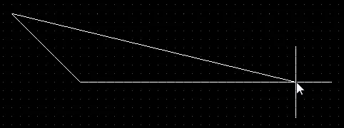
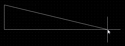
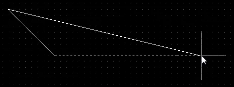
Функция Look-Ahead также работает при размещении полигональной заливки. Нажмите 1 во время размещения чтобы включить или выключить её (обратите внимание, что это сочетание работает только во время размещения объекта). Следующие изображения показывают размещение первого угла полигональной заливки.
 Look-Ahead включён. При следующем щелчке мышью сплошная линия станет ребром полигона, а пунктирная — нет. Обратите внимание на сплошную линию возврата: она показывает, как полигон будет замкнут, если вы завершите размещение полигона.
 Look-Ahead выключён. При следующем щелчке обе сплошные линии станут рёбрами полигона. Обратите внимание на сплошную линию возврата: она показывает, как полигон будет замкнут, если вы завершите размещение полигона.
Редактирование полигона
Перемещение полигональной заливки
Щёлкните по самой форме выбранной полигональной заливки (в стороне от её маркеров редактирования) и перетащите, чтобы переместить её. Удерживайте клавишу Shift, чтобы выбрать несколько полигональных заливок для перемещения.
Дополнительные действия, которые можно выполнять во время перемещения:
-
Нажмите Spacebar, чтобы повернуть полигональную заливку против часовой стрелки, или Shift+Spacebar — по часовой стрелке. Поворот выполняется в соответствии со значением Rotation Step заданным на странице PCB Editor – General page диалога Preferences.
-
Нажмите клавишу L, чтобы перевернуть полигон на другую сторону платы.
-
Нажмите клавиши X или Y, чтобы отзеркалить полигон относительно оси X или оси Y соответственно.
Либо можно щёлкнуть правой кнопкой мыши по полигональной заливке и выбрать в контекстном меню команду Polygon Actions » Move Polygon . После запуска команды полигональная заливка «прикрепится» к курсору и будет отображаться в контурном режиме. Переместите полигональную заливку в нужное положение, затем щёлкните или нажмите Enter для размещения.
Изменение формы полигональной заливки
 Полигональная заливка с дуговыми углами 90º, размер которой изменяется.
Выбранная полигональная заливка содержит два типа точек или «маркеров», с помощью которых редактируется её форма.
-
Full Handles - эти заполненные маркеры расположены в углах полигона.
-
Empty Handles - эти пустые маркеры расположены в центрах сегментов, созданных Full Handles.
Существующий полигон можно изменить, перемещая эти маркеры (вершины), расположенные в каждом углу или в центре каждого ребра.
Чтобы изменить форму полигона:
-
Щёлкните и выберите полигон — вершины полигона подсветятся, а курсор изменится на перекрестие.
-
Щёлкните, удерживайте и перетащите Full Handle, чтобы переместить соответствующий угол.
-
Щёлкните, удерживайте и перетащите вдоль ребра, чтобы переместить всё ребро целиком.
-
Щёлкните, удерживайте и перетащите Empty Handle, чтобы переместить всю сторону (для дорожки и для дуги).
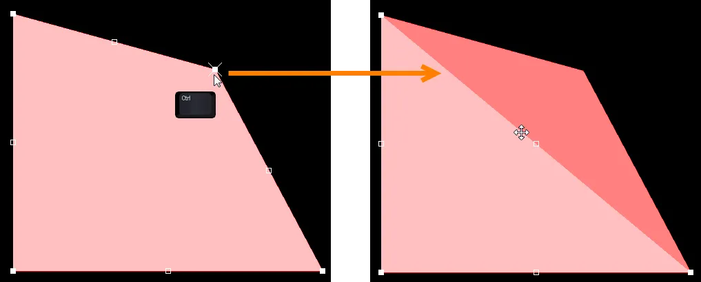
-
Ctrl+Click щёлкните по Empty Handle, чтобы разделить это ребро на два ребра. Ctrlнужно удерживать только в начале перемещения. Затем можно использовать горячие клавиши Shift+Spacebar, чтобы циклически переключаться между режимами (дуга, фаска и произвольный угол).

На верхних изображениях показано редактирование пустой ручки. На нижних изображениях Ctrl был нажат при захвате ручки для перемещения с целью редактирования.
-
Если режим размещения «произвольный угол» создает нежелательные вершины, щелкните и удерживайте вершину, затем перетащите ребро, чтобы уменьшить количество вершин на этом ребре до одной. Чтобы удалить вершину, щелкните и удерживайте вершину так, как будто собираетесь ее переместить, затем нажмите клавишу Delete .
-
Когда закончите, щелкните правой кнопкой мыши и выберите Polygon Actions » Repour Selected, чтобы заново залить полигон в его новой форме.
Изменение границы заливки полигона
Помимо редактирования вершин, вы также можете использовать команду контекстного меню Polygon Actions » Modify Polygon Border, чтобы легко изменить форму полигонов. После запуска команды курсор принимает вид перекрестия. Каждый раз при щелчке добавляется новая вершина. Как и при размещении полигона, сочетания клавиш Shift+Spacebar можно использовать для изменения формы углов.
Изменение размера заливки полигона
Чтобы переключиться с редактирования формы на редактирование размера выбранного объекта заливки полигона, находящегося под курсором, можно щелкнуть правой кнопкой мыши по выбранному объекту заливки полигона и затем выбрать в контекстном меню команду Polygon Actions » Resize Polygon . После запуска команды режим редактирования полигона изменится с reshaping на resizing. Это визуально подтверждается тем, что ручки редактирования вдоль каждой кромки полигональной формы заменяются восемью ручками редактирования, расположенными по углам (и в центрах) ограничивающего прямоугольника объекта.
-
Щелкните и перетащите угловую ручку редактирования, чтобы изменить размер заливки полигона одновременно по вертикали и по горизонтали.
-
Щелкните и перетащите центральную ручку редактирования, чтобы изменить размер заливки полигона отдельно по вертикали или по горизонтали.
По мере изменения размера заливки полигона контур его прежней формы сохраняется до тех пор, пока измененный полигон не будет заново залит, — это служит указанием на изменение.
После изменения размера или положения заливки полигона она будет помечена как измененная. Если параметр Repour Polygons After Modification включен на странице PCB Editor - General диалога Preferences , полигон (и все зависящие от него объекты) будет автоматически перезалит. Если этот параметр не включен, заливка полигона не будет перезалита.
Чтобы переключиться с редактирования размера обратно на редактирование формы, щелкните правой кнопкой мыши по выбранному объекту заливки полигона, размер которого сейчас изменяется, и выберите в контекстном меню команду Polygon Actions » Edit Polygon Shape .
Свойства заливки полигона

Режим Polygon Pour панели Properties
| Actions |
-
Repour — нажмите, чтобы перезалить полигон. Эта функция полезна, если вы изменили проект внутри полигона. После восстановления его нужно перезалить, чтобы устранить любые нарушения, возникшие из‑за изменений в проекте.
-
Shelve — нажмите, чтобы «убрать на полку» (shelve) полигон: он не удаляется из проекта, но скрывается из отображения, а также исключается из DRC и анализа связности цепей.
-
Assign net — нажмите, чтобы назначить цепь (net) выбранному полигону. После выбора появится диалог Net Name.
-
Bring to front — нажмите, чтобы изменить порядок заливки так, чтобы выбранный полигон оказался перед всеми другими перекрывающимися полигонами (имел наивысший приоритет).
-
Send to back — нажмите, чтобы изменить порядок заливки так, чтобы выбранный полигон оказался позади всех других перекрывающихся полигонов (имел наименьший приоритет).
-
Modify — нажмите, чтобы переопределить форму полигона непосредственно в документе PCB.
|
| Net Information |
Информация о цепи, к которой относится заливка полигона, а также о дифференциальной паре, если эта цепь является ее участником. При необходимости также отображается информация о классе. См. страницу PCB Placement & Editing Techniques , чтобы узнать больше об информации по цепям. |
| Net |
Цепь, участником которой является эта заливка полигона. Все цепи активного проекта платы будут перечислены в раскрывающемся списке. Выберите No Net , чтобы указать, что полигон не подключен ни к одной цепи. Свойство примитива Net используется проверкой правил (Design Rule Checker) для определения, корректно ли размещен объект PCB. Кроме того, можно щелкнуть значок Assign Net ( ), чтобы выбрать объект в рабочем пространстве — цепь этого объекта будет назначена выбранному полигону(ам). См. страницу PCB Placement & Editing Techniques , чтобы узнать больше о назначении цепей объектам. ), чтобы выбрать объект в рабочем пространстве — цепь этого объекта будет назначена выбранному полигону(ам). См. страницу PCB Placement & Editing Techniques , чтобы узнать больше о назначении цепей объектам. |
| Layer |
Используйте раскрывающийся список, чтобы выбрать слой, на котором размещена заливка полигона. |
| Name |
Задайте подходящее имя для полигона. Помимо упрощения идентификации каждого полигона, имя можно использовать для нацеливания на конкретный полигон (или семейство полигонов) в правиле проектирования. По умолчанию к полигону применяется автоматическое именование на основе слоя и цепи. Именование выполняется по выбранной схеме именования, указанной в поле Polygon Naming Scheme режима Board панели Properties. Если вы ввели пользовательское имя и хотите вернуться к автоматическому именованию, просто очистите поле и нажмите Enter.
-
Сброс пользовательского имени и возврат к автоматическому именованию также можно выполнить из панели PCB List и Polygon Pour Manager.
-
Автоматически назначенные имена постоянно отслеживаются и управляются в Altium Designer. Если изменяется атрибут, например назначение цепи или положение слоя в стеке слоев, автоматически назначенное имя обновляется автоматически. Затронутые правила проектирования также обновляются автоматически.
|
| Area |
Площадь, которую охватывает данная заливка полигона, в квадратных миллиметрах или квадратных дюймах. |
| (X/Y) |
Текущее положение первой вершины этой заливки полигона в рабочем пространстве относительно задаваемого пользователем начала координат. Нажмите кнопку  , чтобы зафиксировать положение этой заливки полигона. См. страницу PCB Placement & Editing Techniques , чтобы узнать больше о фиксации объектов проекта. , чтобы зафиксировать положение этой заливки полигона. См. страницу PCB Placement & Editing Techniques , чтобы узнать больше о фиксации объектов проекта. |
| Fill Mode |
Выберите режим заполнения для заливки полигона. Доступны три режима, каждый со своими преимуществами и параметрами. Подробнее см. Polygon Pour Fill Modes. |
| Pour Over Same Net |
Используйте раскрывающийся список, чтобы управлять поведением заливки при встрече объектов той же цепи. Подробнее см. Connecting the Polygon Pour to a Net. |
| Remove Dead Copper |
При заливке полигона могут образовываться области (островки) полигона, полностью изолированные от подключенной цепи из‑за наличия других дорожек, площадок и т. п. Если этот параметр включен, любая область полигона, в которой нет хотя бы одного соединения с другим объектом цепи, автоматически удаляется. Обратите внимание: если ваш полигон не охватывает ни одной площадки назначенной цепи, то это полностью «мертвая» медь, и она будет удалена целиком. В этой ситуации контур полигона все равно отображается, чтобы показать, что в этом месте существует полигон.
|
| Optimal Void Rotation |
Включите этот параметр, чтобы обеспечить такое построение кромок полигона, при котором достигается максимальная ширина «шейки» там, где полигон проходит между соседними объектами, принадлежащими другим цепям. Дуги полигона заменяются короткими прямыми сегментами, длины которых определяются настройкой Arc Approx..
|
| Outline Vertices |
Используйте эту область для изменения отдельных вершин выбранного в данный момент объекта polygon pour. Вы можете изменять положение существующих вершин, добавлять новые вершины или удалять их при необходимости. Можно задавать дуговые соединения между точками вершин; также предусмотрена поддержка экспорта информации о вершинах в и импорта из файла в формате CSV.
-
Vertices Grid – перечисляет все точки вершин, определённые в данный момент для polygon pour.
-
Index – назначенный индекс вершины (не редактируется).
-
X – координата X (горизонтальная) для вершины. Щёлкните, чтобы отредактировать.
-
Y – координата Y (вертикальная) для вершины. Щёлкните, чтобы отредактировать.
-
Arc Angle (Neg=CW) – угол дуги, которая рисуется для соединения этой точки вершины со следующей. По умолчанию соединения представляют собой прямолинейные рёбра, и это поле остаётся пустым. Щёлкните, чтобы отредактировать, затем при необходимости введите угол дуги. Ввод положительного значения приведёт к построению дуги против часовой стрелки. Чтобы построить дугу по часовой стрелке, введите отрицательное значение.
-
Add – используется для добавления новой точки вершины. Новая вершина будет добавлена ниже текущей выбранной (подсвеченной) записи вершины и изначально будет иметь те же координаты, что и ранее выбранная запись.
-
 – щёлкните, чтобы удалить текущую выбранную запись вершины. Перед удалением будет запрошено подтверждение. – щёлкните, чтобы удалить текущую выбранную запись вершины. Перед удалением будет запрошено подтверждение.
Чтобы экспортировать всё содержимое таблицы в файл в формате CSV, щёлкните правой кнопкой мыши в любом месте таблицы и выберите команду Export To CSV. Появится диалог Export Outline Vertices, в котором можно указать, где и под каким именем будет сохранён файл. По умолчанию файл будет называться Outline Vertices.CSV. Чтобы импортировать информацию о вершинах из CSV-файла, щёлкните правой кнопкой мыши в любом месте таблицы и выберите команду Import From CSV. Появится диалог Import Outline Vertices, с помощью которого можно найти и открыть нужный CSV-файл. Обратите внимание: импорт перезапишет всё, что в данный момент определено в таблице.
|
Если были внесены какие-либо изменения — вручную или путем импорта данных из CSV-файла — панель отметит, что изменения ожидают применения, синим баннером в верхней части панели Properties и предложит применить их.
Режимы заливки полигона
, затем залитый с использованием дорожек/дуг (Hatched).")
Один и тот же полигон, залитый с использованием регионов (Solid), затем залитый с использованием дорожек/дуг (Hatched).
Движок размещения заливки полигона может строить полигоны либо из сплошных регионов, либо из комбинации дорожек и дуг — в зависимости от режима заливки, выбранного в панели Properties. Изображение предварительного просмотра меняется, показывая графическое представление сплошной заливки полигона, и в панели предоставляются связанные параметры. Поддерживаются три режима заливки.
Каждый параметр режима заливки отображает опцию Show Preview / Hide Preview в панели Properties. Используйте ее, чтобы показать или скрыть визуальное представление выбранного полигона в панели.
Сплошной
При выборе этого режима полигон внутренне строится из объектов сплошных регионов, при этом для каждой непрерывной области меди в завершенном полигоне создается отдельный регион.
Полигон этого типа выводится в Gerber с использованием определений Gerber-регионов. Обратите внимание: круговые вырезы не поддерживаются в определении Gerber-региона, поэтому дуги (отверстия) для круговых вырезов фактически аппроксимируются прямыми хордовыми сегментами. Их точность задается параметром Arc Approx. в панели Properties. Полигоны этого типа приводят к размещению значительно меньшего числа объектов, что дает: меньшие файлы; более быструю заливку и перерисовку, открытие файла, DRC и анализ связности цепей; а также меньшие выходные файлы, поскольку объект региона полностью поддерживается в Gerber и ODB++.
При выборе этого режима в панели Properties доступны следующие связанные параметры ( ).
).
| Remove Islands Less Than |
Задайте значение площади. Любые области меди, площадь которых меньше этого значения, будут удалены.
Эта опция основана только на площади; она не учитывает, подключен ли этот «островок» к площадке или переходному отверстию. Обратите внимание: все неподключенные области меди всегда удаляются, если в панели Properties включена опция Remove Dead Copper.
|
| Arc Approx. |
Задайте максимальное отклонение от идеальной дуги (криволинейные кромки создаются из множества коротких прямых сегментов). Уменьшение этого значения приведет к использованию большего числа прямых сегментов для более точной аппроксимации дуги. |
| Remove Necks Less Than |
Задайте значение ширины. Узкие «слivers» меди, ширина которых меньше этого значения, будут удалены. Обратите внимание: при большем значении этой опции будет больше тесных мест, где полигон не сможет залиться. Обычно это значение задают не меньше минимальной ширины дорожки, используемой в проекте, или минимальной ширины меди, поддерживаемой производителем. Включите опцию Obey Rules чтобы взять значение из соответствующего минимального ограничения Width. |
Штриховой
При выборе этого режима полигон создается из объектов дорожек и дуг. Контур штрихового полигона формируется из дорожек и дуг, при этом заданная пользователем граница полигона проходит по центральной линии контурных дорожек и дуг.
Полигоны этого типа обычно заливаются медленнее и приводят к увеличению размеров файлов PCB и Gerber. Штриховые полигоны часто используются в аналоговых проектах.
При выборе этого режима в панели Properties доступны следующие связанные параметры ( ).
).
| Track Width |
Задайте ширину дорожки, используемой для создания полигона. |
| Grid Size |
Задайте шаг (интервал) или сетку, по которой размещаются дорожки для штрихованного полигона.
Регулируя параметры Track Width и Grid Size объектов дорожка/дуга, можно получить завершённый полигон либо штрихованным (если Track Width меньше Grid Size), либо сплошным (если Track Width равно или больше Grid Size) по виду.
|
| Surround Pad With |
Укажите форму, используемую для обрамления площадок: Arcs или Octagons. |
| Hatch mode |
Доступны четыре режима: 90 Degree, 45 Degree, Horizontal или Vertical. |
| Min Prim Length |
Укажите, насколько короткими допускается делать объекты дорожка/дуга в режиме заливки. |
| Obey Polygon Cutout |
Включите эту опцию, если штрихованная заливка полигона не должна заходить за границы выреза заливки полигона. Когда эта опция отключена, осевые линии дорожек заливки полигона будут располагаться вдоль границ выреза заливки полигона. |
Нет
Этот режим по сути такой же, как режим Hatched . Он также использует дорожки и дуги для задания границ, но заполняющие дорожки и дуги не добавляются.
Этот режим может быть полезен при анализе структуры и конструкции различных полигонов и попытках понять взаимодействие перекрывающихся полигонов. Он также полезен, когда вносятся изменения в проект, а полигон мешает процессу. Альтернативный подход к использованию контуров при внесении изменений — отложить полигоны, при этом они сохраняются в файле PCB но убираются из вида.
Следующие связанные параметры доступны на панели Properties, когда выбран этот режим ( ).
).
| Track Width |
Укажите ширину дорожки для контура заливки полигона. |
| Surround Pad With |
Укажите формы для обрамления площадок: Arcs или Octagons. |
| Min Prim Length |
Укажите, насколько короткими допускается делать объекты дорожка/дуга в режиме заливки. |
| Obey Polygon Cutout |
Включите эту опцию, если контурная заливка полигона не должна заходить за границы выреза заливки полигона. Когда эта опция отключена, осевые линии дорожек заливки полигона будут располагаться вдоль границ выреза заливки полигона. |
Подключение заливки полигона к цепи
Полигон можно привязать к цепи. Выберите нужную цепь в раскрывающемся списке Net на панели Properties . Заливка полигона подключится к каждой площадке и переходному отверстию этой цепи, которые находятся внутри контура полигона, в соответствии с применимым правилом проектирования Polygon Connect Style. Обратите внимание: при необходимости правило поддерживает задание разных способов подключения для выводных (thru-hole) площадок, SMD-площадок и переходных отверстий. Зазор между полигоном и объектами, принадлежащими другим цепям, определяется применимым правилом проектирования Electrical Clearance.
То, как заливка полигона обрабатывает другие объекты в той же цепи, включая трассировочные дорожки, дуги, заливки и регионы, определяется параметром, выбранным в раскрывающемся списке Pour Over Same Net на панели Properties при выделенной заливке полигона:
-
Don't Pour Over Same Net Objects – выберите этот вариант, если вы специально not хотите, чтобы полигон заливался поверх объектов дорожка, дуга, заливка, регион или полигон в этой (или любой другой) цепи, т.е. чтобы полигон заливался только в свободном пространстве.
-
Pour Over All Same Net Objects – выберите этот вариант, если вы хотите, чтобы полигон заливался в свободном пространстве, а также поверх all объектов (т.е. дорожек, дуг, заливок, регионов, других полигонов) в той же цепи, что и полигон, находящихся в области полигона. Например, существующая трассировка этой цепи будет полностью перекрыта полигоном.
-
Pour Over Same Net Polygons Only – выберите этот вариант (по умолчанию), если вы хотите, чтобы полигон заливался только в свободном пространстве и поверх существующих объектов заливки полигона внутри его границы, которые принадлежат той же цепи. Полигон будет обходить все остальные объекты (дорожки, дуги, заливки и регионы) независимо от того, к какой цепи они принадлежат.
Если заливка полигона размещена на несигнальном слое, она не будет обходить существующие объекты, поскольку эти объекты не назначены цепи и, следовательно, ни к чему не относятся.
Скрытие (Shelving) и восстановление (Restoring) заливки полигона
В процессе проектирования нормально, что происходят изменения — компоненты могут добавляться или изменяться, трассировку может потребоваться обновить и т. д. Чтобы упростить управление существующими полигонами в ходе этого процесса, их можно shelved. Это временно скрывает их из отображения, а также из движков DRC и анализа связности цепей, но сохраняет их в базе данных PCB (т. е. они не уничтожаются и могут быть восстановлены в любое время). Это позволяет вносить изменения в компоновку платы как с визуальным удобством, так и без влияния на производительность — как редактирования, так и DRC — которое могут создавать визуальные заливки полигонов.
-
Чтобы скрыть все заливки полигонов в текущем проекте, выберите Tools » Polygon Pours » Shelve <n> Polygon(s) в главном меню (где <n> — количество заливок полигонов, обнаруженных в проекте).
-
Чтобы восстановить все скрытые заливки полигонов, выберите команду Tools » Polygon Pours » Restore <n> Shelved Polygon(s) в главном меню (где <n> — количество заливок полигонов, которые сейчас скрыты). Все восстановленные полигоны рассматриваются так, как будто они были изменены. Если опция Repour Polygons After Modification включена на странице PCB Editor - General диалога Preferences, заливки полигонов и все их зависимые объекты будут автоматически перезалиты (repour). Если эта опция отключена, восстановленные заливки полигонов не будут перезалиты.
-
Также можно выборочно скрывать полигоны через команды подменю Polygon Actions по правому клику или в диалоге Polygon Pour Manager.
Перезаливка (Repouring) полигона
Если вы изменили проект внутри полигона, после его восстановления потребуется выполнить перезаливку, чтобы устранить любые нарушения, возникшие из‑за изменений. Существует несколько способов перезалить (перестроить) полигон в текущем документе.
Чтобы перезалить полигон, щёлкните по полигону правой кнопкой мыши, затем выберите команду Repour из подменю Polygon Actions или используйте соответствующую команду Repour в подменю Tools » Polygon Pours :
-
Repour Selected - перезалить все выбранные заливки полигонов (и их зависимые объекты).
-
Repour All - перезалить все определённые (и не скрытые) заливки полигонов.
-
Repour Violating Polygons - перезалить все заливки полигонов с нарушениями.
-
Repour Modified - перезалить все изменённые заливки полигонов. Изменённая заливка полигона — это та, которая была каким‑то образом изменена, но ещё не была перезалита. Её свойство IsModified — которое можно увидеть в панели PCB List panel для выбранной заливки полигона — включено (True).
Заливки полигонов также можно перезаливать в диалоге Polygon Pour Manager (Tools » Polygon Pours » Polygon Manager), выбрав нужный полигон и нажав кнопку Repour.
Подтвердите изменения в диалоге Confirm.
Чтобы редактировать полигон, слой, на котором находится полигон, должен быть текущим или активным слоем.
Если опции Repour Polygons After Modification и Repour all dependent polygons after editing включены на странице PCB Editor - General page диалога Preferences, заливка полигона и все её зависимые объекты будут автоматически перезалиты после изменения.
Настройка порядка заливки
Когда два полигона перекрываются, Altium Designer нужно знать, какой из них должен занять общую область перекрытия. Это выполняется путем задания порядка заливки (pour order): полигон с более высоким порядком имеет приоритет и заливает общую область. Порядок заливки перекрывающихся полигонов можно настроить интерактивно — щелкните правой кнопкой мыши по выбранной заливке полигона и выберите одну из следующих команд в контекстном меню:
-
Polygon Actions » Bring to front - изменить порядок заливки так, чтобы выбранный полигон оказался перед всеми остальными перекрывающимися полигонами (и, следовательно, имел наивысший приоритет).
-
Polygon Actions » Send to back - изменить порядок заливки так, чтобы выбранный полигон оказался позади всех остальных перекрывающихся полигонов (и, следовательно, имел наименьший приоритет).
Измененный порядок будет визуально отображен в рабочей области после повторной заливки полигона, который теперь считается измененным.
Управление стилем подключения полигона
Main page: Правило проектирования Polygon Connect Style
То, как полигон подключается к площадкам цепи, к которой он привязан, определяется соответствующим Plane » Polygon Connect Style правилом проектирования (Design » Rules).

То, как полигон подключается к площадкам цепи, определяется Polygon Connect Style правилом проектирования.
Доступны три варианта подключения:
-
Relief Connect - создается подключение «спицами». Задайте Number проводников, Angle этих проводников (90º или 45º), Conductor Width и Air Gap Width (зазор между краем площадки и краем полигона, окружающего площадку).
-
Direct Connect - полигон фактически заливает площадку — создается сплошная медь к выводу.
-
No Connect - площадки данной цепи будут изолированы от полигона.
Параметр Air Gap Width управляет зазором между краем площадки и окружающим полигоном, тогда как в более ранних версиях Altium Designer это делали правила проектирования Electrical Clearance. При открытии платы, разработанной в более ранней версии Altium Designer, появится предупреждение. В этой ситуации важно проверить и задать параметры Air Gap Width в правилах проектирования Polygon Connect Style.
Управление зазором полигона
Main page: Правило проектирования ClearanceКак и для любого объекта, размещенного на сигнальном (медном) слое, зазор полигона относительно объектов, вокруг которых он заливается, определяется соответствующим Electrical Clearance правилом проектирования.
 Зазор от полигона до объектов других цепей определяется правилом проектирования Electrical Clearance.
Обычно практикуется увеличенный зазор между полигоном и объектами других цепей. Чтобы этого добиться, можно определить отдельное, «полигон-специфичное» правило проектирования Electrical Clearance. Пример показан на изображении выше. Помните, что правило Polygon Clearance также должно иметь более высокий Priority , чем любое общее правило зазоров, иначе оно не будет влиять на результат.
При определении правила Electrical Clearance для полигонов необходимо использовать ключевое слово запроса InPolygon (или InPoly) вместо IsPolygon (или IsPoly). Это связано с тем, что правила зазоров работают с примитивами (областями, дорожками и дугами), из которых состоит полигон или которые in его формируют, а не с полигоном как с единым объектом. Корректное правило зазора для заливок полигонов может быть задано между объектами InPolygon и All другими объектами.
Вырезы в заливке полигона
Вырез в заливке полигона по сути является отрицательной медной областью — вы задаете пустоту или отверстие в полигоне. Чтобы определить вырез в полигоне:
-
Выберите команду Place » Polygon Pour Cutout в главном меню.
-
Курсор изменится на перекрестие, начиная внутри границы полигона. Щелкните, чтобы задать начальную точку.
-
Перемещайте курсор по полигону. Нажмите Shift+Spacebar, чтобы переключать режимы углов области.
-
Продолжайте щелкать и перемещать мышь, чтобы задать контур выреза.
-
Щелкните правой кнопкой мыши, чтобы выйти из режима размещения выреза.
-
Теперь исходный полигон нужно повторно залить. Щелкните по нему, чтобы выделить, затем используйте команду Tools » Polygon Pours » Repour Selected в главном меню — заливка выполнится с учетом нового выреза.
Вырез фактически является объектом Region object с включенной опцией Polygon Cutout. При необходимости его можно перемещать, изменять размер или удалять. Чтобы изменить размер выреза, щелкните по нему один раз для выделения, затем щелкните и удерживайте, чтобы перетащить ребро или вершину. Помните, что полигон необходимо повторно заливать каждый раз, когда вырез изменяется.
; полигон повторно залит (второе изображение).")
Вырез размещен (первое изображение); полигон повторно залит (второе изображение).
Создание заливки полигона из набора дорожек
Помимо задания областей электрической меди на плате, полигоны и сплошные области также используются для создания других объектов полигональной формы, например специального символа или логотипа компании. Если контур требуемой формы был определен в другом инструменте проектирования, например AutoCAD, его можно экспортировать в файл DXF, а затем импортировать в Altium Designer. После этого контур можно преобразовать в полигон или сплошную область.
Чтобы преобразовать замкнутую границу, составленную из выбранных объектов дорожек и/или дуг, в полигон, выделите все примитивы, формирующие замкнутую фигуру, затем выберите Tools » Convert » Create Polygon from Selected Primitives в главном меню.
Обратите внимание:
-
Полигон будет создан на текущем (активном) слое, а не на слое, на котором находятся выбранные дорожки. Это означает, что вы можете задать форму на механическом слое, а затем создать полигон на сигнальном слое.
-
Изначально выбранные примитивы не удаляются — они будут существовать и после создания полигона и останутся выделенными. Новый полигон заливается внутри выбранных объектов.
-
Граница нового полигона будет проходить по осевой линии выбранных объектов, использованных для его создания.
-
Если полигон создается на том же слое, что и выбранные дорожки, он будет заливаться внутри дорожек в соответствии с применимым правилом проектирования Electrical Clearance.
-
Полигон будет создан с режимом заливки None. Дважды щелкните, чтобы повторно залить новый полигон как сплошной или штрихованный.
Поскольку алгоритм Create Polygon from Selected Objects использует осевую линию выбранных объектов, он требует, чтобы конечные и начальные точки соприкасающихся объектов точно совпадали (начинались/заканчивались в одной и той же точке X, Y). Если это не так, появится диалоговое окно Confirm, в котором будет указано место, где алгоритм не сработал, а также будет предложена возможность указать алгоритму попытаться определить полигон по краям объектов вместо осевых линий. Если выбранные объекты хотя бы немного перекрываются, этот вариант должен создать полигон, граница которого будет повторять внешний край выбранных объектов.
Разрезание заливки полигона
Одну заливку полигона можно разрезать на две или более отдельных заливок. Для этого:
-
Убедитесь, что текущим сделан правильный слой, поскольку инструмент разрезания работает только при условии, что текущий слой — это слой, на котором находится разрезаемая заливка полигона.
-
Выберите Place » Slice Polygon Pour в главном меню (или команду Slice Polygon Pour на Active Bar, либо команду Polygon Actions » Slice Polygon Pour в меню, вызываемом правой кнопкой мыши по заливке полигона).
-
После выбора команды вы переходите в режим разрезания (аналогично режиму размещения дорожек), и курсор изменится на перекрестие. Начиная снаружи границы полигона, щелкните, чтобы зафиксировать начальную точку линии разреза (первого сегмента дорожки).
- Перемещайте курсор по полигону. Процесс разрезания использует режим размещения линии (Line placement mode) для задания как траектории разреза, так и его ширины. При задании разреза:
-
Нажмите Shift+Spacebar, чтобы циклически переключать режимы углов при размещении линии.
-
Нажмите Spacebar для переключения между режимами угла Start и End.
-
Нажмите Backspace чтобы удалить последний установленный угол.
-
Нажмите Tab, чтобы открыть диалог Line Constraints и изменить ширину линии и/или текущий слой для размещения.

Диалог Line Constraints.
-
Line Width — используйте это поле, чтобы ввести новую ширину линии. Эта новая ширина будет применена к сегменту, который размещается в данный момент.
-
Current Layer — используйте это поле, чтобы переключить слой, на котором размещается линия. В раскрывающемся списке перечислены все слои платы, определённые в данный момент (и включённые). Выбранный слой будет применён к «опережающему» сегменту линии, то есть к сегменту после того, который размещается сейчас.
-
Щёлкните для фиксации серии вершин, определяющих линию разреза.
-
После того как линия разреза будет проложена через полигон и выйдет с другой стороны, щёлкните правой кнопкой мыши или нажмите Esc для завершения размещения линии.
-
Щёлкните правой кнопкой мыши второй раз, чтобы завершить разрезание. Появится диалог Confirm с вопросом, хотите ли вы разделить полигон; нажмите Yes, чтобы разделить его.
Поскольку теперь это два независимых полигона, каждый из них можно редактировать и перепроливать (repour) по мере необходимости.
Поскольку линия разреза имеет тот же цвет, что и заливка полигона, полезно перед началом процесса разрезания перепролить полигон с режимом заливки, установленным в None, чтобы линию разреза было хорошо видно.
Обратите внимание: разделённые секции полигона фактически не помечаются как изменённые, поэтому перепролив «изменённых полигонов» не даст эффекта. Чтобы зафиксировать разрез(ы) — и визуально увидеть их в рабочем пространстве — потребуется выполнить перепролив вручную: либо выбрав «части» полигона и используя команду Repour Selected либо используя команду Repour All.
Объединение выбранных заливок полигонов
Два или более объектов polygon pour можно объединить, выполнив следующую последовательность действий:
-
Разместите новые (или перетащите существующие polygon pours) так, чтобы они перекрывали друг друга нужным образом.
-
Выберите все polygon pours, которые нужно объединить.
-
Щёлкните правой кнопкой мыши по одной из заливок в выделении и затем выберите команду Polygon Actions » Combine Selected Polygons в контекстном меню.
Свойства нового полигона копируются из первого выбранного полигона в каждой группе пересекающихся объектов.
Вычитание выбранных заливок полигонов
Один или несколько объектов polygon pour можно вычесть из другого «базового» polygon pour выполнив следующую последовательность действий:
-
Разместите новые или перетащите существующие polygon pours так, чтобы они перекрывали требуемый базовый polygon pour — это заливка, из которой будет выполняться «вычитание».
-
Выберите базовый polygon pour, щёлкните правой кнопкой мыши и затем выберите команду Polygon Actions » Subtract Polygons From Selected в контекстном меню.
-
Выберите полигоны, которые нужно вычесть.
-
Щёлкните правой кнопкой мыши или нажмите Esc для завершения процесса.
Разбиение polygon pour на примитивы
Заливку polygon pour можно вернуть к различным примитивам, из которых она была создана, выбрав команду Tools » Convert » Explode Polygon to Free Primitives в главном меню или щёлкнув правой кнопкой мыши по размещённой заливке polygon pour (выделенной или нет) и затем выбрав команду Polygon Actions » Explode Polygon To Free Primitives (или Explode Selected Polygons To Free Primitives) в контекстном меню. Сплошные полигоны будут преобразованы обратно в примитивы region, а штрихованные — в дорожки и дуги. После разбиения объект polygon pour больше нельзя будет обрабатывать как групповой объект.
Хотя отдельной команды для повторной группировки «взорванного» полигона нет, вы можете использовать команду Undo, чтобы добиться этого.
Диалог Polygon Pour Manager
Диалог Polygon Pour Manager предоставляет обзор верхнего уровня всех полигонов, которые в данный момент существуют в рабочем пространстве PCB. Диалог также позволяет задавать/изменять имя каждого полигона, устанавливать порядок заливки полигонов, выполнять перепролив или «снятие на полку» (shelving) для выбранных полигонов, а также добавлять/задавать область действия (scope) правил проектирования для выбранных полигонов.
Чтобы открыть диалог Polygon Pour Manager выберите команду Tools » Polygon Pours » Polygon Manager в главном меню или щёлкните правой кнопкой мыши по размещённой заливке polygon pour в рабочем пространстве и затем выберите команду Polygon Actions » Polygon Manager в контекстном меню.

Диалог Polygon Pour Manager даёт вам полный контроль над всеми полигонами в проекте.
После запуска команды откроется диалог Polygon Pour Manager . Диалог можно использовать для всего неграфического редактирования polygon pours в проекте, включая элементы управления для:
-
Переименования полигонов (включая возможность использовать функцию Auto-Naming).
-
Задания порядка заливки полигонов.
-
Перепролива всех или отдельных полигонов (изменённых/выбранных/с нарушениями).
-
«Снятия на полку» (shelve) или возврата (unshelve) всех или выбранных полигонов.
-
Блокировки или разблокировки всех или выбранных полигонов.
-
Игнорирования или сохранения нарушений для всех или выбранных полигонов (в отношении Online DRC).
-
Добавления/задания области действия (scope) правил стиля подключения полигона и зазоров (clearance).
-
Добавления классов полигонов для выбранных полигонов.
-
Создания нового полигона на основе выбранного полигона или контура платы.
Options and Controls of the Polygon Pour Manager Dialog
Просмотр/Редактирование
Это список всех существующих полигонов в документе PCB. Список Pour Order группирует polygon pours по слоям, показывая только те заливки полигонов, которые находятся на том же слое, что и текущая выбранная заливка polygon pour (или первая выбранная, если выбрано несколько заливок на разных слоях). Щёлкните заголовок столбца, чтобы отсортировать по этому столбцу. Имена полигонов можно редактировать. После присвоения имени его можно использовать для задания области действия правил для полигонов или для создания запросов (queries). Вы можете выбрать один или несколько полигонов в таблице (Ctrl+Click), а затем выполнять функции таблицы, описанные ниже.
Таблица
-
Name — задайте подходящее имя для полигона. Помимо того, что это помогает идентифицировать каждый полигон, имя можно использовать для нацеливания на конкретный полигон (или семейство полигонов) в правиле проектирования. По умолчанию к полигону применяется автоматическое именование. Именование основано на выбранной схеме именования, указанной в поле Polygon Naming Scheme режима Board панели Properties. Если вы ввели пользовательское имя и хотите вернуться к автоматическому именованию, просто очистите поле и нажмите Enter.
Очистку пользовательского имени и возврат к автоматическому именованию также можно выполнить из панели PCB List и панели Properties (при выбранной заливке polygon pour в рабочем пространстве).
Кроме того, чтобы вернуть несколько полигонов к автоматическому именованию из Polygon Pour Manager, можно выделить их в таблице стандартными приёмами множественного выбора (Ctrl+Click, Shift+Click), очистить поле Name в разделе Properties области свойств справа, затем щёлкнуть в другом поле свойства.
-
Area — площадь, которую охватывает данный полигон, в квадратных миллиметрах.
-
Net — назначенная цепь (net).
-
Shelved — включите, чтобы «снять на полку» (shelve) полигон.
-
IsModified — показывает, был ли полигон изменён.
-
Locked — переключатель блокировки/разблокировки полигона.
-
Ignore On-Line DRC Violations — включите, чтобы игнорировать нарушения.
Кнопки
-
Repour — используйте подменю, чтобы выбрать, какие полигоны перепроливать: Modified Polygons, Selected Polygons, Violating Polygons или Force Repour All Polygons. Число в скобках после первых трёх вариантов — это общее количество полигонов, затрагиваемых соответствующим действием.
-
Shelving — используйте подменю, чтобы выбрать, какие полигоны Shelve или Unshelve: All Polygons или Selected Polygons. Чтобы применить действие, нажмите Apply или OK.
-
Locking — используйте подменю, чтобы выбрать, какие полигоны Lock или Unlock: All Polygons или Selected Polygons. Чтобы применить действие, нажмите Apply или OK.
Если вы попытаетесь графически переместить или отредактировать заблокированный полигон, перед продолжением будет показано предупреждающее сообщение.
-
Violations — используйте подменю, чтобы выборочно Ignore Violations или Keep Violations нарушения Online DRC для All Polygons или Selected Polygons. Чтобы применить действие, нажмите Apply или OK.
Не забудьте проверить и устранить нарушения всех полигонов перед отправкой PCB в производство.
-
New Clearance Rule — нажмите, чтобы открыть диалог Edit PCB Rule и создать правило зазора (clearance) с новым запросом для выбранных полигонов. Это правило задаёт минимальный зазор между любыми двумя примитивами на медном слое.
-
New Connect Style Rule — нажмите, чтобы открыть диалог Edit PCB Rule и создать правило стиля подключения полигона (polygon connection style) с новым запросом для выбранных полигонов. Это правило задаёт стиль соединения вывода компонента с полигональной плоскостью.
-
New Polygon Class — нажмите, чтобы создать класс полигонов для выбранных полигонов. Вам потребуется указать имя нового класса полигонов в диалоге Object Class Name. Класс объектов — это набор объектов, рассматриваемых как группа, используемая, например, правилами проектирования.
-
New Polygon from– нажмите, чтобы создать новый полигон, затем выберите:
-
Selected Polygon – нажмите, чтобы создать новый полигон, в котором параметры по умолчанию клонируются из выбранного полигона. Новая заливка полигона автоматически добавляется в список существующих заливок в области View/Edit и Pour Order диалогового окна Polygon Pour Manager.
Чтобы увидеть предварительный просмотр новой выбранной заливки полигона, сначала нужно нажать кнопку Apply, которая фиксирует изменения и добавляет клонированный полигон на плату.
-
Board Outline – нажмите, чтобы создать новый полигон по контуру платы. Новая заливка полигона автоматически добавляется в список существующих заливок в области View/Edit и Pour Order диалогового окна Polygon Pour Manager.
Чтобы увидеть предварительный просмотр новой заливки полигона, созданной по контуру платы, сначала нужно нажать кнопку Apply, которая фиксирует изменения и добавляет полигон на плату.
Новый полигон вставляется в порядок повторной заливки (repour order) согласно следующей логике:
Исходный полигон
|
Другой полигон
|
Новый полигон
|
Тот же слой
|
Тот же слой
|
Ниже обоих
|
Тот же слой
|
Другой слой
|
Ниже исходного
|
Другой слой
|
Тот же слой
|
Выше исходного
|
Другой слой
|
Другой слой
|
Выше исходного
|
Указанные выше команды также доступны в контекстном меню (правый клик) из любой точки области, хотя их названия и порядок отличаются.
Заливку полигона (Polygon Pour) можно удалить с помощью команды Delete в контекстном меню.
Порядок заливки
В этой области перечислен порядок, в котором будут заливаться полигоны. Изображение предварительного просмотра справа показывает графическое представление заливок полигонов.
-
Использование кнопки Auto Generate выведет порядок заливки от меньшего к большему, что обычно является наилучшим порядком заливки полигонов, поскольку это гарантирует, что небольшой полигон не будет заблокирован для заливки более крупным окружающим полигоном.
-
Вы также можете изменить порядок заливки (Pour Order), перетаскивая элементы мышью (drag-and-drop). Это значительно удобнее в проектах с большим количеством заливок полигонов.
-
Move Up – нажмите, чтобы переместить выбранный полигон вверх в списке порядка повторной заливки. Чем выше полигон в списке, тем раньше он будет повторно залит относительно полигонов, расположенных ниже.
-
Move Down – нажмите, чтобы переместить выбранный полигон вниз в списке порядка повторной заливки. Чем ниже полигон в списке, тем позже он будет повторно залит относительно полигонов, расположенных выше.
-
Auto Generate – нажмите, чтобы система определила порядок заливки полигонов от меньшего к большему. Затем при необходимости можно уточнить порядок заливки с помощью кнопок Move Up и Move Down.
-
Animate Pour Order – нажмите, чтобы просмотреть порядок заливок полигонов в графическом представлении печатной платы в области предварительного просмотра.
Свойства заливки полигона
В крайней правой области представлены свойства выбранной заливки полигона. Свойства можно редактировать непосредственно в диалоговом окне Polygon Pour Manager, либо в панели Properties, когда заливка полигона выбрана в рабочем пространстве. Подробнее о доступных свойствах заливок полигонов см. в разделе Polygon Pour Properties.
Примечания к диалоговому окну Polygon Pour Manager:
-
Полигон автоматически получает имя при размещении; вы можете переименовать его в соответствии с вашим проектом. Обратите внимание, что Name можно использовать для задания области действия (scope) правил проектирования, нацеленных на полигон.
-
Область Pour Order позволяет переупорядочивать порядок заливки полигонов с помощью кнопок Move Up, Move Down и Auto Generate . Также можно менять порядок перетаскиванием мышью (drag-and-drop), что гораздо удобнее в проектах с большим количеством заливок полигонов.
-
Порядок заливки может быть важен, когда один полигон полностью заключён внутри другого. Обычно порядок задают от самого маленького полигона к самому большому.
-
Кнопка Auto Generate упорядочит полигоны от наименьшей площади к наибольшей на основе «слой за слоем».
-
Если нажать кнопку Repour, можно выбрать повторную заливку изменённых полигонов, выбранных полигонов, полигонов с нарушениями или всех полигонов, либо Force Repour All Polygons. Ход обновления можно отслеживать в строке состояния.
После выполнения всех операций редактирования/управления полигонами нажмите OK. На этом этапе изменения вступят в силу. Если параметр Repour Polygons After Modification включён на странице PCB Editor - General page диалогового окна Preferences, полигон(ы) будут повторно залиты автоматически. Это также будет включать зависимые полигон(ы), если также включён параметр Repour all dependent polygons after editing . Если эти параметры не включены, заливка(и) полигона не будет(ут) повторно выполнена(ы). В этом случае используйте соответствующую команду Repour из подменю Tools » Polygon Pours.
Просмотр полигонов
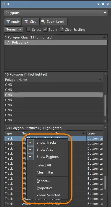
В режиме Polygons панели PCB panel’s три её основные области меняются, отражая иерархию полигонов текущего проекта печатной платы (сверху вниз):
-
Polygon Classes.
-
Отдельные Polygons внутри класса.
-
Отдельные Polygon Primitives, которые составляют полигон.
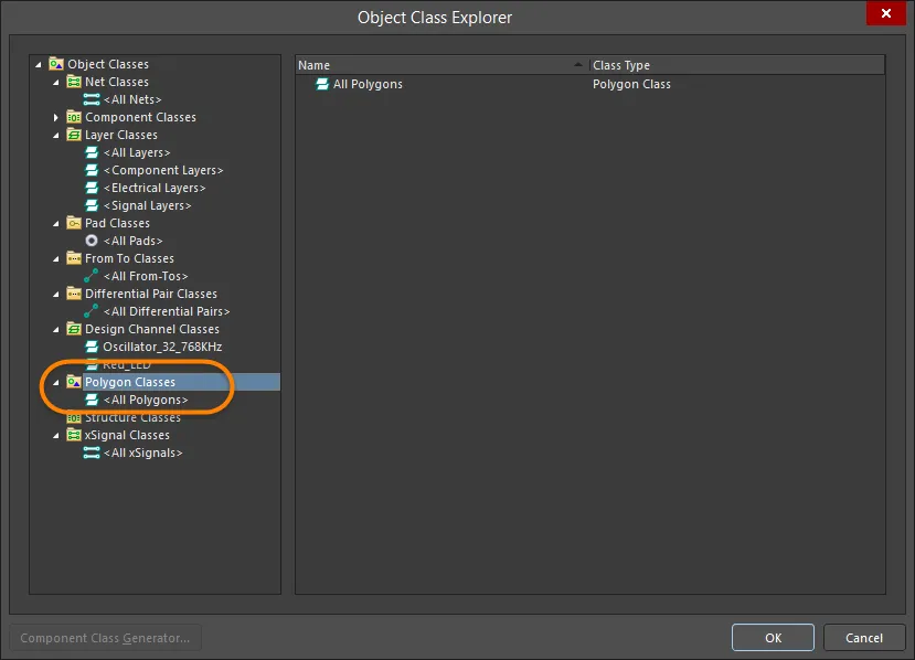
Для полного управления и редактирования классов полигонов откройте диалоговое окно Object Class Explorer dialog с помощью команды Design » Classes в главном меню. В этом диалоговом окне можно просматривать/изменять принадлежность полигонов классу, переименовывать его или добавлять дополнительные классы.
В панели PCB щелчок правой кнопкой по записи полигона и выбор Properties (или двойной щелчок по записи) откроет режим Polygon Pour mode of the Properties panel, где можно просматривать/изменять свойства по мере необходимости. Аналогично, щелчок правой кнопкой по записи примитива полигона и выбор Properties (или двойной щелчок непосредственно по записи) предоставит доступ к соответствующему режиму панели Properties , где можно просматривать/изменять свойства примитива по мере необходимости.
В области Polygon Primitives панели PCB отображение/включение каждого типа примитива полигона зависит от настройки соответствующего разрешающего параметра, доступного из контекстного меню (правый клик).
Отчёты по полигонам
Для получения дополнительной информации о заливках полигонов на вашей печатной плате используйте область Board Information панели Properties (доступна, когда в рабочем пространстве не выбраны объекты) либо выведите список свойств заливки полигона и её дочерних элементов. Количество полигонов, обнаруженных на печатной плате, показано в области Primitives & Others области Board Information . Имейте в виду, что это общее число отражает не только заливки полигонов, но и внутренние плоскости (internal planes) и разделённые плоскости (split planes). Для детального списка свойств полигонов используйте панель PCB List.


 Локализовано с помощью ИИ