从历史上看,PCB 一直是在二维设计空间中进行布局的,通过颜色来表示 PCB 的各个层。然而,实际的 PCB 是一个三维物体,这就要求 PCB 设计人员将屏幕上多层的二维表示,在头脑中映射为三维表示。
3D 显卡以及相关软件技术的显著进步,使 Altium 得以开发出解决这一问题的方案——真正的三维 PCB 编辑。它不仅仅是可视化,Altium Designer 的 3D 功能还允许你:
-
执行 3D 间隙检查——可按需将元件彼此之间以及与外壳进行精确对齐。
-
直观定位连接器及其他需要检修访问的元件。
-
在已考虑所有机械约束的前提下,更好地定义制造流程与装配顺序。
-
使用更接近人眼实际所见的图像,生成更详细的手工装配说明、用户手册和操作说明。
-
尝试不同颜色的阻焊层,以打造更美观、并能与外壳及周边环境更协调的产品。
-
通过向关键干系人展示更具体的最终产品视图,更容易获得他们的支持。

同一区域的电路板 2D 与 3D 视图。
显示模式
Altium Designer 支持以 2D 或 3D 显示并编辑电路板;这些被称为 display modes。在 View 菜单中选择所需模式,或按下 1, 2 或 3 快捷键直接切换到对应模式。
共有三种显示模式,每种都有不同的功能。
 同一块电路板分别以 Board Planning 模式、2D Layout 模式和 3D Layout 模式显示。
视图配置面板
PCB 编辑器设计空间中当前显示的内容以及显示方式,可在 View Configuration 面板中进行配置。这包括层可见性与颜色、对象可见性与透明度、遮罩与变暗级别、当前单层模式,以及若干额外的设计空间显示特性,例如在焊盘、过孔与走线上显示网络名称。

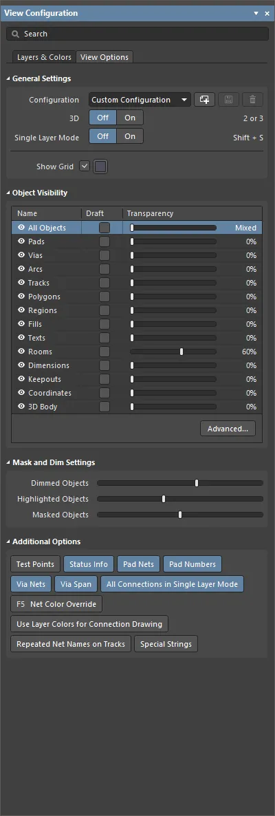
与显示相关的设置在 View Configuration 面板中配置。
除了访问面板的标准方式(通过设计空间右下角的 Panels 按钮或 View » Panels 菜单)之外,还可以使用 View Configuration 面板的 L 或 Ctrl+D 快捷键来访问(分别打开并显示 Layers & Colors 或 View Options 选项卡),或点击设计空间左下角 Layer Sets 控件上的颜色样本( )。
)。
该面板内容分为两个选项卡。点击面板顶部的选项卡以显示该选项卡可用的选项:
可用选项将取决于当前 Layout Mode(2D 或 3D)。
在 3D Layout 模式下,
Section View 选项卡也会在
View Configuration 面板中可用。使用该选项卡来配置 PCB 的剖切视图——
了解更多。
配置层可见性
每一层都可以在 View Configuration 面板的 Layers & Colors 选项卡的 Layers 区域中显示或隐藏。点击可见性图标( )即可切换显示/隐藏。

使用可见性图标管理层可见性
在适用情况下,每个分组也包含一个可见性图标。例如,在上图中:
-
字符串 Component Layer Pairs (C) 左侧的可见性图标用于切换 all 元件层的显示/隐藏。
-
字符串 Top 左侧的可见性图标用于切换 all top side 元件层的可见性。Bottom 侧的层也可以用同样方式显示/隐藏。
Controlling Layer Visibility from the Keyboard
在繁忙的 PCB 设计中,设计过程中经常需要反复打开/关闭各层。为此,可以通过按键以如下方式更改层可见性:
-
按下 L 快捷键以显示/激活 View Configuration 面板的 Layers & Colors 选项卡。面板标题栏会变为彩色,表示它是软件中的活动元素。
-
注意:在某些层及层组名称右侧的圆括号中会有字符或数字,例如 Component Layer Pairs (C) 和 [1] Top (T)。圆括号中的字符/数字就是键盘快捷键。举例来说,先按 L 快捷键使面板处于活动状态,然后按 T 快捷键即可切换 Top 信号层的可见性。
-
如果你已进入某个层组,按 Spacebar 可切换该层组内所有层的可见性。
-
如果你已进入某一层,该层的可见性会立即切换,随后可使用 Spacebar 再次切换。
-
按 Up 或 Down 方向键在列表中向上或向下移动,例如访问某个特定机械层或一对元件层。然后可使用 Spacebar 切换该层/层对的可见性。
-
方括号中的数字表示该信号层或平面层在层叠中对应的物理铜层序号。以字符串 [6] Bottom (B) 为例,[6] 表示这是层叠中的第 6 层铜层,Bottom 是用户在 Layer Stack Manager 中为该层指定的名称,而 (B) 是用于切换该层可见性的快捷键。
-
信号层与平面层的快捷键最多到 (9),即键盘上最后一个可用的数字键。
层集合
层集(Layer Set)是一个已命名的可见层集合。使用 View Configuration 面板的 Layers & Colors 选项卡中 Layers 区域内的 Layers Sets 下拉菜单选择现有层集;显示将更新为仅显示该层集中已启用的层。可以创建任意数量的用户自定义层集,并且也可以编辑当前选中的层集。
-
要创建新的用户自定义层集,请按需在 Layers 区域中定义层可见性,然后单击
 按钮。该集合将以 My Layers 的名称出现在下拉菜单中。之后添加的每个层集都会自动编号。
-
要更改现有用户自定义层集中已启用层的配置,请在 Layers Sets 下拉菜单中选择该层集,按需配置层可见性,然后单击
 按钮以将更改保存到该层集中。
-
要重命名现有用户自定义层集,请在 Layers Sets 下拉菜单中选择它,并在 Layer Sets 字段中输入所需名称。注意:重命名层集不需要执行保存操作,新名称会自动保存。
-
要删除现有用户自定义层集,请在 Layers Sets 下拉菜单中选择它,然后单击
 按钮。
按钮。
-
要从 PCB Layer Set File
(*.layerset) 导入所需层集,或将所需层集导出为 PCB Layer Set File,请分别使用 Import 和 Export 按钮。
使用以下方法切换可见层集:
-
Layer Set View Configuration 面板中的下拉菜单
-
Design » Manage Layer Sets 子菜单
-
Layer Set 控件——通过单击设计空间底部层选项卡左侧按钮的 LS 部分来访问(
 )。
)。
系统颜色
System Colors 区域可用于配置 PCB 上所列项目使用的颜色。颜色与可见性使用常规方法进行配置。
层选项卡
与 View Configuration 面板中当前设置为可见的每个层相关联的选项卡位于设计空间的底部边缘。

它们允许你切换活动层(你将放置对象的层),并直观指示当前正在显示哪些层以及哪个是活动层(高亮的选项卡)。如果层选项卡数量多于一次可显示的数量,请使用箭头  滚动浏览这些选项卡。
层颜色会显示在层选项卡左侧,双击层颜色将打开 Choose Color 对话框。
双击层名称可打开 Edit Layer 对话框,在其中可编辑层名称(以及 internal plane layer 的网络名称)。

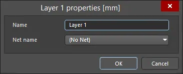
Edit Layer 对话框
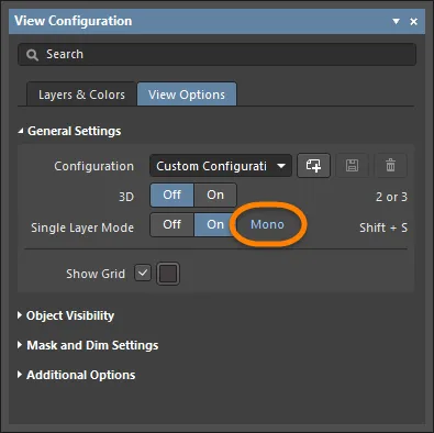
单层模式
单层 2D 显示模式
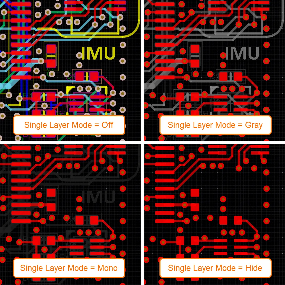
与 Board Insight 集成的是单层(Single-Layer)模式功能,可在 Preferences 对话框的 PCB Editor - Board Insight Display 页面中进行配置。单层模式会显示当前层的内容,同时隐藏或淡化所有其他层的内容。除了隐藏其他所有层上的全部对象、仅显示当前层内容之外,单层模式还提供灰度与单色显示模式。将其他层颜色转换为灰度或单色,可在不分散你对目标层注意力的情况下,保留设计中其他对象位置的空间关系信息。要在完整显示与各个已启用的单层模式之间循环切换,请按 Shift+S 快捷键。每按一次 Shift+S,软件就会切换到下一个已启用模式,最终返回完整显示模式。单层模式在 Preferences 对话框的 PCB Editor - Board Insight Display 页面中启用。禁用(取消勾选)你不希望在按下 Shift+S 时被包含的任何模式。这些设置适用于此 Altium Designer 安装中的所有设计。
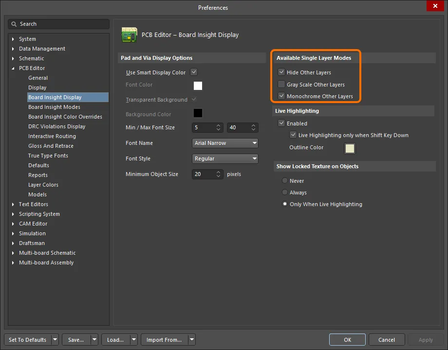
可用的单层模式包括:
-
Hide Other Layers - 隐藏所有其他层;仅显示活动(当前)层的内容。
-
Gray Scale Other Layers - 所有其他层以基于其当前层颜色生成的灰度阴影显示;活动层以其标准颜色显示。
-
Monochrome Other Layers - 所有其他层以相同的灰度阴影显示;活动层以其标准颜色显示。
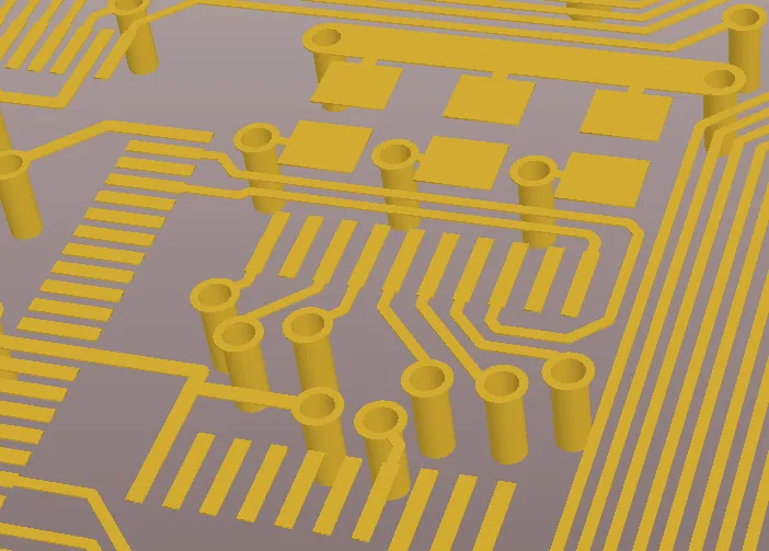
下图展示了常规多层显示以及三种单层显示模式。
当前选择的单层模式会显示在 View Configuration 面板的 View Options 选项卡中的 General Settings 区域。单击模式链接(位于 On 按钮旁)可进入 Preferences 对话框的 PCB Editor - Board Insight Display 页面,在那里按需配置可用的单层模式。
使用 View Configuration 面板的 View Options 选项卡中 Mask and Dim Settings 区域内的 Masked Objects 滑块,控制灰度或单色单层模式下其他层的亮度。
单层 3D 显示模式
当电路板以 3D Layout Mode 显示时,也可使用单层模式。可用于检查特定层的布线质量或电源平面层质量等任务。在单层模式下,使用 Ctrl+Shift+Wheel Roll 快捷键逐层切换。
在单层模式显示中永久显示某一层
要在单层模式显示中包含某一层,请在 View Configuration 面板的 Layers & Colors 选项卡上,对所需层对应的“眼睛”图标执行一次 Ctrl+Click,将该层加入单层模式显示;眼睛图标后方会出现一个方块( ),表示该层将在单层模式中永久显示。
从底面查看电路板
要从底面查看电路板(本质上是翻转电路板),请在 View Configuration 面板的 Layers & Colors 选项卡中 Layers 区域启用 View From Bottom Side 选项,从主菜单选择 View » Flip Board 命令,或使用 Ctrl+F 键盘快捷键。
对翻转后的电路板/元件,所有操作与编辑命令均受支持。坐标空间在逻辑上保持一致,即设计空间原点会从左下角移动到右下角。当前网格位置在 X(水平)方向上,会随着鼠标从右向左移动而增大,而不是正常情况下从左向右增大。视图翻转时生成的任何输出都会保持正确的“从顶视角查看”的坐标信息。
当电路板/元件被翻转时,层的绘制顺序也会通过逻辑配对互换过程发生改变,这意味着 Top Overlay 会在当前层绘制顺序中与 Bottom Overlay 互换位置,Top Layer 与 Bottom Layer 互换,Mid-Layer 1 与 Mid-Layer 30 互换,Internal Plane 1 与 Internal Plane 16 互换,依此类推。机械层的绘制顺序不会改变。
控制对象可见性
除了通过打开/关闭层来控制设计空间中对象的显示之外,另一种方法是基于对象类型来控制对象的可见性与透明度。在 2D Layout 模式下,使用 View Configuration 面板 View Options 选项卡中 Object Visibility 区域提供的选项,按对象类型配置可见性与透明度。

面板 View Options 选项卡中的 Object Visibility 部分
-
– 通过单击相应的可见性图标来控制特定对象类型的可见性。单击 All Objects 可见性图标可切换所有对象的可见性,然后再启用特定对象类型的可见性。
-
Name – 列出所有可进行视觉调整的对象。
-
Draft – 启用后以轮廓方式显示该对象类型。
-
Transparency – 使用滑块调整该对象类型的透明度,或单击数值并在 0 到 100 之间手动输入所需百分比(0% 为完全可见(不透明/实心);100% 为完全透明(不可见))。将对象设为透明意味着你可以看出一个对象何时覆盖另一个对象,例如走线段末端与焊盘相接的位置。
-
Advanced – 单击以打开 Object Visibility 对话框,你可以在其中为某一对象在不同层上设置统一的透明度级别,并为特定层上的不同对象设置不同透明度。
通过在此面板的 General Settings 区域创建自定义配置(Custom Configuration),可轻松恢复你偏好的可见性设置。
遮罩与淡化设置
为帮助管理即使在简单 PCB 设计中也可能存在的大量对象的显示,PCB 编辑器提供了将不感兴趣对象淡化的功能。例如,如果你在 PCB 面板的 Nets 模式下单击某条网络,并且面板下拉选项设置为 Dim 或 Mask,则所有不属于该网络的对象都会被淡化。这样你就能更容易将注意力集中在特定设计元素上,例如某条网络 或某一类网络、某一类元件、被某条设计规则选中的对象等。使用 View Configuration 面板的 View Options 选项卡中 Mask and Dim Settings 区域的滑块来配置遮罩(Masking)与变暗(Dimming)的级别。

View Configuration 面板 View Options 选项卡的 Mask and Dim Settings 区域
管理配置
配置是对层颜色与层可见性设置的预打包定义。在 View Configuration 面板 View Options 选项卡的 General Settings 区域中,从 Configuration 下拉列表选择现有配置,或使用下拉列表旁的按钮创建、保存或删除配置。自定义配置会同时保存当前/上次使用的 2D 与 3D 显示设置。
-
– 单击以创建新的自定义配置,然后输入新名称并单击 按钮。
-
– 在创建新的自定义配置时,或编辑了当前选中的自定义配置后,单击以保存。
-
– 单击以删除当前选中的自定义配置。
-
已创建并保存的自定义配置会自动加载,并可在 Configuration 字段的下拉列表中选择。
-
使用 Configuration 字段下拉列表中的 Load View Configuration 选项,可加载存储在当前 Altium Designer 安装的非标准位置中的配置文件。注意,用户自定义配置会保存为 Complex Configuration(文件扩展名为
.config_complex),因此在加载自定义配置时,你可能需要在 Open 对话框中更改 File Type 下拉选项。
附加选项
View Configuration 面板 View Options 选项卡的 Additional Options 区域提供了用于控制特定元素视图的附加选项。

View Configuration 面板 View Options 选项卡的 Additional Options 部分
-
Test Points – 启用此选项可在已配置为测试点的焊盘与过孔上显示附加信息。可在 Properties 面板相关模式中启用 Fabrication 和/或 Assembly Testpoint 选项,将焊盘或过孔配置为测试点。测试点通过在焊盘/过孔上添加字符串
<Layer> Fab Testpoint 或 <Layer> Assy Testpoint 来标识。
-
Status Info – 启用此选项后,当鼠标悬停在设计空间中的对象上时,会在 Status Bar 中显示坐标位置、层等摘要信息。
-
Pad Nets – 启用此选项可在焊盘上显示关联的网络名称。注意:只有在放大到足够近时网络名称才会可见。
-
Pad Numbers – 启用此选项可显示焊盘编号。注意:只有在放大到足够近时焊盘编号才会可见。
-
Via Nets – 启用此选项可在过孔上显示相关网络名称。注意:只有在放大到足够近时网络名称才会可见。
-
Via Span – 启用此选项可显示过孔允许跨越的层跨度长度。此后,已放置过孔的属性(直径、孔径等)将由设计规则或手动定义。注意:只有在放大到足够近时网络名称才会可见。过孔跨度中的层编号可显示在所有过孔类型内部。
-
All Connections in Single Layer Mode – 启用此选项可在单层模式(Single Layer Mode)下始终显示所有连接线。若禁用此选项,在切换到单层模式时,所有起点或终点不在当前层的连接线也会被隐藏 (因为默认认为它们不相关)。
-
Net Color Override – 每条网络都可以分配一种颜色。要配置颜色,请在 PCB 面板的 Nets 模式下双击该网络名称;将打开 Edit Net dialog 。颜色会自动应用到该网络的连接线 上,并且也可以通过启用此选项将颜色应用到布线。布线颜色会依据 Preferences 对话框中 PCB Editor – Board Insight Color Overrides page 的当前设置来应用:你可以选择 Pattern 选项来定义颜色如何应用,并选择 Zoom Behavior 来定义何时应用颜色。按下 F5 快捷键可切换 Net Color Override 选项的开/关。
-
Use Layer Colors for Connection Drawing – 启用此选项可使用连接线起始层与终止层的颜色来显示连接线。连接线在其起点/终点对象处显示为纯层颜色,并沿连接线长度在两种层颜色之间渐变过渡。该功能在多层板布线时很有帮助,因为它能指示正在布线的连接必须到达的目标层。注意:颜色渐变仅应用于从一层到另一层的连接;如果连接起点与终点在同一层,则会保留分配的网络颜色。
-
Repeated Net Names on Tracks – 启用以在走线上显示重复的网络名称。
-
Special Strings – 启用该选项后,任何由已转换的 Special Strings 生成的已放置字符串(Strings)都会叠加(标注)显示未转换的 Special String 名称。放大某个字符串即可看到其标注叠加层。


 AI 翻译
AI 翻译