Проблема
С ростом скоростей переключения устройств возникает задача сохранения целостности сигнала и соблюдения его временных требований. Целостность сигнала можно обеспечить с помощью трассировки с контролируемым импедансом, которая достигается тщательным проектированием как стека слоёв PCB, так и ширин дорожек, используемых на каждом слое.
Временные требования выполняются за счёт согласования (выравнивания) длин трассируемых путей сигнала. Для набора двухконтактных сигнальных путей, каждый из которых идёт от выходного вывода к одному входному выводу, вычисление и сравнение длин — процесс достаточно простой. Однако для многих типовых проектных решений это не так, поскольку в сигнальном пути может присутствовать компонент последовательного согласования (series termination), либо в сигнале может быть более двух выводов; тогда трассировка может выполняться по топологии Balanced T или Fly-By, как показано на изображении ниже.

Четыре микросхемы DDR2 RAM, трассированные по топологии Balanced T. ##
Решение
Задача проектировщика — преобразовать требования к проекту, например максимально допустимую длину трассы для укладывания в временной бюджет, в набор правил проектирования, таких как правило Length для обеспечения соблюдения тайминга и правило Matched Length для выявления потенциальных рассогласований по времени.
Теперь проектировщик рассматривает сигналы с точки зрения их функции (например: «Этот адресный сигнал должен быть проложен от этого разъёма к каждому устройству памяти. Для этого я выполню трассировку по топологии fly-by с терминатором на конце. Возможно, мне также потребуется последовательный терминатор у источника»). Хотя адрес A0 проходит через терминатор, для проектировщика этот сигнал всё равно остаётся A0 и по другую сторону этого резистора.
Но редактор PCB видит каждый сигнал просто как набор соединённых выводов (обычно называемый цепью, net) — Net A0 идёт от этого вывода разъёма к этому выводу компонента памяти, затем к этому выводу компонента памяти и т. д. Как только добавляется резистор последовательного согласования, эта адресная линия превращается в две отдельные цепи. Это затрудняет для проектировщика задание ключевых требований, таких как правила Length и Matched Length.
Этим можно управлять с помощью функции под названием xSignals (или extended Signal). Эта функция обеспечивает корректную трактовку высокоскоростного сигнального пути именно как пути прохождения сигнала между источником и назначением — через согласующие компоненты, а также через ответвления.
xSignal по сути является определяемым проектировщиком сигнальным путём между двумя узлами. Это могут быть два узла в пределах одной цепи, либо два узла в связанных цепях, разделённых компонентом. Затем xSignal можно использовать для ограничения области действия соответствующих правил проектирования, таких как Length и Matched Length, которые будут соблюдаться при выполнении проектных задач, например при интерактивной подстройке длины.
Создание нового xSignal
xSignal — это определяемый проектировщиком сигнальный путь между двумя узлами; это могут быть два узла в одной цепи или два узла в разных цепях.
xSignals определяются следующими способами:
- Используйте xSignals Multi-Chip Wizard. Это будет наиболее распространённый подход к созданию xSignals и он описан ниже.
Либо используются следующие методы: сначала выбираются интересующие объекты, затем выполняется соответствующая команда:
-
Создать один xSignal на основе выбранных площадок. Выберите требуемую стартовую площадку и конечную площадку (эти площадки могут находиться в разных цепях, если присутствует компонент последовательного согласования). Площадки можно выбирать непосредственно в рабочем поле, либо можно использовать панель PCB в режиме Nets для поиска и выбора площадок (как показано на изображении ниже). После выбора площадок либо щёлкните правой кнопкой по выбранной площадке в рабочем поле и выполните команду xSignals » Create xSignal from Selected Pins, либо щёлкните правой кнопкой по одной из выбранных площадок на панели PCB и выполните команду Create xSignal. Новый xSignal будет отображён в режиме xSignals панели PCB.
При определении xSignal на основе выбранных выводов (площадок посадочного места) перед выполнением команды Create выбирайте только стартовую и конечную площадки.
Имя нового xSignal будет представлять собой комбинацию двух имён цепей, разделённых дефисом. Имя xSignal можно отредактировать в режиме xSignals панели PCB.
Новый xSignal можно добавить в класс xSignal: щёлкните правой кнопкой в области xSignal Classes панели, чтобы создать новый класс и добавить в него элементы.
- Выберите компонент-источник, затем щёлкните правой кнопкой по выбранному компоненту и выберите команду xSignal » Create xSignals between Components в контекстном меню. Откроется диалог Create xSignals Between Components, в котором будет выбран указанный компонент-источник. Диалог описан ниже.
- Выберите один или несколько последовательных компонентов в рабочем поле и затем щёлкните правой кнопкой по одному из выбранных компонентов и выберите команду xSignal » Create xSignals from Connected Nets в контекстном меню. Откроется диалог Create xSignals From Connected Nets. Будут выбраны указанный компонент-источник и цепи, подключённые к этому компоненту. Диалог описан ниже.
- Также возможны ситуации, когда требуется создать xSignal внутри существующего xSignal; в этом случае можно использовать режим xSignal панели PCB. Убедитесь, что в верхней части панели включена опция Select, найдите текущий xSignal, выберите требуемые площадки в разделе xSignal Primitives панели, затем щёлкните правой кнопкой по одной из выбранных площадок в рабочем поле и используйте метод, описанный в шаге 2 этого списка, чтобы завершить процесс.

Выберите две площадки в режиме Nets панели, щёлкните правой кнопкой по одной из выбранных площадок и затем выберите Create xSignal. Обратите внимание, что площадки находятся в разных цепях.
Если стартовая и конечная площадки находятся в одной цепи, xSignal получит имя в формате <NetName>_PPn, где n — следующее доступное целое число, используемое для различения нескольких xSignal, определённых для этой цепи. Если стартовая и конечная площадки находятся в разных цепях, xSignal получит имя в формате <StartNet>_<EndNet>_PPn, где n — следующее доступное целое число, используемое для различения нескольких xSignal, определённых для этой комбинации цепей.
Мастер xSignals Multi-Chip Wizard
xSignals Multi-Chip Wizard используется для создания xSignals между одним компонентом-источником и несколькими целевыми компонентами. Wizard использует компонентно-ориентированный подход к определению потенциальных xSignals — вы выбираете один компонент-источник, интересующие цепи и целевые компоненты, а затем Wizard анализирует все потенциальные пути от компонента-источника к компонентам назначения, проходящие через последовательные пассивные компоненты и по любым ответвлениям. Далее, как проектировщик, вы можете выбрать xSignals, которые нужно сгенерировать, а также при необходимости создать правила проектирования Matched Length. Wizard также может использоваться для автоматического создания xSignals и классов xSignal для ряда различных распространённых интерфейсных и память-ориентированных схем.
В этом Wizard выходной вывод называется Source, а целевой входной вывод называется Destination.
Мастер также является инструментом многократного запуска — из общей «мастер-группы» xSignals, которую вы изначально создаёте на странице xSignal Routes, можно выбрать подмножество, определить классы и правила, затем вернуться к мастер-группе, выбрать другое подмножество, определить для него классы и правила и т. д.
Одно из ключевых достоинств Wizard — удобство совместной работы между Wizard и редактором PCB. Щёлкните по xSignal на любой странице мастера — и соответствующие площадки и любая трассировка будут визуально подсвечены на плате.
На данном этапе мастер не поддерживает автоматическое добавление идентификаторов T-образных соединений, часто называемых tie-points или branch-points. Если в вашем проекте есть трассировка с ответвлениями, рекомендуется:
- Подстроить длину от компонента-источника до пассивного компонента (например, резистора последовательного согласования), если такие есть.
- Подстроить длину в каждой ветви — от T-узла до компонента назначения.
- При необходимости подстроить оставшуюся длину между пассивным компонентом (или от источника, если пассивных компонентов нет) и T-узлом.
Если нужно подстраивать длины только ветвей, создайте пользовательскую точку ветвления, разместив в трассировке в месте T-узла одноплощадочный компонент на одном слое. Дополнительные сведения см. в разделе
Defining the Branch Point in a Balanced T Pattern ниже.
Чтобы открыть xSignals Multi-Chip Wizard, выберите команду Design » xSignals » Run xSignals Wizard в главном меню или щёлкните правой кнопкой в области разводки PCB и затем выберите xSignals » Run xSignals Wizard. Будет показана стартовая страница мастера.

Стартовая страница xSignals Multi-Chip Wizard
xSignals Multi-Chip Wizard Режимы
На второй странице Wizard вам будет предложено выбрать Custom Multi-Component Interconnect, On-Board DDR3 / DDR4 или USB 3.0. Режим Custom Multi-Component Interconnect используется для определения нескольких xSignals между выбранным компонентом-источником и несколькими целевыми компонентами, тогда как режим On-Board DDR3 / DDR4 используется для создания xSignals для памяти DDR3 или DDR4. Режим USB 3.0 создаёт xSignals, классы xSignal и правила Matched Length для каждого канала USB 3.0. Выберите режим, соответствующий вашим задачам.
The Custom Multi-Component Interconnect Mode
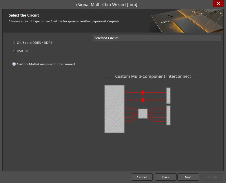
В этом режиме Мастер можно использовать для определения нескольких xSignals между выбранным исходным компонентом и несколькими целевыми компонентами. Мастер использует компонентно-ориентированный подход к выявлению потенциальных xSignals: вы выбираете один исходный компонент, интересующие цепи (nets) и компоненты назначения; затем он анализирует все возможные пути от исходного компонента к компонентам назначения, проходя через последовательные пассивные компоненты и по всем ответвлениям. После этого вы, как разработчик, выбираете xSignals, которые нужно сгенерировать. Помимо определения сквозных (end-to-end) xSignals для нескольких цепей между компонентами, Мастер также позволяет создавать xSignals для участков этих сквозных сигналов (от выходного вывода источника до последовательного терминатора и от последовательного терминатора до входного вывода назначения). В зависимости от включённых настроек Мастер также может создавать классы xSignal и правила проектирования Matched Net Lengths, нацеленные на эти xSignals. Когда работа Мастера завершена, можно приступать к процессу подстройки длины.
Мастер настраивается на нескольких страницах. Количество страниц зависит от конфигурации схемы. Например, при наличии последовательных терминаторов появятся дополнительные страницы. Настройка каждой страницы описана ниже.
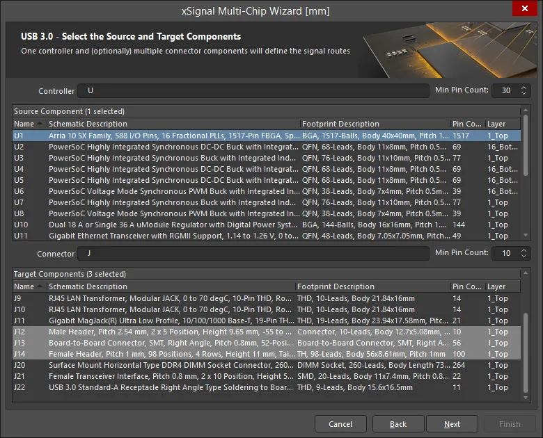
Выбор исходного компонента
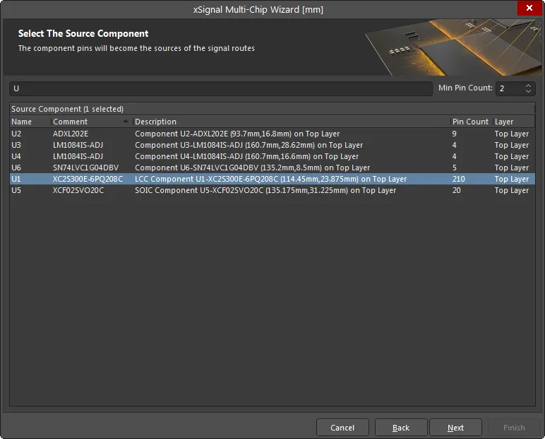
Используйте эту страницу, чтобы выбрать один исходный компонент. Используйте поля Filter и Min Pin Count в верхней части таблицы, чтобы быстрее найти нужный компонент. Поддерживаются подстановочные символы * и ?.
Таблицы в этом Мастере включают контекстное меню по правому клику, а также поддержку стандартных клавиш множественного выбора Windows. Также можно использовать левый клик или пробел, чтобы переключать флажок у выбранных элементов.
Выбор исходных цепей (Source Nets)
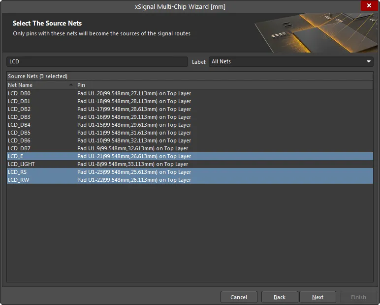
Выберите интересующие цепи, подключённые к выбранному исходному компоненту. Используйте поля Filter и Label в верхней части таблицы, чтобы быстрее найти нужные цепи. Источниками маршрутов сигналов станут только выводы с перечисленными цепями.
Выбор компонентов назначения
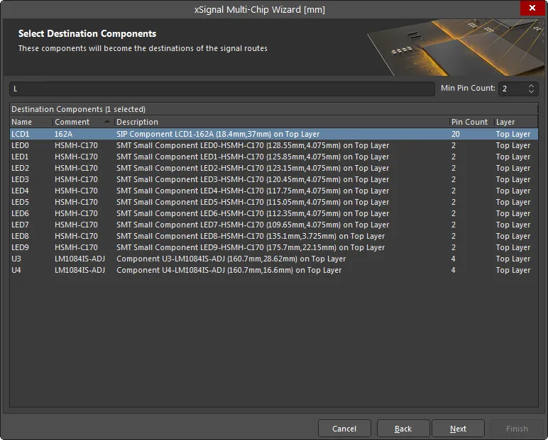
Выберите нужный(е) компонент(ы) назначения. Используйте поля Filter и Min Pin Count в верхней части таблицы, чтобы быстрее найти нужный компонент.
Когда вы нажмёте Next, Мастер определит все возможные xSignals, которые можно создать из набора выбранных цепей между выбранными компонентами. Если Мастер обнаружит 2-выводные компоненты, у которых оба вывода подключены к выбранным цепям, они автоматически будут определены как последовательные терминаторы, и позже в процессе появятся дополнительные страницы Мастера.
Маршруты xSignal
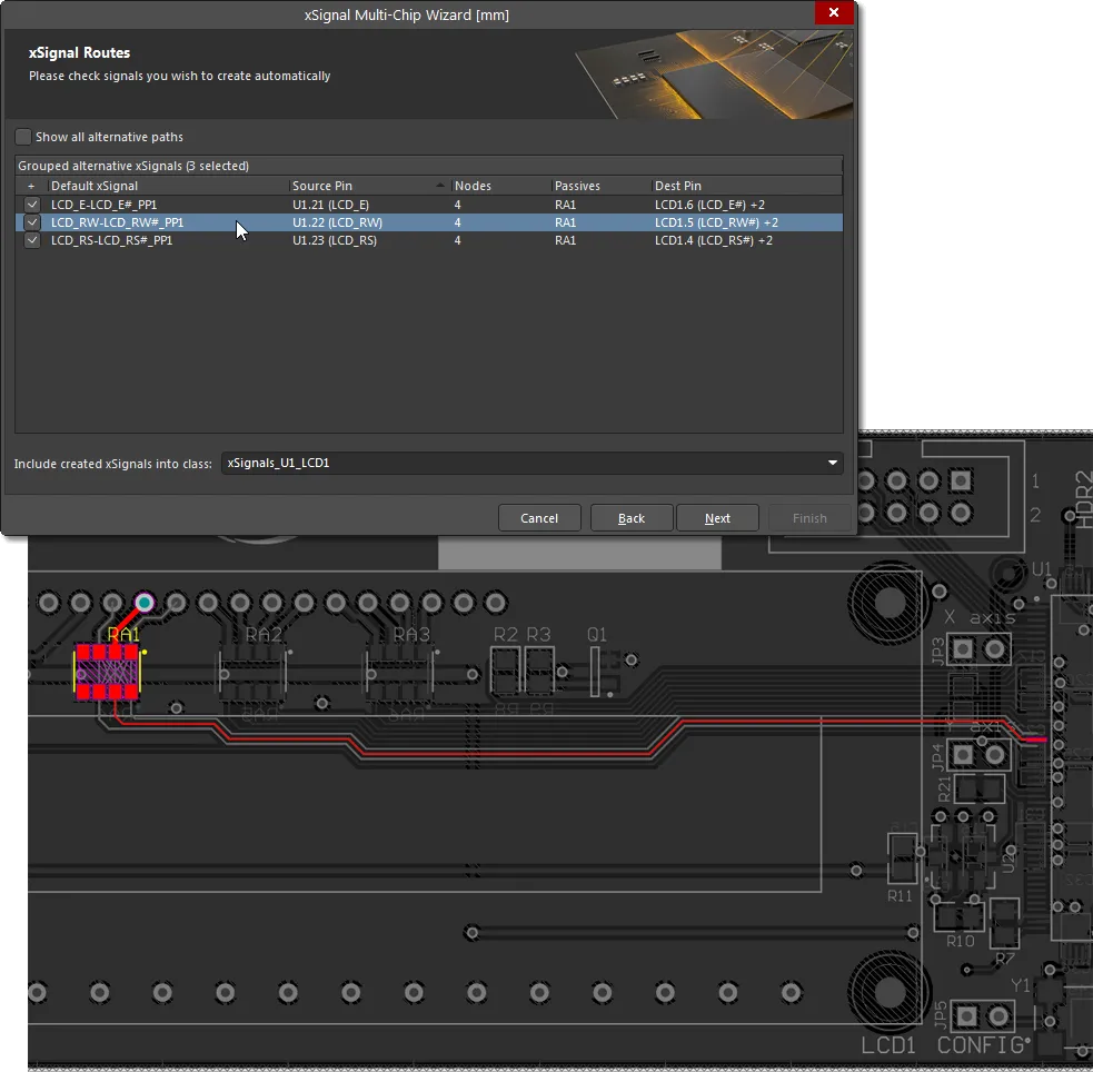
На этой странице Мастера перечислены предлагаемые xSignals от каждого Source Pin до каждого Destination Pin. Щёлкните по записи, чтобы подсветить соответствующий xSignal на плате.
После анализа путей цепей для выявления потенциальных xSignals Мастер попытается сократить набор, чтобы показывать только те комбинации, которые вам интересны. Это сквозные (end-to-end) xSignals; на изображении выше они показаны между исходным и целевыми компонентами, выбранными на предыдущих страницах Мастера. На изображении также видно, что Мастер обнаружил последовательный терминатор RA1 в каждом маршруте. RA1 на самом деле — сборка из четырёх резисторов; в такой ситуации Мастер автоматически создаст логические соответствия, предполагая, что каждый резистор проходит «поперёк» сборки, и сопоставит цепи, подключённые к выводам, расположенным напротив друг друга на компоненте.
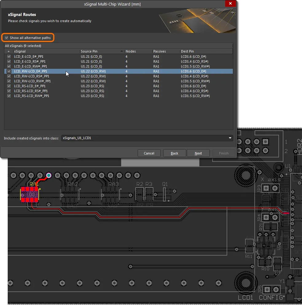
Поскольку предположение о том, что выводы каждого резистора расположены напротив друг друга, не всегда может быть верным, вы можете выбрать любую другую доступную исходящую цепь через выпадающий список в столбце Dest Pin. Либо включите опцию Show all alternative paths в верхней части таблицы, чтобы отобразить все потенциальные комбинации цепей, которые можно использовать для генерации xSignals. Установите флажок для каждой строки, для которой нужно создать xSignal. Включённые xSignals будут добавлены в класс, отображаемый в поле Include created xSignals into class внизу этой страницы. Введите новое имя или выберите его из выпадающего списка.
Подстройка длины xSignals
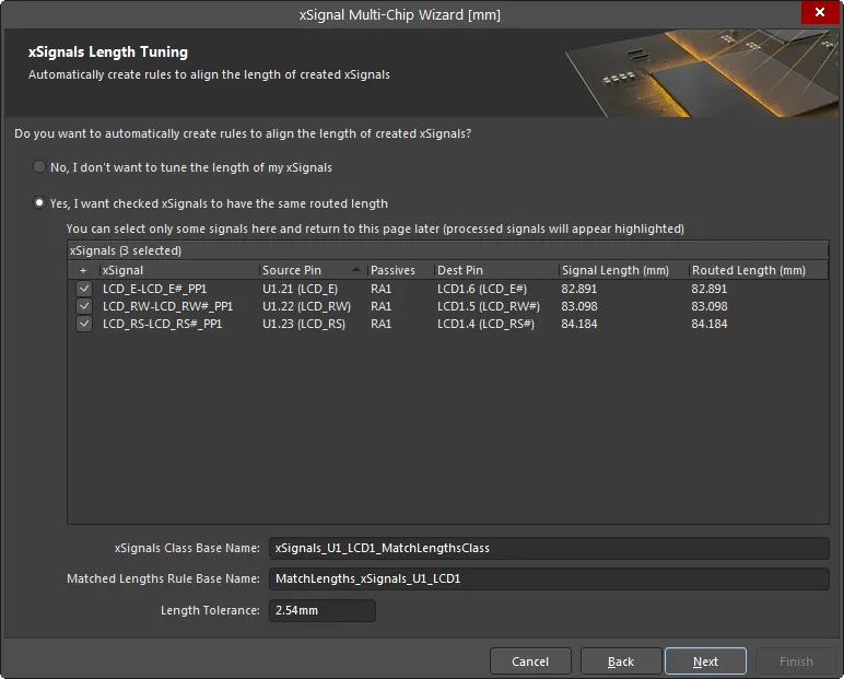
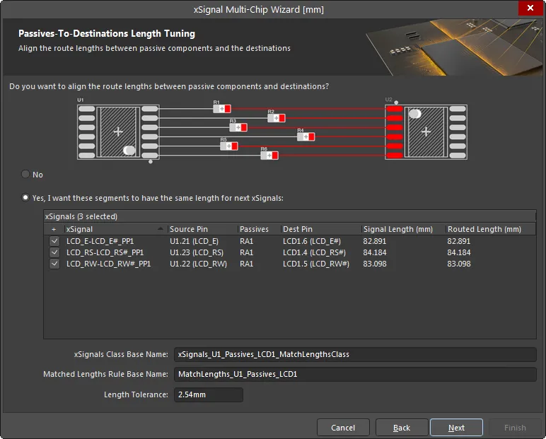
Эта страница используется для автоматического создания правила проектирования Matched Length для включённых xSignals. Включите only те xSignals, на которые должно распространяться это новое правило. Если в проекте требуется несколько правил с разными требованиями, позже в процессе вам будет предоставлена возможность определить дополнительные правила для тех xSignals, для которых правило ещё не задано . На этом первом этапе также будут представлены сквозные (end-to-end) xSignals. На последующих страницах Мастера у вас будет возможность определить правила проектирования для участков внутри xSignals — например, для участков от выходного вывода до последовательного терминатора.
Если вы не хотите подстраивать длину ваших xSignals, включите No, I don't want to tune the length of my xSignals. При включении этой опции другие параметры на странице будут недоступны. Чтобы иметь возможность редактировать и использовать остальные параметры, включите Yes, I want checked xSignals to have the same routed length.
Поле xSignals Class Base Name используется для задания имени для текущего выбранного набора xSignals. Введите осмысленное имя, учитывая, что вы можете повторять этот процесс для других xSignals. Затем на этот набор xSignals будет нацелено правило проектирования с именем, которое вы введёте в поле Matched Lengths Rule Base Name, с указанным Length Tolerance.
Не уверены, какие объекты попадают под действие? Щёлкните по одной или нескольким записям, чтобы подсветить путь(и) сигнала в топологии PCB.
Подстройка длины от источника до пассивов
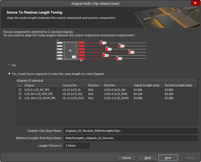
Если выбранный набор цепей включает последовательные терминаторы, появятся дополнительные страницы Мастера, которые дадут возможность создать дополнительные xSignals и правила проектирования для этих участков цепей. На изображении выше показано, что эта страница Мастера используется для создания правила Matched Length для выбранных xSignals, идущих от выводов источника к терминаторам. Если для этого требуются xSignals / класс xSignal / правило проектирования, включите опцию Yes, I want these segments to have the same length for next xSignals, включите нужные xSignals и задайте xSignals Class Base Name, Matched Lengths Rule Base Name и Length Tolerance. Для использования с этим правилом Matched Length будут созданы дополнительные xSignals.
Подстройка длины от пассивов до назначений
Эта страница используется для создания правила Matched Length для выбранных xSignals, идущих от терминаторов к выводам назначения. Если это требуется, включите опцию Yes, I want these segments to have the same length for next xSignals , включите нужные xSignals и задайте xSignals Class Base Name, Matched Lengths Rule Base Name и Length Tolerance. Для использования с этим правилом Matched Length будут созданы дополнительные xSignals.
Отчёт и продолжение
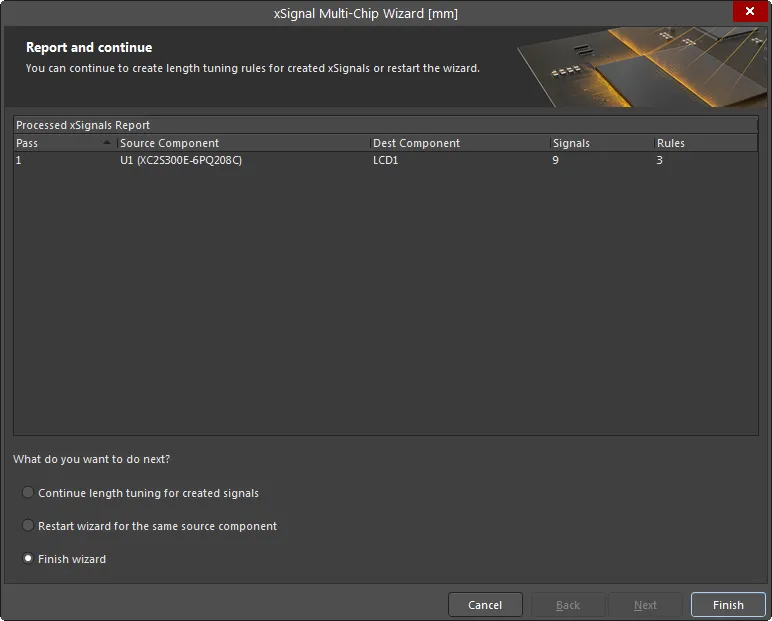
На этой странице Мастера будет указано количество xSignals, которые будут созданы, и количество правил проектирования, которые будут созданы.
Внизу страницы можно выбрать:
- Continue length tuning for created signals – выбрать, если вы отключили определённые xSignals на предыдущих страницах и теперь нужно пройти процесс определения дополнительных правил для этих xSignals.
- Restart wizard for the same source component – выбрать, если вы хотите отбросить эти настройки и перезапустить Мастер с теми же выбранными компонентами/цепями.
- Finish wizard – выбрать, если вы завершили создание xSignal и правил проектирования для этого исходного компонента.
xSignals подробно отображаются в режиме xSignal панели PCB. Нажмите клавишу Delete в панели, чтобы удалить выбранные классы xSignal или выбранные xSignals.
Эти xSignals готовы к подстройке длины. Чтобы начать, выберите опцию Interactive Length Tuning ( ) в главном меню Route или в Active Bar.
Вы можете легко удалить «гармошку» подстройки длины. Один раз щёлкните по любому сегменту «гармошки», чтобы выбрать её, затем нажмите Delete.
Обратите внимание: при размещении «гармошки» существующие сегменты дорожек разрываются в начальной и конечной точках. Поэтому, если повторить процесс «подстроить—удалить» несколько раз, можно получить прямой участок трассировки, который фактически состоит из множества коротких сегментов дорожек. Чтобы объединить множество мелких сегментов обратно в один сегмент, выполните команду Design » Netlist » Clean All Nets из главных меню.
On-Board DDR3 / DDR4
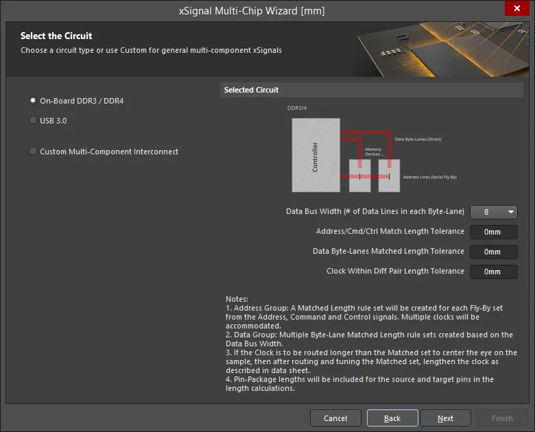
В этом режиме мастер автоматически создаст xSignals, классы xSignal, Matched Length Groups, правила Diff Pair Matched Lengths и топологию Fly-By для встроенной (on-board) DDR3/DDR4. Мастер предполагает, что будет использоваться топология трассировки fly-by.
Выбор исходных компонентов
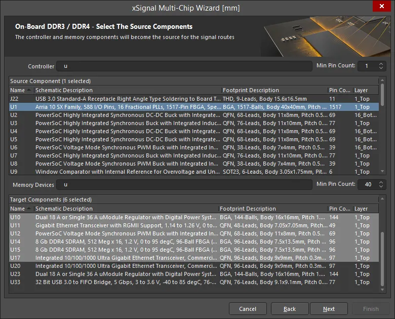
На этой странице Wizard определяет все потенциальные исходные и целевые компоненты на основе префикса позиционного обозначения и количества выводов. Используйте поля Controller/Memory Devices для фильтрации компонентов/микросхем памяти и используйте стрелки вверх/вниз, чтобы задать Min Pin Count требуемым образом как для Source Component, так и для Target Components Затем выберите один исходный компонент и выберите целевой(е) компонент(ы).
Группа адреса (Address Group)
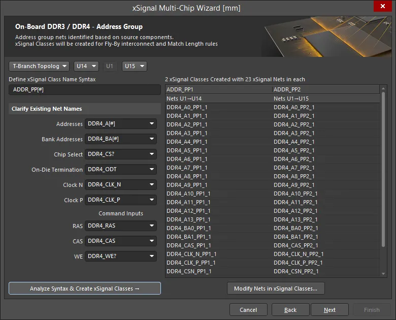
Функциональность этой страницы следующая:
- Fly-By TopologyПоддерживаются опции T-Branch Topology и T-Branch Topology. Выберите требуемую топологию из выпадающего списка.
- Если выбрано Fly-By Topology, целевые устройства перечисляются в порядке Point-to-Point для fly-by трассировки. Программа попытается определить порядок автоматически. Если Мастер запускается до размещения компонентов, порядок point-to-point нужно будет задать вручную с помощью выпадающих элементов управления.
- Если выбрано T-Branch Topology (как показано выше), половина целевых устройств будет показана перед источником, а половина — после. Используйте выпадающие элементы управления, чтобы упорядочить целевые компоненты нужным образом.
- Define xSignal Class Name Syntax:
- Начальное значение по умолчанию —
ADDR_PP[#]
- Параметр
[#] представляет количество микросхем памяти.
- Суффикс
PP при необходимости можно изменить.
- Мастер анализирует компоненты, ищет эти суффиксы в проекте и отображает полный синтаксис имени, используя подход, описанный ниже. Обновите их, если они указаны неверно.
- Цель здесь — автоматически найти цепи (nets), соответствующие этим функциям. После того как цепи найдены, синтаксис именования вводится в поля.
- Затем просматриваются цепи между компонентами; как только найден суффикс, определяется префикс. Например, Мастер ищет
_A[#], чтобы определить адресные линии.
- Если цепей с суффиксом, начинающимся с «_», не найдено, он ищет только текст после «_». Также проверяются альтернативные разделители, такие как «-» или «.».
- Если синтаксис не удаётся определить автоматически, необходимо задать эти поля вручную. Используйте выпадающие списки, чтобы выбрать из существующих цепей на плате.
- После того как порядок и синтаксис именования определены, нажмите кнопку Analyze Syntax & Create xSignal Classes, чтобы сформировать список xSignals. Мастер проанализирует синтаксис и то, как соединены компоненты, и сформирует классы xSignal, которые отображаются в таблице справа в диалоге. Количество Classes Created будет соответствовать количеству устройств памяти.
- Отображаются количество созданных классов (например, 4) и количество цепей xSignal в каждом классе (например, 26).
- xSignals группируются в отдельном столбце для каждого класса xSignal. Для каждого класса будет создано правило проектирования Matched Lengths. Подзаголовки в таблице представляют исходный и целевой компоненты для этих xSignals.
- Если автоматически сгенерированный список неполный или неверный, нажмите кнопку Modify Nets in xSignal Classes, чтобы открыть диалог Edit xSignal Class и вручную добавить или удалить цепи в/из класса. Учтите, что ручные изменения будут потеряны, если затем снова нажать кнопку Analyze Syntax & Create xSignal Classes.
Определение цепей группы данных (Data Group)
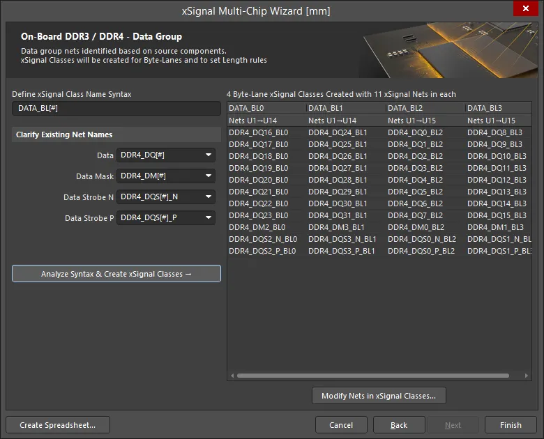
Заключительный этап — определить все цепи, относящиеся к группе данных (Data Group).
Функциональность этой страницы следующая:
- Пользовательский синтаксис имени класса xSignal:
- Начальное значение по умолчанию —
DATA_BL[#]
- .
[#] представляет количество Byte-Lane, которое определяется как общее число линий данных, делённое на ширину шины данных (Data Bus Width), заданную ранее.
- Суффикс
BL при необходимости можно изменить.
- Мастер анализирует компоненты и ищет эти суффиксы в проекте, затем отображает полный синтаксис имени. Если это неверно, используйте выпадающие списки для корректировки.
- После определения синтаксиса именования нажмите кнопку Analyze Syntax & Create xSignal Classes, чтобы сформировать список xSignals. Мастер проанализирует синтаксис и то, как соединены компоненты, и сформирует классы xSignal, которые отображаются в таблице справа в диалоге. Количество созданных классов будет соответствовать числу Byte-Lane, подключённых к устройствам памяти. Над областью таблицы отображаются количество созданных классов (например, 8) и количество цепей xSignal в каждом классе (например, 11).
- Для этих классов xSignal создаются правила проектирования Matched Lengths. Подзаголовки в таблице представляют исходный и целевой компоненты для xSignals Byte-Lane.
- Если автоматически сгенерированный список неполный или неверный, нажмите кнопку Modify Nets in xSignal Classes, чтобы открыть диалог Edit xSignal Class и вручную добавить или удалить цепи в/из класса. Учтите, что ручные изменения будут потеряны, если затем снова нажать кнопку Analyze Syntax & Create xSignal Classes.
- Нажмите кнопку Create Spreadsheet, чтобы сформировать таблицу в формате XLS со списком xSignals, созданных Мастером.
Созданные xSignals и классы xSignal
Мастер автоматически создаёт xSignals и классы xSignal для:
- Адресных xSignals, описанных на странице Address Group.
- Данных xSignals, описанных на странице Data Group.
USB 3.0
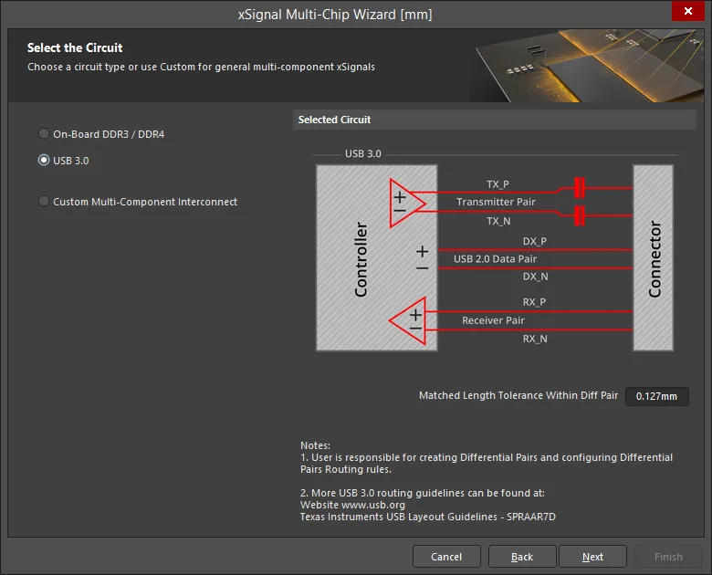
Мастер может обработать все каналы USB 3.0 между каждой парой «контроллер–разъём», заданной пользователем. Мастер автоматически оценивает цепи дифференциальных пар, подключённые к контроллеру, определяя те, которые проходят до разъёма. Протяжённость может включать пассивные компоненты и несколько цепей. Мастер идентифицирует каждую из этих пар классом xSignal, при этом каждое плечо пары определяется xSignal «контроллер–разъём».
После выбора USB 3.0 на странице появится настройка для Matched Length Tolerance Within Diff Pair. Введите подходящее значение. Это значение используется для правила проектирования, создаваемого Мастером, и может быть изменено в любое время в PCB Rules and Constraints Editor. Пользовательские настройки такого типа сохраняются для будущего использования.
Для USB 3.0 каждый пользовательский порт USB называется channel. Как видно на изображении, каждый канал включает три дифференциальные пары: Transmit, Receive и Data.Для USB 3.0 критическое требование к трассировке — согласование длин трасс внутри каждой пары; согласование длин между парами не столь критично. Из‑за этого требования и того факта, что правило Matched Length требует наличия дифференциальных пар для проверки длин внутри пары цепей, Мастер проверит определения Differential Pair и автоматически создаст подходящие дифференциальные пары, если их нет. Затем правило Matched Length, создаваемое Мастером, настраивается на проверку согласования длины Within Differential Pair Length. Обратите внимание: правило настроено на сравнение длин плеч внутри пары для общего xSignal; оно не сравнивает длины плеч внутри каждой дифференциальной пары.
Выбор исходных и целевых компонентов
На этой странице Мастер определяет все потенциальные исходные компоненты и целевые разъёмы на основе префикса позиционного обозначения и количества выводов.
- Задайте префикс фильтра для позиционного обозначения Controller, позиционного обозначения Connector и значения Min Pin Count по необходимости.
- Выберите один исходный компонент.
- Выберите целевой компонент(ы).
Если вы выбираете несколько целевых компонентов, следует проверить синтаксис именования xSignal и цепей для каждого из этих компонентов, используя выпадающий список на следующей странице Мастера.
Каналы: определение групп дифференциальных пар
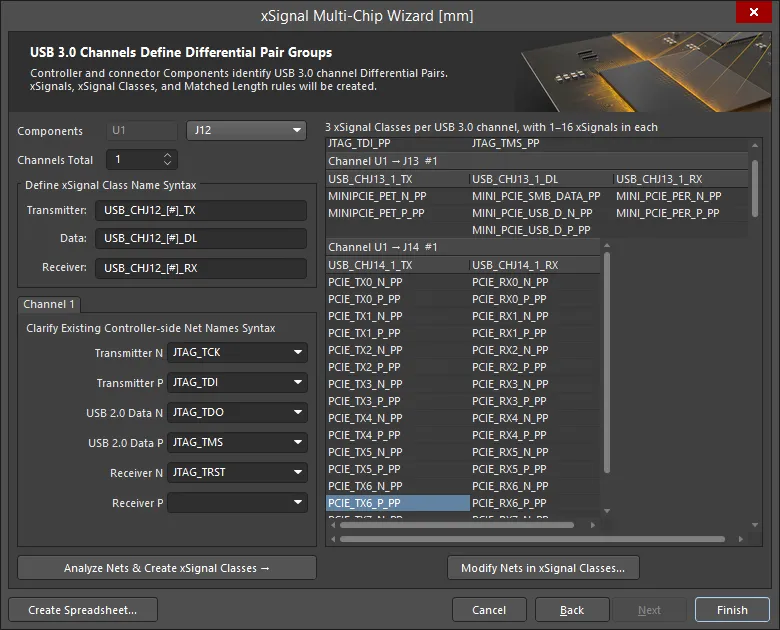
На этой странице задайте синтаксис именования, который Мастер сможет использовать для определения соответствующих цепей пар Transmitter, Receiver и Data, которые затем включаются в xSignals. Каждая пара xSignals затем объединяется в класс xSignal, и эти классы используются для задания области действия правила Matched Length.
Функциональность этой страницы следующая:
- Позиционное обозначение контроллера отображается рядом с меткой Components. Рядом выпадающий список содержит все Connectors, выбранные на предыдущей странице Мастера.
- Показанные параметры синтаксиса именования применяются к каждому разъёму, перечисленному в выпадающем списке. Выбирайте их по очереди и проверяйте, что выбранный синтаксис именования полный и подходит.
- Как упоминалось, для USB 3.0 каждый пользовательский порт USB называется channel. Можно задать количество каналов (Channels Total) от 1 до 32. Обычно каждый разъём имеет один канал.
- Внутри каждого канала USB 3.0 есть три тракта дифференциальных пар: Transmit, Receive и Data, которые идут от контроллера к разъёму. Мастер создаст xSignal (при необходимости охватывая последовательные компоненты) для каждой положительной цепи и ещё один xSignal для каждой отрицательной цепи, а затем класс xSignal, представляющий эту пару «контроллер–разъём». Группа Define xSignal Class Name Syntax используется для задания имён этих классов xSignal. Мастер также создаёт подходящие Differential Pairs, если они ещё не определены.
- Define xSignal Class Name Syntax – создаваемые классы xSignal будут именоваться согласно заданию, при этом каждому каналу будет присвоено числовое значение вместо
[#]. Введите предпочитаемую строку при необходимости.
- Channel <N> – эти поля задают маски, используемые для определения соответствующих имён цепей Transmitter / Receiver / Data.
- У Мастера есть большой шаблон предопределённых схем именования, которые он проверяет и обычно заполняет эти поля автоматически. Если этого не произошло, выберите правильное имя из выпадающего списка или введите подходящий синтаксис имени цепи.
- После настройки полей именования нажмите кнопку Analyze Nets & Create xSignal Classes.
- Мастер создаст xSignals, классы xSignal и правила Matched Length для всех каналов. Обратите внимание: они создаются каждый раз при повторном запуске Мастера. Удалите их, если планируете запускать Мастер снова.
- Итоговые имена классов xSignal и входящие в них xSignals приведены в таблице.
- Нажмите кнопку Create Spreadsheet, чтобы сформировать таблицу в формате XLS со списком xSignals, созданных Мастером.
- Нажмите Finish, чтобы завершить работу Мастера.
Диалог Create xSignals Between Components
Если нужно определить большое количество xSignals, эффективнее использовать диалог Create xSignals Between Components. Он вызывается командой Design » xSignals » Create xSignals; в диалоге представлены исходные и целевые компоненты и можно создать один или несколько xSignals за одну операцию.

Используйте этот диалог, чтобы быстро определить и создать несколько xSignals и добавить их в требуемый класс xSignal.
Подход следующий:
- Выберите один Source Component.
- Выберите один или несколько требуемых Destination Components.
- Выберите интересующий Source Net(s). Будут перечислены все цепи, которые в данный момент подключены к выбранному исходному компоненту. Для цепей, связанных с определённым классом, выберите этот класс в выпадающем списке Net Class.
- Нажмите кнопку Analyze. Программа пытается определить потенциальные xSignals, существующие между выбранными исходным и целевым компонентами для выбранных цепей. Все возможные xSignals, включающие выбранные цепи и проходящие между выбранными исходным и целевым компонентами, будут перечислены в поле xSignals. Обратите внимание: алгоритм анализа следует текущей топологии выбранных цепей, и это будет влиять на предлагаемые xSignals.
ПО также может при необходимости выполнять поиск через последовательные компоненты, выбрав соответствующий параметр в раскрывающемся списке Analyze: Search for direct connections, Through 1 series component, Through 2 series components или Multipath coupled nets.
- После выполнения анализа потенциальные xSignals будут перечислены в нижней части диалога, и все они будут включены для создания. Внимательно просмотрите список предлагаемых xSignals и оставьте включёнными только те, которые действительно нужны. Для переключения состояния сразу нескольких записей используйте команды контекстного меню (правый щелчок).
- Выберите требуемый class в нижней части диалога или введите имя, чтобы создать новый класс. Если класс не выбран, xSignals всё равно будут созданы, и вы сможете добавить их в любой класс xSignal в диалоге Object Class Explorer (Design » Classes). Использование классов может значительно упростить создание и настройку правил проектирования.
- Нажмите OK, чтобы создать xSignals.
Диалог закроется, и вы вернётесь в рабочее пространство проектирования. Новые xSignals будут перечислены в режиме xSignals панели PCB.
Используйте фильтры над каждым списком, чтобы быстро находить нужные компоненты или цепи; поддерживаются подстановочные символы.
Диалог Create xSignals From Connected Nets
Если вы создаёте xSignals, включающие последовательные согласующие (termination) компоненты, хорошим подходом будет использование команды Create xSignals from connected nets. Команда доступна, когда выбран компонент — либо через подменю Design » xSignals в главном меню, либо через подменю xSignals в контекстном меню (правый щелчок).
Эта команда предназначена для построения xSignals «наружу» от выбранного последовательного согласующего компонента, например резистора или конденсатора. Поддерживаются как один или несколько дискретных компонентов, так и один или несколько многосекционных компонентов пакетного типа, например резисторные сборки. После запуска этой команды откроется диалог Create xSignals From Connected Nets.

Используйте диалог для создания xSignals, проходящих через выбранный последовательный компонент. В этом примере предложены два возможных xSignals, но будет создан только один.
Подход следующий:
- Выберите один Source Component.
- Выберите интересующий Source Net(s). Будут перечислены все цепи, которые в данный момент подключены к выбранному исходному компоненту. Для цепей, связанных с определённым классом, выберите этот класс в раскрывающемся списке Net Class.
- Нажмите кнопку Analyze. ПО пытается определить потенциальные xSignals, существующие для выбранных исходных компонентов и для выбранных цепей. Все возможные xSignals будут перечислены в поле xSignals.
- После выполнения анализа потенциальные xSignals будут перечислены в нижней части диалога, и все они будут включены для создания. Внимательно просмотрите список предлагаемых xSignals и оставьте включёнными только те, которые действительно нужны. Для переключения состояния сразу нескольких записей используйте команды контекстного меню (правый щелчок).
- Выберите требуемый class в нижней части диалога или введите имя, чтобы создать новый класс. Если класс не выбран, xSignals всё равно будут созданы, и вы сможете добавить их в любой класс xSignal в диалоге Object Class Explorer (Design » Classes). Использование классов может значительно упростить создание и настройку правил проектирования.
- Нажмите OK, чтобы создать xSignals.
Диалог закроется, и вы вернётесь в рабочее пространство проектирования. Новые xSignals будут перечислены в режиме xSignals панели PCB.
Используйте фильтры над каждым списком, чтобы быстро находить нужные компоненты или цепи; поддерживаются подстановочные символы.
Роль топологии цепи
Когда вы определяете xSignal, он задаётся между двумя узлами или площадками. Однако при выборе этого xSignal в режиме xSignals панели PCB он фактически будет следовать по траектории линий соединения между этими двумя площадками, показывая путь, по которому ПО предполагает трассировку xSignal. Это происходит потому, что соблюдается топология, заданная для данной цепи. Топология цепи определяется применимым правилом проектирования Routing Topology; топология по умолчанию — Shortest.
Простая анимация показывает CPU, подключённый к четырём микросхемам памяти DDR3, которые будут трассироваться по стратегии fly-by. Класс xSignal DRAM_A2 содержит четыре xSignals. Сначала выбирается класс, затем по очереди выбирается каждый xSignal. Видно, как путь xSignal следует топологии цепи, которая сейчас установлена по умолчанию — Shortest.

Поскольку топология цепи сейчас установлена в Shortest, xSignals не следуют требуемому пути от процессора к микросхемам памяти.
Если вы планируете использовать диалог Create xSignals Between Components, вам потребуется настроить топологию цепи(ей), чтобы алгоритм анализа xSignal понимал предполагаемый путь трассировки xSignal.
Команды создания xSignal
Помимо команды Design » xSignals » Create xSignals, в подменю xSignals доступны и другие команды создания xSignal при выполнении определённых условий.
Ниже приведено краткое описание команд и условий их доступности:
| Команда |
Описание |
| Create xSignal from selected pins |
Немедленно создаёт один xSignal . Эта команда доступна, когда в рабочем пространстве выбраны две или более площадки, и совпадает с командой, которая появляется при щелчке правой кнопкой по одной из выбранных площадок.
|
| Create xSignals between components |
Эта команда доступна, когда в рабочем пространстве выбраны компоненты. При её запуске открывается диалог Create xSignals Between Components с предварительно выбранными компонентами. Убедитесь, что выбраны правильные компоненты Source и Designation, затем завершите процесс анализа/создания.
После запуска команды откроется диалог Create xSignals Between Components dialog. Используйте диалог для создания xSignals следующим образом:
- Выбранный исходный компонент будет отображаться выбранным в области Source Component.
- Любые другие компоненты, выбранные в рабочей области, будут отображаться выбранными в области Destination Components. Если нет — выберите их сейчас.
- По умолчанию будут выбраны все цепи, связанные с площадками исходного компонента (в области Source Component Nets). При необходимости скорректируйте выбор.
-
Нажмите кнопку Analyze — ПО попытается определить потенциальные xSignals, существующие между выбранными исходным и целевыми компонентами, для выбранных цепей.
Обратите внимание: алгоритм анализа следует текущей топологии выбранных цепей.
ПО также может при необходимости выполнять поиск через последовательные компоненты, выбрав соответствующий режим из раскрывающегося меню, связанного с этой кнопкой. Доступные режимы: Search for direct connections, Through 1 series component, Through 2 series components и Multipath coupled nets.
- Все найденные xSignals перечисляются в области xSignals диалога. По умолчанию все они выбраны для создания — при необходимости измените это.
- При желании можно связать создаваемые xSignals с классом xSignal. Либо выберите существующий класс xSignal, либо введите имя нового класса. При желании поле можно оставить пустым; xSignals всегда можно добавить в нужный класс позже.
- Нажмите OK , чтобы создать xSignals. Диалог закроется, и вы вернётесь в рабочее пространство проектирования, где будет показан отфильтрованный вид с только что созданными xSignals. Если был указан класс xSignal, он будет создан (если ещё не существует), а xSignals будут связаны с ним.
|
| Create xSignals from connected nets |
Используйте эту команду, когда нужно создать xSignals для одного или нескольких последовательных согласующих компонентов. Выберите согласующий(ие) компонент(ы), затем запустите команду, чтобы открыть диалог Create xSignals from Connected Nets, готовый к завершению процесса создания набора xSignals. Используйте диалог для создания xSignals следующим образом:
- Выбранные исходные компоненты будут отображаться выбранными в области Source Component.
- По умолчанию будут выбраны все цепи, связанные с площадками исходных компонентов (в области Source Component Nets). При необходимости скорректируйте выбор.
-
Нажмите кнопку Analyze — ПО попытается определить потенциальные xSignals, существующие для выбранных цепей, исходящих от выбранных компонентов.
Обратите внимание: алгоритм анализа следует текущей топологии выбранных цепей.
- Все найденные xSignals перечисляются в области xSignals диалога. По умолчанию все они выбраны для создания — при необходимости измените это.
- При желании можно связать создаваемые xSignals с классом xSignal. Либо выберите существующий класс xSignal, либо введите имя нового класса. При желании поле можно оставить пустым; xSignals всегда можно добавить в нужный класс позже.
- Нажмите OK , чтобы создать xSignals. Диалог закроется, и вы вернётесь в рабочее пространство проектирования, где будет показан отфильтрованный вид с только что созданными xSignals. Если был указан класс xSignal, он будет создан (если ещё не существует), а xSignals будут связаны с ним.
|
| Create xSignals |
Открывает диалог Create xSignals Between Components. Эта команда доступна всегда. Используйте диалог для создания xSignals следующим образом:
- Выберите исходный компонент в области Source Component.
- Выберите один или несколько целевых компонентов в области Destination Components.
- Все цепи, связанные с площадками исходного компонента, будут перечислены в области Source Component Nets. Выберите интересующие цепи.
-
Нажмите кнопку Analyze — ПО попытается определить потенциальные xSignals, существующие между выбранными исходным и целевыми компонентами для выбранных цепей.
Обратите внимание: алгоритм анализа следует текущей топологии выбранных цепей.
При необходимости программное обеспечение также может выполнять поиск по компонентам серии — для этого выберите соответствующий режим в выпадающем меню, связанном с кнопкой. Доступные режимы: Search for direct connections, Through 1 series component, Through 2 series components и Multipath coupled nets.
- Все найденные xSignals перечислены в области xSignals диалога. По умолчанию все они выбраны для создания — при необходимости измените выбор.
- При желании можно связать создаваемые xSignals с классом xSignal. Либо выберите существующий класс xSignal либо введите имя нового класса. При желании поле можно оставить пустым; xSignals всегда можно добавить в нужный класс позже.
- Нажмите OK , чтобы создать xSignals. Диалог закроется, и вы вернетесь в рабочее пространство, где будет показан отфильтрованный вид с только что созданными xSignals. Если был указан класс xSignal, он будет создан (если не существовал) и xSignals будут связаны с ним.
|
Определение точки ветвления в сбалансированном T-образном шаблоне
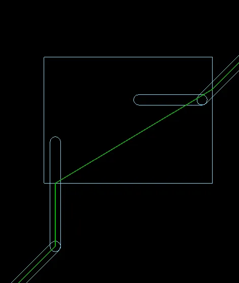
Одна из сложностей стратегии трассировки Balanced T — как выровнять длину магистралей и ветвей за T-точками. Доступные узлы в цепи есть только на площадках, поэтому невозможно определить отдельные xSignals для магистрали и для участка от точки ветвления до конца каждой ветви. Точки ветвления обозначены красными точками на изображении ниже.
Один из способов решить эту проблему — добавить в цепь компонент с одним выводом. Создайте компонент с одной площадкой, размер которой соответствует используемым в проекте переходным отверстиям. Если площадка компонента точки ветвления однослойная, то ее также можно использовать в сочетании со слепым или скрытым переходным отверстием, разместив ее на стартовом или конечном слое via, что дает полную гибкость в том, как будет выполнена трассировка. Если вы хотите включить компонент точки ветвления только на PCB, установите для него Type в Mechanical, чтобы исключить его из BOM и предотвратить проблемы синхронизации со схемой. Если вы планируете включить компонент точки ветвления на схему, параметр компонента Type можно установить в Standard (no BOM).

Трассировка Balanced T может требовать согласования длин между промежуточными точками ветвления.
Поскольку точка ветвления является узлом в цепи, теперь можно определить xSignals только для магистрали, для каждой основной ветви и, при необходимости, для каждой вторичной ветви. Затем их можно использовать для ограничения области действия правил согласования длины, предоставляя проектировщику полный контроль над тем, насколько детально выполнять согласование длин.
Управление xSignals
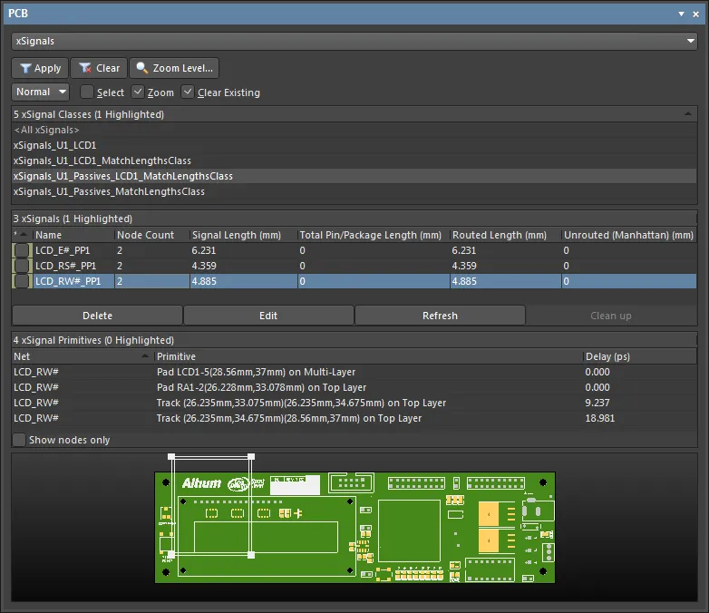
В режиме панели PCB xSignals ее три основные области изменяются, чтобы отражать иерархию xSignal текущего проекта PCB (сверху вниз):
- xSignal Classes
- Отдельные xSignals внутри класса
- Отдельные xSignal Primitives, составляющие xSignal (площадки, дорожки и переходные отверстия)
Область классов xSignal
Область xSignal Classes содержит список коллекций классов xSignal, которые были определены, или всех доступных классов (<All xSignals>).
Выберите класс, чтобы увидеть список его xSignals в средней области (xSignals) и отобразить их в рабочем пространстве PCB.
Чтобы создать новый класс xSignal из существующей коллекции xSignal, щелкните правой кнопкой мыши в этой области и выберите Add Class в контекстном меню, чтобы открыть диалог Edit xSignal Class dialog. В диалоге перечислены доступные xSignals, которые можно добавлять или удалять как элементы нового класса с помощью кнопок управления. Используйте поле Name, чтобы задать подходящее имя для нового класса xSignal.

Создавайте класс xSignal или добавляйте в него, добавляя/удаляя элементы xSignal с помощью диалога Edit xSignal Class.
Контекстное меню (по правому клику) этой области панели также позволяет удалить (Delete) или изменить визуальное представление в рабочем пространстве PCB (например, Change xSignal Color).
Область xSignals
Средняя область панели отображает xSignals из класса(ов) xSignal, выбранных в области выше.
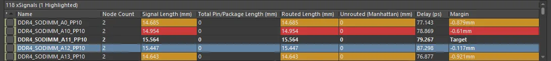
По умолчанию для каждого xSignal отображается следующая информация:
-
 – у этой функции две задачи:
- цвет фона – цвет, назначенный xSignal (тонкая линия, представляющая xSignal в рабочем пространстве). Щелкните правой кнопкой мыши, чтобы Change xSignal Color для всех выбранных в данный момент xSignals.
- флажок видимости – используйте его, чтобы всегда отображать xSignal независимо от того, выбран он сейчас или нет.
- Name – имя xSignal.
- Node Count – общее количество площадок в этом xSignal.
- Routed Length – сумма длин размещенных сегментов дорожек и дуг, формирующих трассировку, плюс вертикальное расстояние, пройденное через переходные отверстия (см. примечание ниже). Калькулятор длины трассировки не пытается разрешать перекрывающиеся сегменты дорожек или «змейки» внутри площадок.
- Signal Length – точный расчет полного расстояния от узла к узлу. Для расчетов Signal Length применимы следующие примечания:
- Total Pin/Package Length – сумма всех значений Pin Package Length во всех площадках данного xSignal. Это значение задается как свойство площадки PCB и также может быть указано в выводе на схеме.
- Unrouted (Manhattan) Length – вертикальное плюс горизонтальное (X+Y) расстояние всех нетрассированных участков.
- Margin – разница между фактической длиной сигнала и целевой длиной, заданной применимыми правилами Length/Matched Length.
Щелкните правой кнопкой мыши в области и используйте подменю Columns, чтобы добавить следующий столбец:
- Delay – время, за которое сигнал распространяется по этому маршруту.
Используйте подменю Columns, чтобы показывать/скрывать столбцы.
Vertical distance through a via – вертикальное расстояние, которое сигнал проходит через via, равно сумме толщин всех слоев (медь и диэлектрик) между медными слоями start и stop, плюс половина толщины стартового слоя и половина толщины конечного слоя. Толщины слоев задаются в
Layer Stack.
Область примитивов xSignal
Третья область панели PCB, xSignal Primitives, перечисляет все составляющие элементы (примитивы) текущего выбранного xSignal.
Установите флажок Show nodes only в этой области, чтобы ограничить список примитивов площадками, которые являются узлами начальной/конечной точки xSignal. В этом режиме выбранный xSignal будет показан в рабочем пространстве PCB как узловые площадки, соединенные тонкой линией (а не дорожками), представляющей путь xSignal.

Нижняя область xSignal Primitives перечисляет все элементы выбранного xSignal, такие как площадки, переходные отверстия и дорожки, а также соответствующую им задержку.
Отображение xSignals в рабочем пространстве
xSignals отображаются в рабочем пространстве тонкой линией. Линия показывает путь, по которому проходит xSignal. Общая длина линии — это вклад X/Y в длину сигнала данного xSignal. Вклад Z, или вертикальная составляющая общей длины сигнала, описан выше.
На изображении ниже показаны xSignals для дифференциальной пары. xSignal для невыбранного участника пары остается видимым, потому что для этого xSignal в панели включен флажок.

xSignals представлены в рабочем пространстве тонкой линией. Оба xSignals в этой дифференциальной паре остаются видимыми, хотя в панели выбран только один, поскольку включен флажок видимости.
Удаление xSignal
Выберите xSignal в панели, затем нажмите кнопку Delete под списком xSignals. Либо щелкните правой кнопкой мыши и выберите Delete в контекстном меню, либо нажмите Delete на клавиатуре.
Ключевые слова запросов xSignal
Редактор PCB включает мощный и продвинутый filtering engine. Этот механизм используется для идентификации объектов при поиске объектов в рабочем пространстве, применении правил во время интерактивных и автоматических задач проектирования, а также для проверки соблюдения правил. Проектировщик сообщает механизму фильтрации, какие объекты его интересуют, записывая запрос с использованием ключевых слов, распознаваемых механизмом фильтрации.
Для использования в правилах проектирования и фильтрах рабочего пространства добавлены следующие ключевые слова запросов типа xSignal:
Ключевые слова типа проверки принадлежности
- InxSignal - Находится ли объект в указанном xSignal, например,
InxSignal('DRAM_A0_PP1')
- InxSignalClass - Находится ли объект в указанном классе xSignal, например,
InxSignalClass('PCIE')
- IsxSignal - Является ли объект xSignal с указанным именем, например,
IsxSignal('DRAM_A0_PP1')
Ключевые слова типа проверки атрибутов
- InAnyxSignal - Находится ли объект в каком-либо xSignal, например,
InAnyxSignal
Поддержка xSignals в правилах проектирования
Правила проектирования — это способ перевести ваши требования в набор инструкций, которые редактор PCB может понимать и выполнять. Правила могут проверяться во время размещения объектов (Online DRC) или как постобработка (Batch DRC). xSignals можно использовать для определения объектов, к которым должно применяться правило проектирования.
► Узнать больше о Design Rules
► Узнать больше о Length Tuning
Правило Matched Length
Правило проектирования Matched Length используется для того, чтобы гарантировать, что длина указанных цепей (nets) находится в заданном диапазоне. Это правило критически важно в высокоскоростных проектах, где задача заключается не только в том, сколько времени требуется сигналам, чтобы прийти (что определяется их общей длиной), но и в том, насколько важно, чтобы заданные сигналы приходили одновременно. В зависимости от скоростей переключения сигналов, назначения сигнала и материалов, используемых в плате, допустимая разница может составлять как 500 mil, так и всего 1 mil.
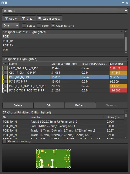
На изображении ниже показан пример правила Matched Length, настроенного на xSignals в классе xSignal PCIE, и проверяющего разницу длин внутри каждой дифференциальной пары в этом классе xSignals. Каждая пара в классе должна иметь трассированные длины, которые дают Delay Tolerance не более 2ps задержки между двумя цепями в этой паре.
 правила Matched Length требуется выбрать между выравниванием длины всех целевых цепей (Group Matched Lengths) и выравниванием двух цепей внутри каждой дифференциальной пары среди целевых цепей.")
Обратите внимание: в ограничениях (Constraints) правила Matched Length требуется выбрать между выравниванием длины всех целевых цепей (Group Matched Lengths) и выравниванием двух цепей внутри каждой дифференциальной пары среди целевых цепей.
На изображении ниже показан выбранный в панели класс xSignal PCIE_TX и соответствующие xSignals, выделенные в рабочем поле.

Помимо класса PCIE, также определены классы для пар TX и RX. Обратите внимание, что один из xSignals TX не проходит применимое правило согласования длины. ##
Если вы планируете выполнять подстройку длины (length tuning) для xSignals, которые включают одиночные цепи и дифференциальные пары, создайте следующие правила:
- Правило matched length, которое задаёт требования к согласованию длины between nets and differential pairs in xSignals. Чтобы настроить правило на проверку длины одной цепи/пары относительно длины другой цепи/пары, включите опцию Group Matched Lengths .
- Второе правило matched length с более высоким приоритетом, которое задаёт within-pair требования к согласованию длины. Чтобы настроить правило на проверку длины одного проводника пары относительно другого проводника пары, включите опцию Within Differential Pair Length .
Хороший подход к подстройке длин таких xSignals:
- Проложите (route) цепи и дифференциальные пары xSignal.
- Выполните подстройку длины одиночных цепей командой Interactive Length Tuning .
- Выполните подстройку длины between пар командой Interactive Differential Pair Length Tuning . При подстройке длины в качестве Target Length используется самая большая длина сигнала в самой длинной паре, и самая длинная цепь в паре подгоняется до этой длины.
- Выполните подстройку длины более короткой цепи within в каждой паре относительно другой цепи в паре командой Interactive Length Tuning .
- Теперь можно использовать панель PCB Rules and Violations для проверки правила(ил) within-pair Matched Net Length. Для этого выберите Matched Net Lengths в разделе Rule Classes панели, затем щёлкните правой кнопкой по нужному правилу Matched Length и выберите команду Run DRC Rule <RuleName> в контекстном меню. При необходимости скорректируйте «гармошки» (accordions) подстройки для одиночных цепей.
- Затем используйте панель PCB Rules and Violations для проверки правила(ил) between-pair Matched Net Length, применяя только что описанный процесс. При необходимости скорректируйте «гармошки» подстройки для дифференциальных пар.
Правило Length
Правило проектирования Length используется для того, чтобы гарантировать, что общая трассированная длина находится в заданном диапазоне. Обычно это правило применяют, чтобы убедиться, что целевые цепи не длиннее заданного значения — например, чтобы обеспечить выполнение требований по таймингу схемы. Правило Length учитывает запросы (queries) по типам xSignal, перечисленные выше.
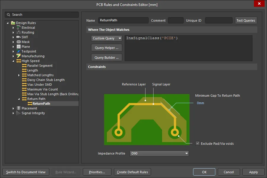
Правило Return Path
Правило проектирования Return Path проверяет наличие непрерывного пути возврата сигнала на назначенном опорном слое (reference layer) над или под сигналами, на которые нацелено правило. Путь возврата может быть сформирован заливками (fills), областями (regions) и полигональными заливками (polygon pours), размещёнными на сигнальном слое, либо это может быть слой плоскости (plane layer).
Слои пути возврата — это опорные слои, определённые в выбранном профиле импеданса (Impedance Profile). Добавьте новое правило проектирования Return Path в категории правил High Speed.
На изображении ниже показано нарушение правила Return Path: в полигоне пути возврата xSignal есть отверстие, через которое проходит переходное отверстие (via).
 Использование панели PCB Rules and Violations для поиска нарушения правила Return Path. ##
Точные расчёты длины
Ключевое требование при задании правил для высокоскоростного проектирования — точный расчёт длин трасс. Традиционный подход к вычислению длины сигнала — суммировать длину по осевой линии (centerline) всех сегментов, используемых в трассе, а также вертикальную составляющую из‑за высоты переходных отверстий, которая изначально определялась толщиной платы.
Этот подход недостаточен для высокоскоростного проектирования по ряду причин, включая:
- Сложенные и перекрывающиеся объекты — алгоритм, который просто суммирует длину по осевой линии всех объектов в цепи, не учитывает сложенные или перекрывающиеся объекты.
- «Блуждающий» путь трассы внутри объекта — часто встречаются объекты трассировки, полностью находящиеся внутри площадки (pad) или via, что может ошибочно добавлять длину, как показано на первом изображении ниже. Второе изображение показывает корректный способ расчёта длины, когда объект заливки является частью трассировки.
- Длина via — глухие и скрытые переходные отверстия (blind и buried vias) не проходят через все слои платы, поэтому толщины платы недостаточно для точного определения вертикальной длины. Нужно использовать фактическую высоту via, учитывая толщины меди и диэлектрика, через которые проходит via.
Калькулятор длины в PCB‑редакторе возвращает максимально точную возможную длину трассы.

Расчёт длины выполняется точно по осевой линии кратчайшего пути, как показано на этих двух изображениях.

Для via рассчитываются точные длины на основе пройденных слоёв и размеров стека. Изображение из панели PCB в режиме Nets.
Задержка вывода в корпусе (Pin Package Delay)
В каждом высокоскоростном проекте свыше 500 МГц среда соединения — или бонд‑провод к кристаллу — вносит задержку в сигнал. Эта внутриприборная задержка называется задержкой вывода в корпусе (pin‑package delay). Даже если два устройства полностью совместимы по выводам с точки зрения схемы и PCB, времена пролёта (package flight times) будут различаться у разных устройств, поэтому их нужно учитывать. Информацию о времени пролёта можно найти в документе IBIS 6 для устройства. Данные по выводам корпуса (Package Pins) следует учитывать на этапе планирования I/O или после синтеза для FPGA. Все производители должны иметь возможность предоставить задержки корпуса, которые будут указаны либо как задержка в пикосекундах, либо как эквивалентная длина.
Задержку можно включить в проект либо как Pin Package Length, либо как Propagation Delay, используя соответствующие поля для вывода в редакторе схем или для pad/via в PCB‑редакторе. Введённые значения обрабатываются следующим образом:
Pin Package Length - все длины pin package в пределах каждой цепи суммируются в PCB‑редакторе, формируя Total Pin/Package Length, который включается в общий Signal Length для этой цепи. См. режим Nets панели PCB, чтобы узнать больше о Signal Length.
Propagation Delay - все пользовательские значения задержки, заданные для выводов/площадок и via в каждой цепи, добавляются к задержке трассировки (routing delay) для этой цепи в PCB‑редакторе. Задержка трассировки автоматически рассчитывается полевым решателем Simbeor® (field solver), встроенным в Layer Stack Manager. Задержки pad и via автоматически не рассчитываются, но могут быть заданы пользователем.
- Правила Length и Matched Length можно настраивать на основе Length или Delay.
- Signal Length, Total Pin/Package Length и Delay могут отображаться в различных режимах панели PCB, включая режим Nets mode, Differential Pairs Editor mode и xSignals mode. Щёлкните правой кнопкой по заголовку столбца в панели PCB, чтобы включить/отключить столбцы.
- Simbeor SFS (квазистатический полевой решатель) от Simberian® используется для расчёта задержки трассировки на основе физических свойств, заданных в Layer Stack Manager.
- Пользовательские значения Pin Package Length и Propagation Delay независимы друг от друга; они добавляются к значениям Signal Length и Delay, как описано выше. Поскольку они не взаимодействуют друг с другом, при необходимости можно задавать оба значения.
Включение задержки в схему
Длины pin package можно задать как атрибут вывода компонента на схеме в панели Properties в режиме Pin. По умолчанию ПО использует единицы измерения базового документа; при необходимости укажите единицы вместе со значением.

Введите длину pin‑package с требуемыми единицами измерения.
- Свойства выводов компонента также можно редактировать в редакторе библиотек или на листе схемы на вкладке Pins панели Properties в режиме Component. Нажмите
 на этой вкладке панели, чтобы открыть Component Pin Editor, где можно редактировать все свойства всех выводов данного компонента. Значения можно изменять прямо в таблице (выберите ячейку и введите новое значение), а клавиши курсора можно использовать для перехода к соседним ячейкам. Единицы по умолчанию будут автоматически добавлены, если их не ввести вручную.
- В качестве альтернативы используйте панель SCH List panel, чтобы копировать/вставлять несколько значений Pin/Pkg Lengths или Propagation Delay из даташита в набор выбранных выводов компонентов в редакторе библиотек схем (show image
![]() ). Помимо вставки содержимого буфера обмена напрямую в выбранные ячейки, вы также можете щёлкнуть правой кнопкой мыши в панели, чтобы открыть диалог Smart Grid Paste dialog, который даёт больше контроля над процессом добавления дополнительных данных в выводы.
). Помимо вставки содержимого буфера обмена напрямую в выбранные ячейки, вы также можете щёлкнуть правой кнопкой мыши в панели, чтобы открыть диалог Smart Grid Paste dialog, который даёт больше контроля над процессом добавления дополнительных данных в выводы.
Определение задержки в редакторе PCB
Значения Pin Package Length и Propagation Delay переносятся в разводку PCB, как видно в режиме Pad панели Properties.

Значения Pin Package Length и Propagation Delay переносятся со схемы в PCB, либо их также можно задать непосредственно в PCB.
Проверка Pin/Package Length и Propagation Delay в панели PCB
Значение Pin/Pkg Length автоматически включается в расчёты Signal Length, которые отображаются в различных режимах панели PCB. Установите панель в режим Nets, чтобы просмотреть (или отредактировать) значение Pin/Pkg Length для выводов в выбранной цепи (net). Обратите внимание, что столбец Routed Length отражает длину трассировки, а столбец Signal Length отражает длину трассировки плюс любые значения Pin/Pkg Length в этой цепи.

Значение Pin/Pkg Length и его влияние на Signal Length показано в режиме Nets панели PCB.
На изображении ниже в столбце propagation Delay видно, что есть две пары xSignals, которые не проходят правило проектирования Matched Length. Поскольку подсветка находится в столбце Delay, это указывает на то, что правило настроено на использование единиц задержки (Delay Units), а не единиц длины (Length Units).
 Столбец Delay показывает, что есть две пары xSignals, которые не проходят правило проектирования Matched Length.
Signal Length, Total Pin/Package Length и Delay могут отображаться в различных режимах панели PCB, включая режим Nets mode, режим Differential Pairs Editor mode и режим xSignals mode. Щёлкните правой кнопкой мыши по заголовку столбца в панели PCB, чтобы включать/отключать столбцы.
Как длина учитывается в xSignals
Значение Pin/Pkg Length автоматически включается в общую длину xSignal, когда:
-
Этот сигнал является частью определения xSignal
-
Этот пад не подключён по схеме трассировки fly-by (к этому паду подключена только одна дорожка)
Пады, подключённые по схеме трассировки fly-by (с точкой входа и точкой выхода), исключаются из расчёта длины.
Терминология, связанная с цепями (net)
В редакторе PCB используется следующая терминология:
- Net
– набор выводов компонентов (узлов), соединённых друг с другом. Способ соединения этих узлов называется топологией; топология по умолчанию — shortest.
- From-To
– концептуально From-To проходит между двумя узлами в цепи (net). From-To можно создавать так, чтобы они следовали топологии или расположению узлов в этой цепи. Например, топология цепи может быть от R1-1 к U1-5 к U3-2 к R5-2. Для этой цепи может быть три From-To: R1-1 → U1-5; U1-5 → U3-2; и U3-2 → R5-2. Если топология изменится, изменятся и возможные From-To. From-To создаются в режиме From-To панели PCB либо нажатием кнопки Generate для создания на основе топологии, либо выбором двух падов в цепи и последующим нажатием кнопки Add From To.
- xSignal
– определяемый пользователем набор узлов, обычно подмножество цепи (от этого узла к тому узлу) или комбинация двух цепей, включающая последовательный компонент, например терминальный резистор.

 Локализовано с помощью ИИ