Working with Tracks
A Track segment is a straight line of a defined width. Use tracks to define a straight line in the PCB design space. Tracks are placed on a signal layer to form the electrical interconnections, or routing, between component pads. Tracks placed on a non-electrical layer are called Lines, where they are used as general-purpose drawing elements to create component outlines, instructional information, keepout boundaries, etc. Tracks also are used in group design objects, such as dimensions and coordinates.

Track objects are used for routing and for general-purpose drawing lines. There are four placed track segments in the image above, and another in the process of being placed.
Although tracks and lines are actually the same object, the difference is how the software behaves during their placement, which is why there are different commands. When a track placement command is run, such as Interactive Routing, the software monitors the click location and automatically adopts the net name of an existing object (such as a pad) under the click location. It also monitors and obeys any applicable design rules. When a line placement command is run (Place » Line), these monitoring behaviors do not occur.
Tracks are available for placement in both PCB editor and the PCB Library editor. Regardless of which command is used (routing/track or line placement), the basic placement behavior is the same. After launching the command, the cursor will change to a crosshair and you will enter track placement mode. Placement is made by performing the following sequence of actions:
-
Click or press Enter to anchor the starting point for the first track segment. If a routing-type placement command is being run and you click to start placement on an existing object, the track will adopt the net name of that object. For routing, the width will be determined by the applicable Routing Width design rule; this can be overridden by certain interactive routing options, which are described in more detail below.
-
Move the cursor to define the track segment then click or press Enter to anchor the end point for this first segment, which is also the starting point for the next connected segment.
-
Continue to position the cursor then click or press Enter to anchor a series of vertex points that define the series of connected track segments.
-
Right-click or press Esc to end the current series of connected track segments.
Additional actions that can be performed during placement include:
-
Press the * key on the numeric keypad to cycle through the available signal layers. Alternatively, use the Shift+Ctrl+Wheel Roll combination to move through the routing layers; each notch of the mouse wheel will move to the next (or previous) available signal layer.
-
Press the + and - keys on the numeric keypad to cycle forward and backward through all layers currently visible in the design.
While placing track segments there are five available corner modes, four of which also have corner direction sub-modes. During placement:
-
Press Shift+Spacebar to cycle through the available corner modes.
-
Press Spacebar to toggle between the two corner direction sub-modes.
-
When in either of the arc corner modes, hold the , or . key to shrink or grow the arc. Hold the Shift key as you press to accelerate arc resizing.
-
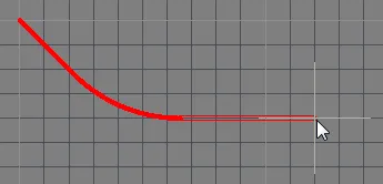
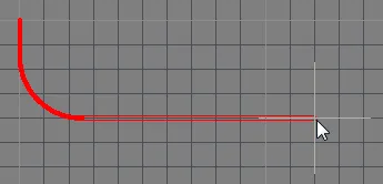
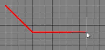
Press the 1 shortcut key to toggle between placing one segment per click (shown in the first five images below), or two segments per click (shown in the last image below). In the first mode, the hollow track segment is referred to as the look-ahead segment.
-
Press the Backspace key to remove the last vertex.


Press Shift+Spacebar to cycle through the five available corner modes, press Spacebar to toggle the corner direction, press the 1 shortcut to toggle placement between one segment or two segments.
The graphical method of editing allows you to select a placed track object directly in the design space and change its size, shape or location graphically.
When a track object is selected, the following editing handles are available:

A selected Track
-
Click and drag A to reposition the end points of the track.
-
Click and drag B to change the shape of the track.
The PCB editor includes sophisticated algorithms for moving track segments on the board so that the arrangement of the routing can be maintained. This sliding of track segments can be invoked interactively either by clicking to first select the track segment and then clicking and holding when the special cursor appears to slide the segment or by clicking and holding on a track segment and sliding it. Sliding behavior can be configured using the Dragging options on the PCB Editor - Interactive Routing page of the Preferences dialog. These options allow you to assign the Move action to a track, which is useful if you want to be able to freely move an individual track segment.

Control track sliding behavior with dragging options set at the Preferences level.
If the Move action is assigned through these options, the track segment can be rotated or mirrored during the move.
Interactive Routing and the Applicable Design Rules
During Interactive Routing, the default behavior is for the software to ensure the track segments are placed in accordance with the applicable Electrical and Routing design rules. That means the software will not allow a new track segment to be placed that violates an existing track segment that belongs to a different net; instead, it will clip the track segment to meet the design rules. This interactive routing behavior is known as the Routing Conflict Resolution mode. The default mode is Stop at First Obstacle (the current mode is displayed on the Status bar). Press Shift+R to cycle through the available modes.
The term applicable design rules means all the rules that apply to the object being placed. The design rules engine works on a system where you scope exactly to which objects you want each rule to apply. During placement, the design rules engine is queried to determine the highest priority rule that applies in the current placement situation. Rules that apply during Interactive Routing include:
-
Electrical Clearance
-
Routing Width
-
Routing Via Style
The animation below demonstrates routing in action. The net GND is being routed in accordance with a defined and applicable Routing Width design rule. Note that when the cursor is moved over the via associated to the +12V net, the route is automatically being clipped to ensure the applicable Electrical Clearance Constraint design rule is being met.

The applicable routing width and clearance design rules are automatically obeyed during interactive routing.
How the Routing Width is Determined
Unless the rules engine is disabled, the overriding behavior of the software is to always ensure that the routing width is within the range allowed by the applicable Routing Width design rule. A common approach is to allow a range of widths to be used for a net to give you flexibility in fitting in the route while satisfying the current carrying requirements of that net. Supporting this, the Routing Width design rule has Min, Preferred and Max settings in the PCB Rules and Constraints Editor that can be configured to allow a range of widths or can be set the same to require a specific width. The width can also be configured as an Impedance and can also have a different range specified for each signal layer.

The default Routing Width design rule is applied to all nets for a new PCB.
As the designer, you have a number of options that can help select the most appropriate routing width when you begin routing. These are configured on the PCB Editor — Interactive Routing page of the Preferences dialog, as shown below.

The Interactive Routing Width Sources options determine what size is used when you start a route.
Note the Track Width Mode is set to Rule Preferred in the image. This denotes that when the route commences on an existing net object, such as a pad, this is the width that will be used. However, if the route commences on an existing track, then the Pickup Track Width From Existing Routes option will override the Track Width Mode and set the new width to match the existing width.
As the designer, you can also press the Shift+W shortcut while routing to access a dialog where a different width can be selected, or you can press Tab to open the Properties panel and type in a new Width value. The value chosen or entered must lie between the Min and Max settings defined in the applicable rule. If not, it is automatically clipped back to the nearest of these.
Interactive Routing Shortcuts
While you are routing, there are a number of shortcuts that are available. For example, you can press Shift+R to cycle through the available conflict resolution modes, or press Backspace to delete the last placed vertex (corner). To display a list of shortcuts while you are routing, press Shift+F1. A menu of available interactive shortcuts is displayed; select the required shortcut or press Esc to close the menu and use the shortcut key sequence.

During interactive routing, press Shift+F1 to display a menu of available interactive shortcuts
Moving a Track
The Edit » Move sub-menu and the movement command menu in the Active Bar includes a number of commands that can be used to change the position or the shape of a track.

Re-Route
This command enables you to manually reroute existing track on the board. After launching the command, the cursor will change to a cross-hair and you will be prompted to choose a track. Position the cursor over the required track then click or press Enter. The functionality of this feature depends on whether or not the Preserve Angle When Dragging option is enabled on the PCB Editor - Interactive Routing page of the Preferences dialog:
-
Preserve Angle Dragging enabled - the track will be broken with a new segment added to maintain the orthogonal/diagonal connections. Move the cursor to slide this segment as required then click to effect placement. Right-click or press Esc at this point otherwise that new segment will be broken with a further segment. Use the Shift+R keyboard shortcut to cycle through options that control how obstacles should be handled during dragging (Ignore Obstacles, Avoid Obstacles, or Avoid Obstacles (Snap Grid)). If one of the Avoid Obstacles modes is enabled, the rules will be obeyed during dragging preventing you from dragging a segment into violation.
-
Preserve Angle Dragging disabled - both ends of the track segment will be anchored and you can now lay new segments of track between the two. Click or press Enter to place a new segment of track. Continue placing new track segments for the reroute or right-click or press Esc to stop.
Continue rerouting further tracks or right-click or press Esc to exit.
-
If Preserve Angle Dragging is enabled, you can effectively disable it temporarily by holding the Alt key before clicking on the target track segment. Continue to hold the Alt key while progressively clicking to reroute.
-
When rerouting track using this command and with Preserve Angle Dragging disabled, it is advisable to start the reroute from the left end of the chosen track segment and work towards the right end.
-
Similar re-routing functionality can be achieved by selecting a track segment then clicking-and-dragging its center vertex. Then subsequent clicking-and-dragging on resulting segment's center vertices along the original track from one end to the other.
Break Track
This command enables you to create a vertex (or break) in a track segment. After launching the command, the cursor will change to a crosshair and you will be prompted to select a track. Position the cursor over the required track segment at the specific point along the segment where you want to insert a break then click or press Enter. A vertex is inserted, effectively breaking the original segment into two.
Move the vertex to the required position then click or press Enter to place. The attached track segments behave according to the setting of the Preserve Angle When Dragging option on the PCB Editor - Interactive Routing page of the Preferences dialog:
-
Preserve Angle When Dragging enabled - the angles to adjacent track segments are preserved, maintaining the routing style.
-
Preserve Angle When Dragging disabled - the two individual track segments will rubber band to accommodate the move without maintaining the existing routing style.
Continue breaking more track segment or right-click or press Esc to exit.
You also can break a track segment at the current cursor position by using the Shift+Ctrl+Click&Hold keyboard shortcut.
Drag Track End
This command enables you to manually reposition or drag the end of a routed track segment. After launching the command, the cursor will change to a cross-hair and you will be prompted to select an object. Position the cursor over a track then click or press Enter. The cursor will jump to the end of the track segment that it is nearest to and the track end will be attached to the cursor. Move the end of the track to the desired position then click or press Enter to effect placement.
-
If the end of the chosen track segment is a vertex point to which no other track segments are connected, move the vertex to the required position.
-
If the end of the chosen track segment is a vertex point to which two track segments are connected, the attached track segments will rubber-band as the vertex is moved.
-
If the end of the track segment is connected to a component pad, moving the end will disassociate it from the pad. After the end is repositioned, a logical connection line will be shown from the track end to the pad provided the Smart Track Ends option is enabled on the PCB Editor – General page of the Preferences dialog.
-
If the end of the track segment is connected to a free pad, the pad will become attached to the cursor ready for repositioning. All track connected to the pad will rubber-band accordingly.
-
If the end of the track segment is connected to a via, the via will become attached to the cursor ready for repositioning. All track connected to the via will rubber-band accordingly.
Continue dragging further track ends or right-click or press Esc to exit.
-
This command is overridden if the Preserve Angle When Dragging option is enabled on the PCB Editor - Interactive Routing page of the Preferences dialog.
-
This feature also can be invoked by selecting the required track first then clicking and dragging the required end vertex.
Move / Resize Tracks
This command is used to move the end-points of multiple selected track segments, effectively resizing the segments. After launching the command, the cursor will change to a cross-hair and you will be prompted to choose a track end-point. To move/resize the tracks:
-
Position the cursor on the end-point of one of the segments in the selection then click or press Enter.
-
Move the cursor; all of the track segments in the selection will resize dynamically while maintaining original distances and angles between each other. The other end of each segment will rubber-band to maintain its existing connection/location.
-
Once the segments are in the desired location, click or press Enter to effect placement and exit movement mode.
-
To cancel out of the operation, right-click or press Esc.
While moving the segments around, the following additional controls are available:
-
Press the Tab key to cycle the cursor between the end-point of each track segment in the selection.
-
Hold the Alt key while moving to constrain movement in a particular direction dependent on initial direction moved. Horizontal, vertical and 45 degree angle directions are possible.
-
Press the Spacebar twice to quickly make all end-points of the track segments in-line with each other in either the horizontal or vertical planes. Press the Spacebar twice quickly again to return to the previous sizing.
This command also can be used to move the end-point of a single, un-selected track segment. Note that only the Alt key additional control can be used in this case.
Slicing Tracks
The Track Slicer tool provides an easy mechanism for cutting one or more track segments into two and can slice tracks on the current signal layer or all visible signal layers. To access the tool, choose the Edit » Slice Tracks command from the main menus.
After launching the command, the cursor will change to a cross-hair and you will be prompted to choose a starting location for the slice. In addition, filtering is applied to only show track objects within the workspace. This will either be all track across all visible signals layers or only track on the current signal layer, depending on the active setup of the Track Slicer. To slice one or more tracks:
-
Position the cursor then click or press Enter to anchor the starting point for the slice.
-
Move the cursor across the point of the track, or tracks, where you want to slice - the path of the slicer is shown by a line with the prospective cut(s) visually depicted.
-
Click or press Enter to anchor the end point of the slicer's track.
-
Continue slicing further track segments, or right-click or press Esc to exit slice mode.
Additional actions that can be performed - after the initial anchor point for the slice has been chosen, and while moving the 'slicing line' - are:
-
Press the B key to cycle between cutting track on the current signal layer only, or track on all visible signal layers.
-
Press the Spacebar to switch the cutting angle between 45 Degree increments or Any Angle.
-
Press the N key to cycle the slicer blade side between Left, Right and Middle.
-
Press the / key to select all sliced tracks.
-
Press the "," key to select sliced tracks to the left of the slicer.
-
Press the "." key to select sliced tracks to the right of the slicer.
-
Press the M key to not have any sliced tracks selected.
-
Press the Tab key to access the Slicer Properties dialog, from where properties for the Track Slicer can be changed on-the-fly.

The Slicer Properties dialog
-
A track segment is sliced such that the extents of the blade pass through what will become the centers of the hotspots of the resulting two segment ends.
-
You can freely define the width of the slicing blade through the Slicer Properties dialog. Alternatively, you can constrain the width of the blade based on the current Snap grid. If the value for the Blade Width is not a multiple of the Snap grid, it will be clipped so that it is on-grid. The resulting width is known as the Gridded Width. If this option is disabled AND the Blade Width is not a multiple of the current Snap grid, one or both of the resulting track segment ends may reside off-grid. If the Blade Side is set to Left or Right, the track end at the extent of the blade will be located off-grid (the track end along the starting location axis will remain on-grid). If the Blade Side is set to Both, then both track ends will reside off-grid.
-
The Blade Side option controls how the slice is made, in relation to the axis determined from the chosen starting location for the slice. In the design space, the axis determined by the chosen starting location appears as a solid line, while the extent of the blade appears as a dashed line. The following options are available:
-
Left - the slice will be made to the left of the starting location axis. The slice distance will be equal to the full Blade Width, or Gridded Width, as applicable.
-
Right - the slice will be made to the right of the starting location axis. The slice distance will be equal to the full Blade Width, or Gridded Width, as applicable.
-
Both - the slice will be made equally to the left and right of the starting location axis. The slice distance on each side will be equal to half the full Blade Width, or half the Gridded Width, as applicable.
-
Enable the Cut Current Layer Only option to only slice through track segments on the current layer only. Disable this option to slice through track segments on all visible layers, where those segments fall within the 'path' of the Track Slicer.
-
The extent of masking when filtering is applied to the workspace can be manually adjusted using the Dimmed Objects slider bar located in the Mask and Dim Settings section on the View Options tab of the View Configuration panel. Clear filtering by using the Shift+C keyboard shortcut.
Converting Tracks to Chamfered Path
The chamfering of 90 degree routing corners is a technique used to reduce reflections caused by the corner in a microwave frequency route. Arcs can be used but should have a radius of at least 3x the route width. Chamfering (also called mitering) is an alternative where the outer point of the corner is sliced off. Because Altium Designer's track objects have rounded ends, they cannot be used to create a chamfered corner. To create the chamfered corner, the selected track segments are replaced with region objects.
Select all the track segments to be chamfered and then select the Tools » Convert » Convert Selected Tracks to Chamfered Path command from the main menus. The Convert Tracks to Chamfered Path dialog will open. Use this dialog to configure the chamfer then click OK. Each selected track segment pair (with offending 90 degree angles) will be replaced with chamfered cornering and the original track segments in each pairing will be converted to a single solid (copper) region object.

Selected tracks will be chamfered by the specified amount at each right-angle corner.
Use the following options in the dialog to configure the chamfer:
-
Chamfer - amount of the outside corner that is to be sliced off, or chamfered, as a percentage of the existing diagonal corner distance.
-
Inside Chamfer - amount of material to be added to the inside corner as a percentage of the existing diagonal corner distance.
How big should the Chamfer be?
The percentage mitre is the cut-away fraction of the diagonal between the inner and outer corners of the un-mitred bend.

The optimum mitre for a wide range of microstrip geometries has been determined experimentally by Douville and James. They find that a good fit for the optimum percentage mitre is given by

Subject to  and with the substrate dielectric constant
  .
.
This formula is entirely independent of  . The actual range of parameters for which Douville and James present evidence is
  and
and  . They report a VSWR of better than 1.1 (i.e. a return better than −26 dB) for any percentage mitre within 4% (of the original
  ) of that given by the formula. At the minimum
  of 0.25, the percentage mitre is 98.4%, so that the strip is very nearly cut through.
The process of chamfering converts multiple track segments into a single region object. This is a one-way process; once the tracks have been converted to a region, they cannot be converted back. For this reason chamfering should only be performed once all routing is complete. If you are unsure, save off a copy of the board before chamfering.
Track Properties

The Track mode of the Properties panel.
Net Information
This region provides information about the net that the track belongs to, as well as the differential pair and/or xSignal if that net is a member. Class information is shown where appropriate. Delay, Length, Max Current, and Resistance values are also provided.
Refer to the PCB Placement & Editing Techniques page to learn more about net information.
Location
The

icon to the right of this region must be displayed as

(unlocked) in order to access the below fields. Toggle the lock/unlock icon to change its lock status.
-
(X/Y)
-
X (first field) – the current X (horizontal) coordinate of the reference point of the track relative to the current design space origin. Edit to change the X position of the track. The value can be entered in either metric or imperial; include the units when entering a value whose units are not the current default.
-
Y (second field) – the current Y (vertical) coordinate of the reference point of the track relative to the current origin. Edit to change the Y position of the track. The value can be entered in either metric or imperial; include the units when entering a value whose units are not the current default.
Properties
-
Component – this field is shown in the PCB editor only when the selected Track is a constituent part of a PCB Component and displays the designator of the parent PCB component. Select the clickable Component link to open the Component mode of the Properties panel for the parent component.
-
Net – use to choose a net for the track. All nets for the active board design will be listed in the drop-down list. Note that if object placement commences at the same location as an existing object that is already connected to a net, then the Net property of the new object is automatically assigned to that net. Select No Net to specify that the track is not connected to any net. The Net property of a primitive is used by the Design Rule Checker to determine if a PCB object is legally placed. Alternatively, you can click on the Assign Net icon (
 ) to choose an object in the design space - the net of that object will be assigned to selected track(s).
-
Layer – use the drop-down to select the layer on which the track is located.
-
Width – displays the current width of the track. Edit this field to change the track width within the range 0.001mil to 10000mil.
-
Start (X/Y) – displays the current X/Y coordinate of the track start point relative to the current origin.
-
End (X/Y) – displays the current X/Y coordinate of the track end point relative to the current origin.
-
Length – displays the current length of the track. Edit this field to change the track length within the range 0.001mil to 10000mil.
Values can be defined in either mm or mil units. When entering a value in units other than the current units, add the mm or mil suffix to the value.
Paste Mask Expansion
-
Rule/Manual – select the desired paste mask expansion configuration. Select Rule to have the paste mask expansion for the track follow the defined value in the applicable Paste Mask Expansion design rule. Select Manual to override the applicable design rule and specify the paste mask expansion value for the track. You can then enable and enter the desired measurement.
Solder Mask Expansion
-
Rule/Manual – select the desired solder mask expansion configuration. Select Rule to have the solder mask expansion for the track follow the defined value in the applicable Solder Mask Expansion design rule. Select Manual to override the applicable design rule and specify the solder mask expansion value for the track. You can then enable and enter the desired measurement.
Working with Arcs
An arc is a primitive design object. It is essentially a circular track segment that can be placed on any layer. Arcs can have a variety of uses in PCB layout. For example, they can be used when defining component outlines on the overlay layers, or on a mechanical layer to indicate the board outline, edges of cutouts, and so on. They also can be used to produce curved paths while interactively routing. Arcs can be open or closed to create a circle (often referred to as a full circle arc).

Two placed Arcs; on the left is a Full Circle Arc, on the right is an Arc selected for editing.
Arcs are available for placement in both PCB and PCB Library Editors. There are four arc placement modes available (Center, Edge, Any Angle, and Full Circle). The way in which an arc is placed depends on the particular method of placement that you have chosen to invoke:
-
Place arc by center – this method enables you to place an arc object using the arc center as the starting point.
After launching the command, the cursor will change to a cross-hair and you will enter arc placement mode. Placement is made by performing the following sequence of actions:
-
Click or press Enter to anchor the center point of the arc.
-
Move the cursor to adjust the radius of the arc then click or press Enter to set it.
-
Move the cursor to adjust the start point for the arc then click or press Enter to anchor it.
-
Move the cursor to change the position of the arc's end point then click or press Enter to anchor it and complete placement of the arc.
-
Continue placing further arcs or right-click or press Esc to exit placement mode.
-
Place arc by edge – this method enables you to place an arc object using the edge of the arc as the starting point. The arc angle is fixed at 90°.
After launching the command, the cursor will change to a cross-hair and you will enter arc placement mode. Placement is made by performing the following sequence of actions:
-
Click or press Enter to anchor the start point for the arc.
-
Move the cursor to change the position of the arc's end point then click or press Enter to anchor it and complete placement of the arc.
-
Continue placing further arcs or right-click or press Esc to exit placement mode.
-
Place arc by edge (any angle) – this method enables you to place an arc object using the edge of the arc as the starting point. The angle of the arc can be any value.
After launching the command, the cursor will change to a cross-hair and you will enter arc placement mode. Placement is made by performing the following sequence of actions:
-
Click or press Enter to anchor the start point for the arc.
-
Move the cursor to adjust the radius of the arc then click or press Enter to anchor the center point.
-
Move the cursor to change the position of the arc's end point then click or press Enter to anchor it and complete placement of the arc.
-
Continue placing further arcs or right-click or press Esc to exit placement mode.
-
Place full circle arc – this method enables you to place a 360° (full circle) arc.
After launching the command, the cursor will change to a crosshair and you will enter arc placement mode. Placement is made by performing the following sequence of actions:
-
Click or press Enter to anchor the center point of the arc.
-
Move the cursor to adjust the radius of the arc then click or press Enter to set it and complete placement of the arc.
-
Continue placing further arcs or right-click or press Esc to exit placement mode.
Additional actions that can be performed during placement are:
-
For all methods (excluding full circle arcs), press the Spacebar before defining the arc's end point to render the arc in the opposite direction.
-
Press the L key to flip the arc to the other side of the board – note that this is only possible prior to anchoring the arc's start/center point.
-
Press the + and - keys (on the numeric keypad) or use the Shift+Ctrl+Wheelroll shortcuts to cycle forward and backward through all visible layers in the design to change placement layer quickly.
The graphical method of editing allows you to select a placed arc object directly in the design space and graphically change its size, shape or location.
When an arc object is selected, the following editing handles are available:

A selected Arc
-
Click and drag A to adjust the radius.
-
Click and drag B to adjust the end points (start and end angles).
-
Click anywhere on the arc away from editing handles then drag to reposition it. Alternatively, click and drag on the arc center-point. While dragging, the arc can be rotated or mirrored:
-
Press the Spacebar to rotate the arc counterclockwise or Shift+Spacebar for clockwise rotation. Rotation is in accordance with the value for the Rotation Step, defined on the PCB Editor – General page of the Preferences dialog.
-
Press the X or Y keys to mirror the arc along the X-axis or Y-axis.
Arc Properties

The Arc mode of the Properties.
Net Information
This region provides information about the net that the arc belongs to, as well as the differential pair and/or xSignal if that net is a member. Class information is shown where appropriate. Delay, Length, Max Current, and Resistance values are also provided.
Refer to the PCB Placement & Editing Techniques page to learn more about net information.
Location
The

icon to the right of this region must be displayed as

(unlocked) in order to access the below fields. Toggle the lock/unlock icon to change its lock status.
-
(X/Y)
-
X (first field) - this field shows the current X position of the center of the arc relative to the current origin. Edit the value in the field to change the position of the arc relative to the current origin. The value can be entered in either metric or imperial; include the units when entering a value whose units are not the current default. Default units (metric or imperial) are determined by the Units setting in the Other region of the Properties panel in Board mode (accessed when no objects are selected in the design space) and are used if the unit is not specified.
-
Y (second field) - this field shows the current Y position of the center of the arc relative to the current origin. Edit the value in the field to change the position of the arc relative to the current origin. The value can be entered in either metric or imperial; include the units when entering a value whose units are not the current default. Default units (metric or imperial) are determined by the Units setting in the Other region of the Properties panel in Board mode (accessed when no objects are selected in the design space) and are used if the unit is not specified.
Properties
-
Component – this field is shown in the PCB editor only when the selected Arc is a constituent part of a PCB Component and displays the designator of the parent PCB component. Select the clickable Component link to open the Component mode of the Properties panel for the parent component.
-
Net – use to choose a net for the arc. All nets for the active board design will be listed in the drop-down list. Note that if object placement commences at the same location as an existing object that is already connected to a net, then the Net property of the new object is automatically assigned to that net. Select No Net to specify that the arc is not connected to any net. The Net property of a primitive is used by the Design Rule Checker to determine if a PCB object is legally placed. Alternatively, you can click on the Assign Net icon () to choose an object in the design space - the net of that object will be assigned to selected arc(s).
-
Layer - this field displays the layer to which the arc is currently assigned. Arcs can be assigned to any available layer. To change the assigned layer, click the field and select a layer from the drop-down list.
-
Width - this field displays the width of the arc line. Enter a different value for the width if required.
-
Radius - this field displays the radius of the arc measured from the center point to the center of the arc line. Enter a different value for the radius if required.
-
Start Angle - this field displays the start angle of the arc measured from the X-axis in the first quadrant (plane geometry). Enter a different value for the start angle if required.
-
End Angle - this field displays the end angle of the arc. Enter a different value for the end angle if required.
-
Propagation Delay - this field displays the time it takes for a signal to propagate along that route.
Paste Mask Expansion
-
Rule - select to have the paste mask expansion for the arc follow the defined value in the applicable Paste Mask Expansion design rule. The associated expansion value will be disabled if this option is chosen.
-
Manual - select to override the applicable design rule and specify the paste mask expansion value for the arc in the field below.
Solder Mask Expansion
-
Rule - select the checkbox to have the solder mask expansion for the arc follow the defined value in the applicable Solder Mask Expansion design rule. The associated expansion value will be disabled if this option is chosen.
-
Manual - select the checkbox to override the applicable design rule and specify the solder mask expansion value for the arc in the field below.
Outlining Selected Objects with Tracks and Arcs
The Tools » Outline Selected Objects command from the main menus can be used to place an outline of tracks and arcs around selected free primitives in the design. This feature can be particularly useful if you want to electrically isolate critical nets by tying the outline to a ground source. After launching the command, the objects will be outlined with tracks and/or arcs. The outline tracks/arcs are placed with a width of 8mil and the Net property set to No Net.
Clearance, Width and Short-Circuit design rules for the design are observed, so clearance violations will be flagged by the Design Rule Checker.
Working with Rectangles
A rectangle can be placed on any layer. Rectangles of varying sizes can be combined to cover irregularly shaped areas and can also be combined with track or arc segments.
Rectangles also can be placed on non-electrical layers. For example, place a rectangle on the Keep-Out layer to designate a 'no-go' area for auto-routing. Place a rectangle on a Power Plane, Solder Mask, or Paste Mask layer to create a void on that layer.

A placed Rectangle
Rectangles are available for placement in both the PCB and PCB library editors in the following ways:
-
PCB Editor - the following methods of access are available:
-
Choose Place » Rectangle from the main menus.
-
Click the Rectangle button (
 ) in the drop-down on the Active Bar located at the top of the design space. (Click and hold an Active Bar button to access other related commands. Once a command has been used, it will become the topmost item on that section of the Active Bar.)
-
Right-click in the design space then click Place » Rectangle from the context menu.
-
PCB Library Editor - the following methods of access are available:
-
Choose Place » Rectangle from the main menus.
-
Click the Rectangle button () in the drop-down on the Active Bar located at the top of the design space. (Click and hold an Active Bar button to access other related commands. Once a command has been used, it will become the topmost item on that section of the Active Bar.)
-
Right-click in the design space then select Place » Rectangle from the context menu.
After launching the command, the cursor will change to a cross-hair and you will enter rectangle placement mode. Placement is made by performing the following sequence of actions:
-
Click or press Enter to anchor the first corner of the rectangle.
-
Move the cursor to adjust the size of the rectangle then click or press Enter to anchor the diagonally-opposite corner and complete placement of the rectangle.
-
Continue placing further rectangles or right-click or press Esc to exit placement mode.
Additional actions that can be performed during placement are:
-
Press the Tab key to pause the placement and access the Rectangle mode of the Properties panel in which its properties can be changed on the fly. Click the design space pause button overlay (
 ) to resume placement.
-
Press the Spacebar to cycle through the various corner modes. Select Rectangle for straight corners, Fillet for rounded corners, or Chamfer for sloped/angled corners.
-
Press the + and - keys (on the numeric keypad) to cycle forward and backward through all visible layers in the design to change the placement layer quickly.
-
Press and hold the Alt key to constrain the direction of movement to the horizontal or vertical axis depending on the initial direction of movement.
While attributes can be modified during placement (
Tab to open the
Properties panel), keep in mind that these will become the default settings for further placement unless the
Permanent option on the
PCB Editor – Defaults page of the
Preferences dialog is enabled. When this option is enabled, changes made will affect only the object being placed and subsequent objects placed during the same placement session.
The graphical method of editing allows you to select a placed rectangle object directly in the design space and change its size, shape, or location graphically.
When a rectangle object is selected, the following editing handles are available.
 A selected rectangle
-
Click and drag the corners (A) to resize the rectangle in the vertical and horizontal directions simultaneously.
-
Click and drag the centers of the sides (B) to resize the rectangle in the vertical and horizontal directions separately.
-
Click anywhere on the rectangle away from editing handles and drag to reposition it. While dragging, the rectangle can be rotated or mirrored:
-
Press the Spacebar to rotate the rectangle counterclockwise or Shift+Spacebar for clockwise rotation. Rotation is in accordance with the value for the Rotation Step defined on the PCB Editor – General page of the Preferences dialog.
-
Press the X or Y keys to mirror the rectangle along the X-axis or Y-axis.
To convert a Rectangle object to its original set of primitive parts, choose the
Tools » Convert » Explode Rectangle to Free Primitives command from the main menus. Although there is no actual command to regroup an exploded rectangle, you can use the
Undo command to achieve this.
Rectangle Properties

The Rectangle mode of the Properties panel.
Location
The lock icon to the right of this region must be displayed as unlocked in order to access the below fields. Toggle the lock/unlock icon to change its lock status.
-
(X/Y)
-
X (first field) - the current X (horizontal) coordinate of the reference point of the rectangle, relative to the current design space origin. Edit to change the X position of the rectangle. The value can be entered in either metric or imperial, include the units when entering a value whose units are not the current default.
-
Y (second field) - The current Y (vertical) coordinate of the reference point of the rectangle, relative to the current origin. Edit to change the Y position of the fill. The value can be entered in either metric or imperial, include the units when entering a value whose units are not the current default.
-
Rotation - the rectangle's angle of rotation (in degrees), measured counterclockwise from zero (the 3 o'clock horizontal). Edit to change the rotation of the rectangle. The minimum angular resolution is 0.001°.
Properties
-
Corner Mode - use the drop-down to select the desired corner mode of the rectangle from the following options:
-
Rectangle - specifies that the placed rectangle will have square corners.
-
Fillet - specifies that the placed rectangle will have rounded corners.
-
Chamfer - specifies that the placed rectangle will have sloped or angled corners.
The corner mode can also be chosen during placement by pressing the Spacebar.
