")
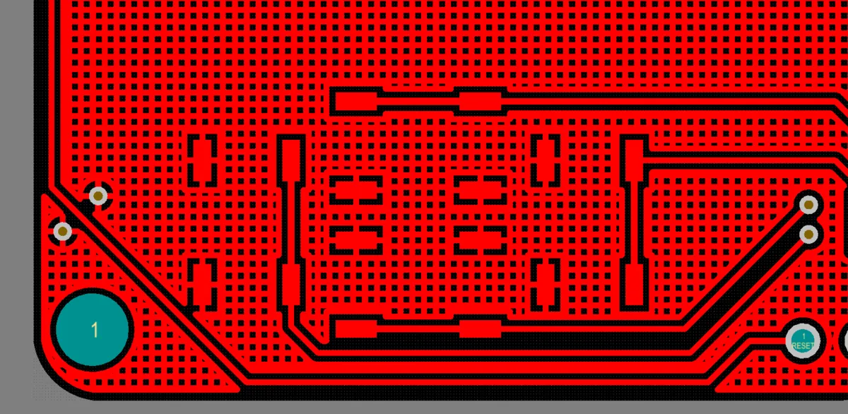
基板上に大きなGNDエリアを作成するために使用されるポリゴン配置(明るい赤)

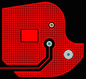
ポリゴン配置は実体とハッチングで表示され、クリアランスと制御された接続スタイル、エアギャップが異なることを示しています。
ポリゴン配置は、より単純なプリミティブオブジェクト、つまり領域またはトラックとアークから構成されるグループ設計オブジェクトです。ポリゴン配置は、領域オブジェクトを使用するか、トラックとアークオブジェクトの組み合わせを使用して、PCBレイヤー上に実体またはハッチング(格子)エリアを作成するために使用されます。銅プアとも呼ばれるポリゴン配置は領域と似ていますが、既存のオブジェクトの周りに自動的にプアされ、ポリゴン配置と同じネット上のオブジェクトにのみ接続するため、基板の不規則な形状のエリアを埋めることができます。
信号層では、大きな電源電流を運ぶエリアを定義するために実体のポリゴン配置を配置したり、電磁シールドを提供するために接地接続エリアとして使用することができます。ハッチングされたポリゴン配置は、アナログ設計で接地目的に一般的に使用されます。
信号層に配置されたポリゴン配置は、実体またはハッチングされた銅の多角形(多辺)エリアを作成します。プアされると、ポリゴンは異なるネットに属する電気オブジェクトの周りにクリアランスを自動的に許可し、同じネットのオブジェクトに接続し、不規則な形状のエリアを埋めます。クリアランスと接続プロパティは、適用される電気クリアランスとポリゴン接続スタイルの設計ルールによって制御されます。
ポリゴン配置は非銅層にも使用できます。ポリゴン配置が非信号層に配置される場合、それらはネットに割り当てられていないため、既存のオブジェクトの周りにプアされません。
ポリゴン配置の配置
ポリゴン配置はPCBエディターでのみ配置できます。直接ポリゴン配置を配置するには、まず必要なレイヤーに切り替えます。ポリゴン配置配置コマンド(Place » Polygon Pour)を起動すると、カーソルが十字線に変わり、ポリゴン配置配置モードに入ります。カーソルを位置させ、クリックするかEnter を押して配置します。さらにポリゴン配置を配置するか、右クリックまたはEsc を押して配置モードを終了します。
-
Altium DesignerのPCBエディターでは、実体領域、基板形状、またはポリゴン配置など、任意の多角形オブジェクトを定義するプロセスは同じです。実体オブジェクトは閉じたオブジェクトなので、配置プロセスを通じてどれだけ進んでいても、Altium Designerはカーソルからオブジェクトの開始位置に戻る線を表示します。この線は、右クリック(またはEscを押す)で配置モードを終了すると、実体オブジェクトの最後のエッジになります。配置プロセスは、多角形オブジェクトのアウトラインを定義するプロセス、つまり、利用可能なコーナーモードを使用してコーナーの位置を定義するプロセスです。
-
配置中にTab キーを押すと、配置を一時停止してプロパティ パネルにアクセスでき、配置中のポリゴン配置のプロパティ、充填およびネット接続オプション、プアアラウンドプロパティをその場で変更できます。一時停止ボタンオーバーレイ(
 )をクリックして配置を再開します。アウトラインが完成すると、ポリゴンはプロパティパネルで選択されたオプションに従って自動的に充填されます。ポリゴン配置プロパティセクションを参照してください。
-
ポリゴン配置は、選択されたプリミティブから作成することもできます。既存のポリゴンは、2つ以上のポリゴンに分割することができます、2つ以上のポリゴン配置オブジェクトを結合することができます、そして1つ以上のポリゴン配置オブジェクトを別の「ベース」ポリゴン配置から減算することができます。詳細については、対応するセクションを参照してください。
コーナーモード
ポリゴン配置を配置する際には、5つの利用可能なコーナーモード(45°、45°アーク、90°、90°アーク、および任意角度)があり、そのうち4つにはコーナー方向のサブモードもあります。配置中:
-
Shift+Spacebarを押して利用可能なコーナーモードを切り替えます。
-
Spacebarを押して2つのコーナー方向サブモード(任意角度モードを除く)を切り替えます。
-
アークコーナーモードのいずれかで、, または . キー最後の角を削除するには、Backspaceキーを押します。
-
2つのエッジを1クリックで配置するか、1つのエッジを1クリックで配置するかを切り替えるには、1のショートカットキーを押します。2番目のモードでは、点線のエッジは先読みセグメントと呼ばれます(下のセットの最後の画像に示されています。詳細については、先読み機能の理解セクションを参照してください)。

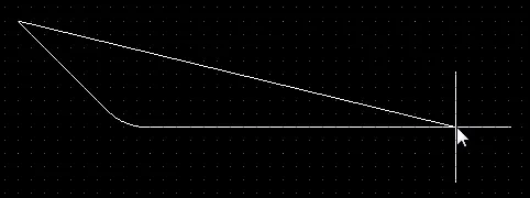


Shift+Spacebarを押して、利用可能な5つの角モードを切り替えます。2つのエッジまたは1つのエッジの配置を切り替えるには、1のショートカットを押します。
先読み機能の理解
PCB設計中には、将来のトラックセグメントやオブジェクトエッジがどこに配置される必要があるかを予測できる必要がある状況が多くあります。この要件をサポートするために、Altium Designerには先読みと呼ばれる機能が含まれています。先読みが有効になっている場合、カーソルに現在接続されているトラック/オブジェクトエッジはクリック時に配置されず、前のセグメントのみが配置されます。言い換えると、最後のセグメントによって、将来のセグメントがどこに配置されるかを先読みすることができます。
オブジェクト配置中に1のショートカットキーを押して、先読みをオンまたはオフに切り替えます。各モードを表示する方法に注目してください。トラック配置では、次のクリックで配置されるセグメントがハッチング表示され、先読みセグメントは空または空洞として表示されます。固体オブジェクト配置では、次のクリックで配置されるエッジが白い実線として表示され、先読みエッジは白い点線として表示されます。
次の画像は、先読み機能がオンとオフの場合のトラックセグメントの表示の変化を示しています。
とオフにしたトラック配置(2番目の画像)。次のマウスクリックでハッチングされたトラックセグメントが配置されます。") 先読みをオンにしたトラック配置(最初の画像)とオフにしたトラック配置(2番目の画像)。次のマウスクリックでハッチングされたトラックセグメントが配置されます。
先読みをオンにしたトラック配置(最初の画像)とオフにしたトラック配置(2番目の画像)。次のマウスクリックでハッチングされたトラックセグメントが配置されます。
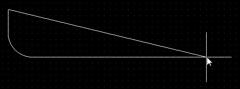
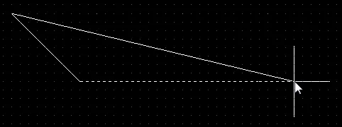
先読み機能は、ポリゴン配置配置中にも機能します。配置中に1のショートカットキーを押してオンまたはオフに切り替えます(このショートカットはオブジェクト配置中にのみ機能します)。次の画像は、ポリゴン配置の最初の角の配置を示しています。
 先読みがオンです。次のマウスクリックで、実線がポリゴンエッジになりますが、点線はそうなりません。実線の戻り線に注目してください。これは、ポリゴン配置を終了した場合にポリゴンがどのように閉じられるかを示しています。
 先読みがオフです。次のクリックで、実線の両方がポリゴンエッジになります。実線の戻り線に注目してください。これは、ポリゴン配置を終了した場合にポリゴンがどのように閉じられるかを示しています。
ポリゴンの編集
ポリゴン配置の移動
選択したポリゴン配置の実際の形状(編集ハンドルから離れた場所)をクリックしてドラッグすると、移動します。Shiftキーを押しながら複数のポリゴン配置を選択して移動します。
移動中に実行できる追加のアクションは次のとおりです:
-
Spacebarを押してポリゴン配置を反時計回りに回転させるか、Shift+Spacebarを押して時計回りに回転させます。回転は、PreferencesダイアログのPCB Editor – Generalページで定義されたRotation Stepの値に従います。
-
Lキーを押してポリゴンをボードの反対側に反転させます。
-
X軸またはY軸に沿ってポリゴンをミラーリングするには、XキーまたはYキーを押します。
または、ポリゴン配置の上で右クリックしてコンテキストメニューからPolygon Actions » Move Polygonコマンドを選択します。コマンドを起動すると、ポリゴン配置がカーソルにアウトラインモードでアタッチされます。必要な位置にポリゴン配置を移動し、クリックまたはEnterを押して配置を行います。
ポリゴン配置の形状変更
 90ºのアークコーナーを持つポリゴン配置のサイズ変更。
選択したポリゴン配置には、ポリゴン配置の形状を編集するための2種類のポイントまたは「ハンドル」が含まれています。
既存のポリゴンは、各角または各辺の中心に位置するこれらのハンドル、または頂点を移動することで形状を変更できます。
ポリゴンの形状を変更するには:
-
ポリゴンをクリックして選択すると、ポリゴンの頂点が強調表示され、カーソルが十字線に変わります。
-
フルハンドルをクリックして押さえ、その角を移動します。
-
辺に沿ってクリックして押さえ、ドラッグすると、その全体の辺を移動できます。
-
空のハンドルをクリックして押さえ、ドラッグすると、全体の側面(トラックおよびアークの場合)を移動できます。
-
Ctrl+クリック で空のハンドルを押すと、その辺を2つの辺に分割できます。 Ctrl は移動の開始時にのみ押さえる必要があります。その後、Shift+Spacebar ホットキーを使用して、モード(アーク、マイター、任意の角度)を切り替えることができます。

上の画像は空のハンドル編集を示しています。下の画像では、Ctrl を押しながらハンドルを掴んで編集のために移動しています。
-
「任意の角度」配置モードが望ましくない頂点を作成した場合、頂点をクリックして押さえ、その辺の頂点を1つに減らすためにドラッグします。頂点を削除するには、それを移動するかのように頂点をクリックして押さえ、Delete キーを押します。

-
完了したら、右クリックしてから Polygon Actions » Repour Selected を選択して、新しい形状のポリゴンを再注ぎします。
ポリゴン配置ボーダーの変更
頂点編集に加えて、Polygon Actions » Modify Polygon Border 右クリックコマンドを使用して、ポリゴンの形状を簡単に変更することもできます。このコマンドを起動すると、カーソルが十字線になります。クリックするたびに新しい頂点が追加されます。ポリゴン配置中と同様に、Shift+Spacebar ショートカットを使用して角の形状を変更できます。
ポリゴン配置のサイズ変更
選択されたポリゴン配置オブジェクトの形状を編集するからサイズを編集するには、選択されたポリゴン配置オブジェクト上で右クリックし、コンテキストメニューから Polygon Actions » Resize Polygon コマンドを選択します。このコマンドを起動すると、ポリゴン編集モードは形状の再形成からサイズ変更に変わります。これは、ポリゴン形状の各辺に沿った編集ハンドルが、オブジェクトの境界矩形の角(および中心)に位置する8つの編集ハンドルに置き換えられることによって視覚的に確認できます。
ポリゴン配置のサイズまたは位置を変更した後、それは変更されたとマークされます。Repour Polygons After Modification オプションが Preferences ダイアログのPCB Editor - General ページで有効にされている場合、ポリゴン(およびそのすべての依存オブジェクト)は自動的に再注ぎされます。このオプションが有効でない場合、ポリゴン配置は再注ぎされません。
サイズの編集から形状の編集に戻るには、現在サイズが変更されている選択されたポリゴン配置オブジェクト上で右クリックし、コンテキストメニューから Polygon Actions » Edit Polygon Shape コマンドを選択します。
ポリゴン配置プロパティ

Properties パネルのPolygon Pour モード
| アクション |
-
Repour – ポリゴンを再配置するにはクリックします。この機能は、ポリゴン内の設計を変更した場合に便利です。復元された後、設計変更によって作成された違反をクリアするために再注ぎする必要があります。
-
Shelve – ポリゴンを棚上げするにはクリックします。これは、設計からポリゴンを削除するのではなく、表示、DRC、およびネット接続分析エンジンから隠します。
-
Assign net – 希望するポリゴンにネットを割り当てるにはクリックします。選択されると、ネット名ダイアログが表示されます。
-
Bring to front – 選択したポリゴンが他の重なるポリゴンよりも前面に来るように(最高の優先順位を持つように)注ぎ順を変更するにはクリックします。
-
Send to back – 選択したポリゴンが他の重なるポリゴンの後ろに来るように(最低の優先順位を持つように)注ぎ順を変更するにはクリックします。
-
Modify – PCBドキュメント自体からポリゴンの形状を再定義するにはクリックします。
|
| ネット情報 |
ポリゴン配置が属するネットに関する情報、およびそのネットがメンバーである場合の差動ペア。適切な場合はクラス情報も表示されます。PCB配置&編集テクニックページを参照して、ネット情報についてさらに学びましょう。 |
| ネット |
このポリゴン配置がメンバーであるネット。アクティブなボード設計のすべてのネットがドロップダウンリストにリストされます。No Netを選択して、ポリゴンがどのネットにも接続されていないことを指定します。デザインルールチェッカーがPCBオブジェクトが合法的に配置されているかどうかを判断するために使用されるプリミティブのNetプロパティ。または、Assign Netアイコン( )をクリックしてデザインスペース内のオブジェクトを選択 - そのオブジェクトのネットが選択されたポリゴンに割り当てられます。PCB配置&編集テクニックページを参照して、オブジェクトにネットを割り当てる方法についてさらに学びましょう。 )をクリックしてデザインスペース内のオブジェクトを選択 - そのオブジェクトのネットが選択されたポリゴンに割り当てられます。PCB配置&編集テクニックページを参照して、オブジェクトにネットを割り当てる方法についてさらに学びましょう。 |
| レイヤー |
ドロップダウンを使用して、ポリゴン配置が配置されるレイヤーを選択します。 |
| 名前 |
ポリゴンに適切な名前を指定します。ポリゴンを識別するのに役立つだけでなく、設計ルールで特定のポリゴン(またはポリゴンのファミリー)をターゲットにするために名前を使用することができます。デフォルトでは、レイヤーとネットに基づいて自動的にポリゴンの命名が適用されます。命名は、PropertiesパネルのBoardモードのPolygon Naming Schemeフィールドで指定された命名スキームに基づいています。カスタム名を入力して自動命名に戻したい場合は、単にフィールドをクリアしてEnterを押します。
-
カスタム命名をクリアして自動命名を使用するように戻す操作は、PCB ListパネルおよびPolygon Pour Managerからも実行できます。
-
自動割り当てされた名前は、Altium Designerによって継続的に監視および管理されます。ネット割り当てやレイヤースタック内のレイヤーの位置などの属性が変更されると、自動割り当てされた名前は自動的に更新されます。影響を受ける設計ルールも自動的に更新されます。
|
| 面積 |
与えられたポリゴン配置が囲む面積が平方ミリメートルまたは平方インチでリストされます。 |
| (X/Y) |
このポリゴン配置の最初の頂点の現在の設計空間内の位置、ユーザー定義の原点に対する相対位置です。 ボタンをクリックして、このポリゴン配置の位置をロックします。PCB配置&編集テクニックページを参照して、設計オブジェクトをロックする方法についてさらに学びましょう。 ボタンをクリックして、このポリゴン配置の位置をロックします。PCB配置&編集テクニックページを参照して、設計オブジェクトをロックする方法についてさらに学びましょう。 |
| 塗りつぶしモード |
ポリゴン配置の塗りつぶしモードを選択します。利用可能な3つのモードがあり、それぞれに独自の利点とオプションがあります。ポリゴン配置塗りつぶしモードについてさらに学びましょう。 |
| 同じネット上での注ぎ |
同じネット上のオブジェクトに遭遇したときの配置挙動を制御するためにドロップダウンを使用します。ポリゴン配置をネットに接続するについてさらに学びましょう。 |
| デッドコッパーの除去 |
ポリゴンを塗りつぶす際、他のトラックやパッドなどの存在により、ポリゴンの一部(島)が接続されたネットから完全に孤立してしまうことがあります。このオプションを有効にすると、他のネットオブジェクトに少なくとも1つの接続を含まないポリゴンのエリアは自動的に削除されます。ポリゴンが割り当てられたネット上のパッドを一つも囲んでいない場合、それは全てデッドコッパーとみなされ、全て削除されます。この状況では、ポリゴンがこの位置に存在することを示すために、ポリゴンのアウトラインが表示されます。 |
| 最適なボイド回転 |
このオプションを有効にすると、ポリゴンが他のネットに属する隣接オブジェクトの間を通過する際に、最大のネック幅を得るようにポリゴンの端が配置されるようになります。ポリゴンのアークは短い直線エッジに置き換えられ、その長さはArc Approx設定によって決定されます。 |
| アウトライン頂点 |
この領域を使用して、現在選択されているポリゴン塗りつぶしオブジェクトの個々の頂点を変更します。既存の頂点の位置を変更したり、新しい頂点を追加したり、必要に応じて削除することができます。頂点間のアーク接続を定義でき、頂点情報をCSV形式のファイルにエクスポートおよびインポートするためのサポートが提供されています。
-
頂点グリッド – ポリゴン塗りつぶしのために現在定義されている全ての頂点をリストします。
-
Index – 頂点の割り当てられたインデックス(編集不可)。
-
X – 頂点のX(水平)座標。クリックして編集。
-
Y – 頂点のY(垂直)座標。クリックして編集。
-
Arc Angle (Neg=CW) – この頂点から次の頂点へ接続するアークの角度。デフォルトでは、このフィールドは空白のままで、接続は直線エッジです。クリックして編集し、必要に応じてアーク角度を入力します。正の値を入力すると、反時計回りのアークが描かれます。時計回りのアークを描くには、負の値を入力します。
-
Add – 新しい頂点を追加するために使用します。新しい頂点は現在選択(ハイライト)されている頂点エントリの下に追加され、最初は以前選択されたエントリと同じ座標を持ちます。
-
 – 現在選択されている頂点エントリを削除するためにクリックします。削除が行われる前に確認が求められます。 – 現在選択されている頂点エントリを削除するためにクリックします。削除が行われる前に確認が求められます。
グリッドの全内容をCSV形式のファイルにエクスポートするには、グリッド内の任意の場所で右クリックし、Export To CSVコマンドを選択します。Export Outline Verticesダイアログが表示され、ファイルを保存する場所と名前を決定します。デフォルトでは、ファイルはOutline Vertices.CSVという名前で保存されます。CSVファイルから頂点情報をインポートするには、グリッド内の任意の場所で右クリックし、Import From CSVコマンドを選択します。Import Outline Verticesダイアログが表示され、必要なCSVファイルを参照して開きます。インポートすると、現在グリッドに定義されている内容が上書きされることに注意してください。
|
CSVファイルからのデータのインポート、または手動での変更が行われた場合 – Propertiesパネルの上部に青いバナーが表示され、変更を適用するように促されます。
ポリゴン塗りつぶしモード
を使用して配置した後、トラック/アーク(Hatched)を使用して配置する。")
同じポリゴンを領域(Solid)を使用して配置した後、トラック/アーク(Hatched)を使用して配置する。
ポリゴン塗りつぶしエンジンは、Propertiesパネルで選択された塗りつぶしモードに応じて、ソリッド領域またはトラックとアークの組み合わせからポリゴンを構築できます。プレビュー画像はソリッドポリゴン塗りつぶしのグラフィカルな表現に変わり、パネルには関連するオプションが提供されます。サポートされている塗りつぶしモードは3つあります。
各塗りつぶしモードオプションは、Show Preview / Hide PreviewオプションをPropertiesパネルに表示します。パネル内で選択したポリゴンの視覚表現を表示または非表示にするために使用します。
ソリッド
このモードが選択されると、ポリゴンは内部的にソリッド領域オブジェクトから構築され、完成したポリゴンの各連続する銅領域に対して別々の領域があります。
このタイプのポリゴンは、Gerber領域定義を使用してGerberに出力されます。プロパティパネルの設定。このタイプのポリゴンは、配置されるオブジェクトがはるかに少なくなるため、ファイルサイズが小さくなり、配置と再描画、ファイルの開き、DRCおよびネット接続分析が速くなり、GerberおよびODB++で完全にサポートされている領域オブジェクトのため、出力ファイルも小さくなります。
このモードが選択されたときにプロパティパネルで提供される関連オプションは次のとおりです - ![]() 画像を表示。
画像を表示。
| 指定した面積より小さい島を削除 |
面積値を指定します。この値より小さい銅のエリアは削除されます。
このオプションは面積ベースのみで、その島がパッドやビアに接続されているかどうかは考慮しません。すべての接続されていない銅のエリアは、Remove Dead CopperオプションがPropertiesパネルで有効になっている場合は常に削除されます。
|
| アーク近似。 |
完璧なアーク(曲線のエッジは複数の短い直線エッジから作成されます)からの最大偏差を指定します。この値を小さくすると、より多くの直線エッジが使用されてアークのより良い近似が得られます。 |
| 指定した幅より小さいネックを削除 |
幅値を指定します。この値より小さい幅の銅の細片は削除されます。このオプションの値が大きい場合、ポリゴンが配置できない狭い場所がより多くなります。通常、これは設計で使用される最小幅のトラックまたは製造業者がサポートする最小の銅幅よりも小さく設定されません。Obey Rulesオプションを有効にして、適用可能な最小幅制約から値を取得します。 |
ハッチング
このモードが選択されると、ポリゴンはトラックとアークオブジェクトから作成されます。ハッチングされたポリゴンのアウトラインは、ポリゴンのユーザー定義エッジがアウトライントラックとアークの中心線になるように、トラックとアークで作成されます。
このタイプのポリゴンは一般的に配置が遅く、PCBおよびGerberファイルサイズが大きくなります。ハッチングされたポリゴンは、アナログ設計でよく使用されます。
このモードが選択されたときにプロパティパネルで提供される関連オプションは次のとおりです - ![]() 画像を表示。
画像を表示。
| トラック幅 |
ポリゴンを作成するために使用されるトラックの幅を指定します。 |
| グリッドサイズ |
ハッチングされたポリゴンのトラックが配置される間隔、またはグリッドを指定します。
Track WidthとGrid Sizeの設定を調整することで、完成したポリゴンはハッチングされた(Track WidthがGrid Sizeより小さい)またはソリッド(Track WidthがGrid Sizeと等しいかそれ以上)の外観になります。
|
| パッドを囲む形状を指定 |
パッドを囲むために使用される形状を指定します:ArcsまたはOctagons。 |
| ハッチモード |
利用可能なモードは4つあります:90 Degree、45 Degree、Horizontal、またはVertical。 |
| 最小プリム長 |
塗りつぶしモードで許可されるトラック/アークオブジェクトの最短長を指定します。 |
| ポリゴンカットアウトに従う |
ハッチングされたポリゴンの配置がポリゴン塗りつぶしカットアウトの境界を侵害しないようにこのオプションを有効にします。このオプションが無効の場合、ポリゴン塗りつぶしトラックの中心線はポリゴン塗りつぶしカットアウトの境界に沿って配置されます。 |
なし
このモードは基本的にHatchedモードと同じです。しかし、塗りつぶしのトラックとアークは追加されません。
このモードは、さまざまなポリゴンの構造と設計を分析し、重なり合うポリゴンの相互作用を理解しようとする場合に便利です。また、設計変更が行われており、ポリゴンがプロセスに干渉している場合にも便利です。設計変更中にアウトラインを使用する代わりのアプローチとして、ポリゴンを
棚上げすることができます。これにより、PCBファイルに保持されますが、表示からは削除されます。
このモードが選択されたときにプロパティパネルで提供される関連オプションは次のとおりです - ![]() 画像を表示:
画像を表示:
| Track Width |
ポリゴン配置アウトラインのトラック幅を指定します。 |
| Surround Pad With |
パッドを囲む形状 (ArcsまたはOctagons) を指定します。 |
| Min Prim Length |
塗りつぶしモードのトラック/円弧オブジェクトの長さを指定します。 |
| Obey Polygon Cutout |
このオプションは、ポリゴン配置 がポリゴン配置カットアウトの境界を侵さないようにする場合に有効にします。このオプションを無効にすると、ポリゴン配置トラックの中心線は、ポリゴン配置の切り欠きの境界に沿って配置されます。 |
ポリゴン配置をネットに接続する
ポリゴンはネットにアタッチできます。Netドロップダウンで必要なネットを選択し、Propertiesパネルで設定します。ポリゴン配置は、ポリゴンのアウトライン内に見つかったこのネットの各パッドとビアに接続され、適用されるポリゴン接続スタイル設計ルールに従います。ルールは、必要に応じて、スルーホールパッド、SMDパッド、ビアの接続方法を異なる方法で定義することをサポートしています。ポリゴンと他のネットに属するオブジェクトとのクリアランスは、適用される電気的クリアランス設計ルールによって決定されます。
ポリゴン配置が同じネット上の他のオブジェクト(配線トラック、アーク、塗りつぶし、領域)をどのように扱うかは、ポリゴン配置が選択されたときにPour Over Same Netドロップダウンで選択されたオプションによって決定されます:Propertiesパネルで設定します:
-
Don't Pour Over Same Net Objects – このオプションを選択すると、ポリゴンがこの(または他の)ネットのトラック、アーク、塗りつぶし、領域、またはポリゴンオブジェクト上に配置されることを望まない場合、つまりポリゴンを自由空間にのみ配置することを選択します。
-
Pour Over All Same Net Objects – ポリゴンを自由空間だけでなく、ポリゴンのエリア内にある同じネット上のすべてのオブジェクト(つまりトラック、アーク、塗りつぶし、領域、他のポリゴン)上にも配置したい場合は、このオプションを選択します。例えば、そのネット上の既存のルートはポリゴンによって完全に覆われます。
-
Pour Over Same Net Polygons Only – ポリゴンを自由空間と、その境界内にある同じネットに属する既存のポリゴン配置オブジェクト上にのみプアしたい場合は、このオプション(デフォルト)を選択します。ポリゴンは、どのネットに属しているかに関係なく、他のすべてのオブジェクト(トラック、アーク、塗りつぶし、領域)の周りに配置されます。
ポリゴン配置が非信号層に配置された場合、これらのオブジェクトはネットに割り当てられておらず、したがって何にも属していないため、既存のオブジェクトの周りには配置されません。
ポリゴン配置の棚卸しと復元
設計プロセス中に変更が発生するのは普通のことです – コンポーネントが追加されたり変更されたり、配線が更新される必要がある等です。このプロセス中に既存のポリゴンを管理することを簡素化するために、それらを棚卸しすることができます。これにより、表示から一時的に隠され、DRCおよびネット接続性分析エンジンからは除外されますが、PCBデータベースには保持されます(つまり、破壊されず、いつでも復元できます)。これにより、視覚的な容易さと、視覚的なポリゴン配置がもたらすことがあるパフォーマンスへの影響 – 編集およびDRCの両方 – を避けながら、ボードレイアウトの変更を行うことができます。
-
現在の設計で全てのポリゴン配置を棚卸しするには、メインメニューからTools » Polygon Pours » Shelve <n> Polygon(s)を選択します(<n>は、設計で検出されたポリゴン配置の数です)。
-
全ての棚上げされたポリゴン配置を復元するには、メインメニューからTools » Polygon Pours » Restore <n> Shelved Polygon(s)コマンドを選択します(<n>は現在棚上げされているポリゴン配置の数です)。復元された全てのポリゴンは、変更されたものとして扱われます。Repour Polygons After ModificationオプションがPreferencesダイアログのPCB Editor - Generalページで有効になっている場合、ポリゴン配置とその依存関係にある全てが自動的に再配置されます。このオプションが無効の場合、復元されたポリゴン配置は再配置されません。
-
右クリックPolygon ActionsサブメニューコマンドやPolygon Pour Managerダイアログから、ポリゴンを選択的に棚上げすることもできます。
ポリゴンの再配置
ポリゴン内のデザインを変更した場合、復元された後、デザイン変更によって作成された違反をクリアするために再配置する必要があります。現在のドキュメントでポリゴンを再配置(再構築)する方法はいくつかあります。
ポリゴンを再配置するには、ポリゴンを右クリックしてRepourコマンドをPolygon Actionsサブメニューから選択するか、RepourコマンドをTools » Polygon Poursサブメニューで使用します:
-
Repour Selected - 選択された全てのポリゴン配置(およびその依存関係にあるもの)を再配置します。
-
Repour All - 定義された(および棚上げされていない)全てのポリゴン配置を再配置します。
-
Repour Violating Polygons - 違反している全てのポリゴン配置を再配置します。
-
Repour Modified - 変更されたがまだ再配置されていない全てのポリゴン配置を再配置します。変更されたポリゴン配置は、何らかの方法で変更されたが、まだ再配置されていないものです。そのIsModifiedプロパティは、選択されたポリゴン配置のPCB Listパネルから確認でき、有効(True)になっています。
Polygon Pour Managerダイアログ(Tools » Polygon Pours » Polygon Manager)でも、必要なポリゴンを選択してRepourボタンをクリックすることでポリゴン配置を再配置できます。
Confirmダイアログで変更を確認します。
ポリゴンを編集するには、ポリゴンが存在するレイヤーが現在のまたはアクティブなレイヤーである必要があります。
Repour Polygons After ModificationおよびRepour all dependent polygons after editingオプションがPreferencesダイアログのPCB Editor - Generalページので有効になっている場合、ポリゴン配置およびその全ての依存関係にあるものは、変更後に自動的に再配置されます。
配置順序の設定
2つのポリゴンが重なる場合、Altium Designerはどちらのポリゴンが重なっている領域を占有するべきかを知る必要があります。これは、配置順序を定義することによって行われ、順序が高いポリゴンが優先され、重なっている領域に配置されます。重なっているポリゴンの配置順序は、選択したポリゴン塗りつぶし上で右クリックして、コンテキストメニューから以下のコマンドのいずれかを選択することによって対話的に設定できます:
変更された順序は、修正されたと見なされるポリゴン塗りつぶしが再配置されると、設計スペースで視覚的に確認できます。
ポリゴン接続スタイルの制御
メインページ: Polygon Connect Style Design Rule
ポリゴンが接続されているネット上のパッドにどのように接続するかは、適用されるPlane » Polygon Connect Styleデザインルール(Design » Rules)によって制御されます。

ポリゴンがネット上のパッドにどのように接続するかは、Polygon Connect Styleデザインルールによって決定されます。
3つの接続オプションが利用可能です:
-
Relief Connect - スポークスタイルの接続が作成されます。導体のNumber、これらの導体のAngle(90ºまたは45º)、Conductor Width、およびAir Gap Width (パッドの端とパッドを囲むポリゴンの端との間のクリアランス)を定義します。
-
Direct Connect - ポリゴンがパッド上に配置され、ピンへの固体銅を作成します。
-
No Connect - ネット上のパッドはポリゴンから隔離されます。
Air Gap Width設定は、パッドの端と周囲のポリゴンとの間のクリアランスを制御しますが、以前のバージョンのAltium DesignerではElectrical Clearanceデザインルールがこれを行っていました。以前のバージョンのAltium Designerで設計されたボードを開いたときに警告が表示される場合、この状況ではPolygon Connect StyleデザインルールのAir Gap Width設定を確認して設定することが重要です。
ポリゴンクリアランスの制御
メインページ:Clearance Design Rule
信号(銅)層に配置された任意のオブジェクトと同様に、ポリゴンが配置されたオブジェクトからのクリアランスは、適用されるElectrical Clearanceデザインルールによって制御されます。
 ポリゴンから他のネットのオブジェクトへのクリアランスは、Electrical Clearanceデザインルールによって制御されます。
ポリゴンと他のネットオブジェクトとの間により大きなクリアランスを持つことは一般的な慣習です。これを実現するために、ポリゴン固有のElectrical Clearanceデザインルールを定義できます。これの例は上の画像に示されています。Polygon Clearanceルールは、任意の一般的なクリアランスルールよりも高いPriorityを持つ必要があります。
ポリゴン用のElectrical Clearanceルールを定義する場合、IsPolygon(またはIsPoly)のクエリキーワードではなく、InPolygon(またはInPoly)を使用する必要があります。これは、クリアランスルールがポリゴン全体のオブジェクトではなく、ポリゴンを構成するプリミティブ(領域、トラック、アーク)に対して操作するためです。InPolygonオブジェクトとAll他のオブジェクトとの間の有効なクリアランスルールになります。
ポリゴン塗りつぶしカットアウト
ポリゴン塗りつぶしカットアウトは、基本的にポリゴン内に定義された空洞または穴である負の銅領域です。ポリゴンにカットアウトを定義するには:
-
メインメニューからPlace » Polygon Pour Cutoutコマンドを選択します。
-
カーソルが十字線に変わり、ポリゴンの境界内から開始します。クリックして開始位置を定義します。
-
ポリゴンを横切ってカーソルを移動します。Shift+Spacebarを押して、領域の角のモードを切り替えます。
-
クリックしてマウスを動かし、カットアウトの輪郭を定義し続けます。
-
右クリックしてポリゴンカットアウト配置モードを終了します。
-
元のポリゴンは再度プアされる必要があります。それを選択するためにクリックし、メインメニューからTools » Polygon Pours » Repour Selectedコマンドを使用します - 新しいカットアウトの周りにプアされます。
カットアウトは実際には領域オブジェクトで、Polygon Cutoutオプションが有効になっています。必要に応じて移動、サイズ変更、または削除できます。カットアウトのサイズを変更するには、一度クリックして選択し、クリックして保持し、エッジまたは頂点をドラッグします。カットアウトが変更されるたびにポリゴンを再配置する必要があることを覚えておいてください。
; ポリゴンが再配置されました(2番目の画像)。")
カットアウトが配置されました(最初の画像); ポリゴンが再配置されました(2番目の画像)。
トラックのセットからポリゴン配置を作成する
電気銅の領域を定義するだけでなく、ポリゴンやソリッド領域は、特別なシンボルや会社のロゴなど、他の多角形のデザインオブジェクトを定義するためにも使用されます。必要な形状のアウトラインがAutoCADなどの別の設計ツールで定義されている場合、DXFファイルとしてエクスポートしてからAltium Designerにインポートできます。そのアウトラインはその後、ポリゴンまたはソリッド領域に変換できます。
選択したトラックおよび/またはアークオブジェクトで構成される閉じた境界をポリゴンに変換するには、閉じた形状を形成するすべてのプリミティブを選択し、メインメニューからTools » Convert » Create Polygon from Selected Primitivesを選択します。
注意点:
-
ポリゴンは現在の(またはアクティブな)レイヤーに作成され、選択されたトラックがあるレイヤーではありません。これは、メカニカルレイヤーで形状を定義してから、信号レイヤーでポリゴンを作成できることを意味します。
-
元々選択されたプリミティブは削除されません - ポリゴンが作成された後も存在し、選択されたままになります。新しいポリゴンは選択されたオブジェクトの内側にプアされます。
-
新しいポリゴンのエッジは、それを作成するために使用された選択されたオブジェクトの中心線に沿って配置されます。
-
ポリゴンが選択されたトラックと同じレイヤー上に作成される場合、適用されるElectrical Clearance設計ルールに従ってトラック内にプアされます。
-
ポリゴンはその塗りつぶしモードがNoneに設定されて作成されます。新しいポリゴンをソリッドまたはハッチで再配置するにはダブルクリックします。
Create Polygon from Selected Objectsアルゴリズムは選択されたオブジェクトの中心線を使用するため、接触するオブジェクトの終端と開始位置が正確に一致している(同じX、Y位置で開始/終了する)必要があります。そうでない場合、アルゴリズムが失敗した位置を示すConfirmダイアログが表示され、アルゴリズムにオブジェクトのエッジからポリゴンを定義するよう指示する機会も提供されます。選択されたオブジェクトがわずかに重なっている限り、このオプションは選択されたオブジェクトの外側のエッジをたどるポリゴンのエッジを作成するはずです。
ポリゴン配置のスライス
単一のポリゴン配置は、2つ以上の別々のポリゴン配置にスライスできます。これを行うには:
-
スライサーが機能するためには、現在のレイヤーがポリゴン配置が存在するレイヤーである必要があるため、正しいレイヤーを現在のレイヤーに設定します。
-
メインメニューからPlace » Slice Polygon Pour (またはActive Bar上のSlice Polygon Pourコマンド、またはポリゴン配置の右クリックメニューからのPolygon Actions » Slice Polygon Pourコマンド)を選択します。
-
コマンドを選択すると、スライスモード(トラック配置モードに似ています)になり、カーソルが十字線に変わります。ポリゴンの境界の外側から始めて、スライスラインの開始点(最初ポリゴン上をカーソルを移動させます。スライスプロセスでは、ライン配置モードを使用してスライスのパスと幅の両方を定義します。スライスを定義する際には:
-
Shift+Spacebarを押して、ライン配置のコーナーモードを切り替えます。
-
Spacebarを押して、スタートとエンドのコーナーモードを切り替えます。
-
Backspaceを押して、最後に配置したコーナーを削除します。
-
Tabを押して、Line Constraintsダイアログにアクセスし、ラインの幅や配置中の現在のレイヤーを変更します。

Line Constraintsダイアログ。
-
Line Width - このフィールドを使用して、ラインの新しい幅を入力します。この新しい幅は、現在配置中のセグメントに適用されます。
-
Current Layer - このフィールドを使用して、ラインが配置されるレイヤーを切り替えます。ドロップダウンメニューには、ボードに対して現在定義されている(および有効になっている)すべてのレイヤーがリストされています。選択されたレイヤーは、現在配置中のセグメントの次のセグメント、つまり先読みセグメントに適用されます。
-
クリックして、スライスラインを定義する一連の頂点をアンカーします。
-
ポリゴンを横切って反対側に配置されたスライスラインが配置されたら、右クリックまたはEscを押してライン配置を終了します。
-
もう一度右クリックしてスライシングを終了します。Confirmダイアログが表示され、ポリゴンを分割するかどうかを尋ねられます。Yesをクリックして分割します。
これで、2つの独立したポリゴンができたので、必要に応じてそれぞれを編集および再配置できます。
スライスラインがポリゴンの配置と同じ色であるため、スライスプロセスを開始する前に、スライスラインが容易に見えるように、配置モードをNoneに設定してポリゴンを再配置すると便利です。
分割されたポリゴンセクションは実際には変更されたとマークされていないため、変更されたポリゴンの再配置を行っても効果はありません。分割を最終化し、設計スペースで視覚的に確認するには、ポリゴンの「部分」を選択してRepour Selectedコマンドを使用するか、Repour Allコマンドを使用して、手動で再配置する必要があります。
選択したポリゴン塗りつぶしの結合
2つ以上のポリゴン塗りつぶしオブジェクトは、次の一連のアクションを実行することで結合できます:
-
必要に応じて、新しい(または既存のポリゴン塗りつぶし)を重なるように配置またはドラッグします。
-
結合するポリゴン塗りつぶしをすべて選択します。
-
選択した配置の1つ上で右クリックし、コンテキストメニューからPolygon Actions » Combine Selected Polygonsコマンドを選択します。
新しいポリゴンのプロパティは、各衝突グループで最初に選択されたポリゴンからコピーされます。
選択したポリゴン塗りつぶしの減算
1つ以上のポリゴン塗りつぶしオブジェクトは、「ベース」となるポリゴン塗りつぶしから減算することができます。これを行うには、次の一連のアクションを実行します:
-
必要なベースポリゴン塗りつぶしに重なるように、新しいまたは既存のポリゴン塗りつぶしを配置またはドラッグします。これが「減算される」配置です。
-
ベースポリゴン塗りつぶしを選択し、右クリックして、コンテキストメニューからPolygon Actions » Subtract Polygons From Selectedコマンドを選択します。
-
減算するポリゴンを選択します。
-
右クリックまたはEscを押して、プロセスを完了します。
ポリゴン塗りつぶしをプリミティブに分解
ポリゴン塗りつぶしは、メインメニューからTools » Convert » Explode Polygon to Free Primitivesコマンドを選択するか、配置されたポリゴン塗りつぶし(選択されているかどうか)上で右クリックして、コンテキストメニューからPolygon Actions » Explode Polygon To Free Primitives(またはExplode Selected Polygons To Free Primitives)コマンドを選択することで、構成されていたさまざまなプリミティブに戻すことができます。実体ポリゴンは領域プリミティブに、ハッチングされたポリゴンはトラックとアークに戻ります。一度分解されると、ポリゴン塗りつぶしオブジェクトはもはやグループオブジェクトとして操作できなくなります。
分解されたポリゴンを再グループ化する実際のコマンドはありませんが、Undoコマンドを使用してこれを実現できます。
Polygon Pour Managerダイアログ
Polygon Pour Managerダイアログは、現在PCB設計スペースに存在するすべてのポリゴンの高レベルビューを提供します。このダイアログでは、各ポリゴンの名前を付ける/名前を変更する、ポリゴンの配置順序を設定する、選択したポリゴンに対して再配置または棚上げ動作を行う、選択したポリゴンに対して設計ルールを追加/適用することができます。
Polygon Pour Managerダイアログを開くには、メインメニューからTools » Polygon Pours » Polygon Managerコマンドを選択するか、設計スペース内に配置されたポリゴン配置上で右クリックしてコンテキストメニューからPolygon Actions » Polygon Managerコマンドを選択します。

Polygon Pour Managerダイアログは、設計内のすべてのポリゴンを完全に制御することができます。
コマンドを起動すると、Polygon Pour Managerダイアログが開きます。このダイアログでは、設計内のポリゴン配置のすべての非グラフィカル編集を行うことができます。これには以下のコントロールが含まれます:
-
ポリゴンの名前を変更する(自動命名機能を使用することもできます)。
-
ポリゴン配置の順序を設定する。
-
すべてまたは特定のポリゴン(変更された/選択された/違反している)の再配置を行う。
-
すべてまたは選択されたポリゴンを棚上げまたは棚上げ解除する。
-
すべてまたは選択されたポリゴンをロックまたはアンロックする。
-
すべてまたは選択されたポリゴンに対して違反を無視するか保持する(オンラインDRCに関して)。
-
ポリゴン接続スタイルとクリアランス設計ルールを追加/適用する。
-
選択されたポリゴンに対してポリゴンクラスを追加する。
-
選択されたポリゴンまたはボードのアウトラインから新しいポリゴンを作成する。
Polygon Pour Managerダイアログのオプションとコントロール
表示/編集
これは、PCBドキュメント内のすべての既存のポリゴンのリストです。プール順序リストは、レイヤーごとにポリゴンアウトをグループ化し、現在選択されているポリゴン配置(または異なるレイヤーで複数のプールが選択されている場合は最初に選択されたプール)と同じレイヤー上のポリゴンプールのみを表示します。列見出しをクリックしてその列でソートします。ポリゴン名は編集可能です。名前が付けられると、ポリゴンルールを適用するためやクエリを作成するために使用できます。グリッド内で1つ以上のポリゴンを選択する(Ctrl+クリック)と、以下に説明するグリッド機能を実行できます。
グリッド
-
Name – ポリゴンに適切な名前を指定します。ポリゴンを識別するのに役立つだけでなく、名前は特定のポリゴン(またはポリゴンのファミリー)を設計ルールでターゲットにするために使用できます。デフォルトでは、ポリゴンには自動命名が適用されます。命名は、PropertiesパネルのBoardモードのポリゴン命名スキームフィールドで指定された命名スキームに基づいています。カスタム名を入力して自動命名に戻したい場合は、単にフィールドをクリアしてEnterを押します。
カスタム命名をクリアして自動命名に戻す操作は、PCBリストパネルやPropertiesパネル(設計スペースでポリゴン配置が選択されている場合)からも実行できます。
また、Polygon Pour Manager内で複数のポリゴンを自動命名に戻す場合は、標準の複数選択技術(Ctrl+クリック、Shift+クリック)を使用してグリッド内でそれらを選択し、プロパティの最も右側の領域にあるPropertiesセクションのNameフィールドをクリアしてから別のプロパティフィールドをクリックします。
-
Area – そのポリゴンが囲む領域、平方ミリメートルでリストされます。
-
Net – 割り当てられたネット。
-
Shelved – ポリゴンを棚上げするために有効にします。
-
IsModified – ポリゴンが変更されたかどうかを示します。
-
Locked – ポリゴンをロック/アンロックするためのトグル。
-
Ignore On-Line DRC Violations – 違反を無視するために有効にします。
ボタン
-
再プール – サブメニューを使用して、リポジトリを作成するポリゴンを選択します:Modified Polygons、Selected Polygons、Violating Polygons、またはForce Repour All Polygons。最初の 3 つの選択肢の後に括弧で囲まれた数字は、その特定のアクションの影響を受けるポリゴンの総数です。
-
Shelving - サブメニューを使用して、どのポリゴンをShelveまたはUnshelveするか選択します:All PolygonsまたはSelected Polygons。操作を確定するには、ApplyまたはOKをクリックします。
-
Locking - サブメニューを使用して、どのポリゴンをLockまたはUnlockするか選択します:All PolygonsまたはSelected Polygonsン。操作を確定するには、ApplyまたはOKをクリックします。
ロックされたポリゴンをグラフィカルに移動または編集しようとすると、進行する前に警告メッセージが表示されます。
-
Violations - サブメニューを使用して、オンラインDRC違反に対してIgnore ViolationsまたはKeep Violationsを選択的に行います:All PolygonsまたはSelected Polygons。操作を確定するには、ApplyまたはOKをクリックします。
製造にPCBを提出する前に、全てのポリゴンの違反をチェックして解決することを忘れないでください。
-
New Clearance Rule - 選択したポリゴンに新しいクエリでクリアランスルールを作成するためにEdit PCB Ruleダイアログを開くにはクリックします。このルールは、銅層上の任意の2つのプリミティブ間の最小クリアランスを指定します。
-
New Connect Style Rule - 選択したポリゴンに新しいクエリでポリゴン接続スタイルルールを作成するためにEdit PCB Ruleダイアログを開くにはクリックします。このルールは、コンポーネントピンからポリゴンプレーンへの接続スタイルを指定します。
-
New Polygon Class - 選択したポリゴンのためのポリゴンクラスを作成するにはクリックします。新しいポリゴンクラスの名前をObject Class Nameダイアログで提供する必要があります。オブジェクトクラスは、例えば設計ルールによってグループとして扱われるオブジェクトのセットです。
-
New Polygon from - 新しいポリゴンを作成し、次の選択肢から選ぶにはクリックします:
-
Selected Polygon - 選択したポリゴンからデフォルトで設定を複製して新しいポリゴンを作成するにはクリックします。新しいポリゴン塗りつぶしは自動的にView/EditおよびPour Order領域のPolygon Pour Managerダイアログの既存の配置リストに追加されます。
新しい選択したポリゴン塗りつぶしのプレビューを見るには、まずApplyボタンをクリックして、複製されたポリゴンをボードに追加する必要があります。
-
Board Outline - ボードアウトラインから新しいポリゴンを作成するにはクリックします。新しいポリゴン塗りつぶしは自動的にView/EditおよびPolygon Pour ManagerダイアログのPour Order領域の既存の配置リストに追加されます。
ボードアウトラインベースの新しいポリゴン塗りつぶしのプレビューを見るには、まずApplyボタンをクリックして、ポリゴンをボードに追加する必要があります。
新しいポリゴンは、以下のロジックに従って再配置順序に挿入されます:
ソースポリゴン
|
他のポリゴン
|
新しいポリゴン
|
同じ層
|
同じ層
|
両方の下
|
同じ層
|
異なる層
|
ソースの下
|
異なる層
|
同じ層
|
ソースの上
|
異なる層
|
異なる層
|
ソースの上
|
上記のコマンドは、領域内のどこからでも右クリックメニューからもアクセスできますが、その名前と順序は異なります。
ポリゴン塗りつぶしは、右クリックメニューのDeleteコマンドを使用して削除できます。
配置順序
この領域には、ポリゴンが配置される順序が一覧表示されます。右側のプレビュー画像は、ポリゴンの配置をグラフィカルに表現したものです。
-
Move Up – 選択したポリゴンを再配置順リストの上に移動するためにクリックします。リストでポリゴンが高い位置にあるほど、他のポリゴンよりも早く再配置が行われます。
-
Move Down – 選択したポリゴンを再配置順リストの下に移動するためにクリックします。リストでポリゴンが低い位置にあるほど、他のポリゴンよりも後に再配置が行われます。
-
Auto Generate – システムにポリゴンの注ぎ順を小さいものから大きいものへと決定させるためにクリックします。その後、必要に応じてMove UpおよびMove Downボタンを使用して注ぎ順を微調整できます。
-
Animate Pour Order – プレビューエリアのPCBのグラフィカル表現でポリゴン塗りつぶしの順序をプレビューするためにクリックします。
ポリゴン塗りつぶしプロパティ
右端の領域は、選択したポリゴン塗りつぶしのプロパティを表示します。プロパティはポリゴン塗りつぶしマネージャダイアログで直接編集することも、デザインスペースでポリゴン塗りつぶしが選択されているときにプロパティパネルで編集することもできます。ポリゴン塗りつぶしプロパティセクションを参照して、ポリゴン塗りつぶしに利用可能なプロパティについて詳しく学びましょう。
Polygon Pour Managerダイアログについての注意点:
-
ポリゴンは配置中に自動的に名前が付けられます。デザインに合わせて名前を変更することができます。ポリゴンをターゲットとする設計ルールをスコープするためにNameを使用できることに注意してください。
-
Pour Order領域では、Move Up、Move Down、およびAuto Generateボタンを使用してポリゴンの配置順を並べ替えることができます。また、多くのポリゴン塗りつぶしが特徴の設計では、マウスのドラッグアンドドロップ機能を使用して順序を変更する方がはるかに迅速です。
-
あるポリゴンが別のポリゴンに完全に囲まれている場合、配置順が重要になることがあります。通常、最小のポリゴンから最大のポリゴンへと順序を設定します。
-
Auto Generateボタンは、レイヤーごとに最小の面積から最大の面積へとポリゴンを順序付けます。
-
Repourボタンをクリックすると、変更されたポリゴン、選択されたポリゴン、違反があるポリゴン、またはすべてのポリゴン、あるいはForce Repour All Polygonsを選択することができます。進行状況はステータスバーで監視できます。
ポリゴンの編集/管理が完了したら、OKをクリックします。この時点で変更が適用されます。Repour Polygons After ModificationオプションがPreferencesダイアログのPCB Editor - Generalページで有効になっている場合、ポリゴンは自動的に再配置されます。これには、Repour all dependent polygons after editingオプションも有効になっている場合、依存するポリゴンも含まれます。これらのオプションが有効になっていない場合、ポリゴン塗りつぶしは再配置されません。この場合、Tools » Polygon Poursサブメニューから適切な再配置コマンドを使用してください。
ポリゴンのブラウジング
PCBパネルのPolygonsモードでは、その3つの主要な領域が現在のPCB設計のポリゴン階層を反映するように変わります(上から順に):
ポリゴンクラスを完全に制御および編集するには、メインメニューからDesign » Classesコマンドを使用して、Object Class Explorerダイアログを開きます。このダイアログから、クラスのポリゴンメンバーシップを表示/変更したり、名前を変更したり、クラスを追加したりできます。

PCBパネルで、ポリゴンエントリを右クリックしてからPropertiesを選択する(またはエントリをダブルクリックする)と、必要に応じてプロパティを表示/変更できるPropertiesパネルのPolygon Pourモードが開きます。同様に、ポリゴンプリミティブエントリを右クリックしてからPropertiesを選択する(または直接エントリをダブルクリックする)と、必要に応じてプリミティブのプロパティを表示/変更できる関連するPropertiesパネルモードにアクセスできます。
PCBパネルのPolygon Primitives領域では、各ポリゴンプリミティブタイプの表示/含まれるかどうかは、右クリックメニューからアクセスできる対応する有効化オプションの設定に依存します。

ポリゴンに関するレポート
PCB内のポリゴン配置についての詳細は、デザインスペースでオブジェクトが選択されていないときにアクセスされるPropertiesパネルのBoard Information領域を使用するか、ポリゴン配置とその子のプロパティをリストします。PCB上で検出されたポリゴンの数は、Board Information領域のPrimitives & Others領域のに表示されます。この合計には、ポリゴン配置だけでなく、内部プレーンや分割プレーンも含まれていることに注意してください。ポリゴンのプロパティの詳細なリストには、PCBリストパネルを使用してください。


 AI で翻訳