Доступен широкий набор форматов производственных файлов для проектирования печатных плат как для индивидуальной генерации, так и для генерации через Output Job, включая:
-
Gerber RS-274X и Gerber X2
-
ODB++
-
IPC-2581
-
NC Drill
-
Отчет о структуре слоев платы (Board Stack Report)
-
Выводы для печати: составные чертежи сверловки (Composite Drill Drawings), чертежи/направляющие сверловки (Drill Drawing/Guides), финальные распечатки фотошаблонов (Final Artwork Prints), распечатки силовых полигонов (Power-Plane Prints), распечатки паяльной/пастовой маски (Solder/Paste Mask Prints).
-
Отчет по тестпоинтам для производства (Fabrication Testpoint Report)
Перед передачей выходных файлов, необходимых для изготовления вашего проекта, рекомендуется проконсультироваться с производителем плат, чтобы подтвердить его требования.
Производственные выходные данные можно добавить в активный файл Output Job из меню элемента управления [Add New Fabrication Output] в области Fabrication Outputs файла или из подменю Edit » Add Fabrication Outputs главных меню.

Хотя файлы OutputJob упрощают подготовку выходных данных для ваших проектов и их последующую генерацию с использованием высоконадежного процесса выпуска проекта (project release), производственные выходные данные для активного проекта PCB также можно сформировать напрямую из редактора PCB с помощью команд подменю File » Fabrication Outputs .
Для выходных данных NC Drill, Gerber, Gerber X2 и ODB++ генерируются файлы для всех верхних и всех нижних зенковок (counterholes) вместо отдельных файлов для каждого типа зенковки.
Генерация производственных данных Gerber
Каждый файл формата Gerber RS274X (также известного как Extended Gerber или GerberX) соответствует одному слою физической платы — слою обозначений компонентов, верхнему сигнальному слою, нижнему сигнальному слою, слоям паяльной маски и т. д. Этот формат включает определения апертур, координаты XY для команд рисования и «вспышек» (flash), а также другую информацию, необходимую для изготовления печатной платы.
Gerber X2 — это прямое и значительно более продвинутое развитие стандарта Gerber RS-274X, добавляющее широкий набор дополнительных данных для изготовления и сборки печатных плат. По сравнению со стандартом RS-274X формат Gerber X2 включает критически важную информацию, такую как определения стека слоев и атрибуты площадок и переходных отверстий. Ключевое преимущество Gerber X2 — обратная совместимость со старым стандартом Gerber RS-274X. Поскольку это многофайловый стандарт, целевое производство/сборка, не перешедшие на новый стандарт, могут при необходимости извлечь традиционные элементы Gerber-файлов. Это может быть существенным преимуществом для тех, кто не готов к серьезной смене форматов производственных файлов, или для производств с негибким оборудованием и ПО.
Общая выгода от применения формата Gerber X2 для передачи данных проекта платы на производство и сборку — богатый набор производственных данных в комплекте файлов и обратная совместимость с предыдущим стандартом, обеспечивающая низкорисковый путь обновления. При полной реализации на обоих концах цепочки CAD–CAM риски, связанные с неверной интерпретацией данных, ошибками файлов и вариативностью трактовки данных, могут быть в значительной степени устранены. Иными словами, форматы Gerber X2 и IPC-2581 представляют новое поколение передачи данных «проектирование → производство».
Если в плате есть отверстия, также необходимо сгенерировать файл NC Drill, используя те же единицы измерения, разрешение и настройки положения на пленке (position on film).
Если в качестве активного документа открыт PCB-файл проекта, набор Gerber-файлов можно сгенерировать, выбрав File » Fabrication Outputs » Gerber Files или File » Fabrication Outputs » Gerber X2 Files в главных меню. Откроется соответствующее диалоговое окно Gerber Setup или Gerber X2 Setup , в котором можно задать слои для вывода (plot) и общую конфигурацию, применяемую в процессе экспорта. Подробные сведения о параметрах и элементах управления этих диалогов см. в раскрывающихся разделах ниже.
На этой странице рассматривается подготовка Gerber-файлов с использованием диалогов Gerber Setup и Gerber X2 Setup, доступных при включенной опции UI.Unification.GerberDialog в диалоговом окне Advanced Settings dialog.
Когда опция UI.Unification.GerberDialog отключена, генерация Gerber-файлов выполняется с использованием предыдущих версий диалогов Gerber Setup и Gerber X2 Setup.

Gerber Setup и Gerber X2 Setup dialogs
Вывод формируется в расположении, заданном в поле Output Path на вкладке Options tab диалогового окна Project Options. Имена сгенерированных файлов будут включать имя PCB-документа.
Сгенерированные файлы будут добавлены в проект и появятся на панели
Projects panel в папках
Generated\CAMtastic! Documents и
Generated\Text Documents.
Сгенерированный Gerber-вывод также открывается как составной CAM-документ, который можно редактировать и/или сохранить в текущий проект и управлять им через панель CAMtastic.
Чтобы указать, будет ли сгенерированный CAM-вывод автоматически открываться в Altium Designer, включите опцию
Open outputs after compile на вкладке
Options tab диалогового окна
Project Options (
Project » Project Options).
Options and Controls of the Gerber Setup Dialog

Диалоговое окно Gerber Setup. Наведите курсор на изображение, чтобы переключаться между вкладками Layers to plot и Advanced.
Единицы измерения (Units)
Используйте эту область, чтобы выбрать единицы измерения, применяемые в генерируемом файле:
-
Inches – включите эту опцию, чтобы использовать британские единицы — вся работа выполняется в милах (1 mil = 1/1000 дюйма).
-
Millimeters – включите эту опцию, чтобы использовать метрические единицы — вся работа выполняется в миллиметрах.
Десятичная точность (Decimal)
Используйте выпадающий список в этой области, чтобы задать числовую точность координат вывода (plot) в Gerber-файле.
Если вы используете одно из более высоких разрешений, убедитесь, что производитель печатных плат поддерживает этот формат. Форматы 0.1, 0.01 и 0.001 mil следует выбирать только в том случае, если сетка отверстий имеет шаг меньше 1 mil.
Выводы: FileName.Extension
Используйте эту область, чтобы выбрать вариант именования генерируемых Gerber-файлов:
-
*.gbr – включите эту опцию, чтобы генерировать слои с уникальными именами файлов, но с одним и тем же расширением (.gbr).
-
filename.* (gtl, gbl, gto,...) – включите эту опцию, чтобы генерировать слои с одним и тем же именем файла, но с разными расширениями (.gtl, .gbl, .gto,...).
Прочее (Others)
-
Include unconnected mid-layer pads – включите эту опцию, чтобы разрешить несоединенные площадки на внутренних слоях в Gerber-выводах.
-
Generate Reports – включите эту опцию, чтобы сгенерировать следующие файлы:
.REP, .EXTREP, .apr и .APR_LIB.
-
Merge regions and pads inside Footprint – включите эту опцию, чтобы при генерации Gerber-выводов объединять области (regions) и площадки (pads) внутри посадочного места (footprint).
Вкладка Layers to Plot
Эта вкладка позволяет настроить, какие слои выводить (plot) в Gerber-выводе для текущего PCB-документа.
-
Layers List– список слоёв в текущей PCB, доступных для вывода в Gerber. Слои сгруппированы по типу (Copper Layers, Silkscreen, Solder Mask, Paste Mask, Mechanical Layers и т. д.). Каждый слой представлен следующими параметрами:
Первый слой в списке — это Board Outline. Это не стандартный слой проектирования, такой как медный, шелкографический или механический слой. Файл для производства, который генерируется при включении этого слоя, содержит контур платы (Board Profile), где очертание платы (Board Shape) представлено связным замкнутым контуром, автоматически сформированным на основе заданного Board Shape. Профиль также будет включать фигуру (полигон), определяющую каждый вырез (cut-out), присутствующий на плате.
Board Profile доступен в списке Layers to Plot как для вывода Gerber, так и для Gerber X2. При необходимости вы можете переименовать этот файл так же, как и другие файлы в списке.
Редактор PCB также позволяет настроить Mechanical Layer с типом слоя Board Shape. Этот механический слой независим от опции Board Profile, доступной в диалогах Gerber Setup и Gerber X2 Setup. Если вы планируете использовать слой Board Shape, этот слой должен содержать заданную пользователем замкнутую границу, определяющую контур платы, а также любые вырезы платы, которые могут присутствовать. Подробнее см. Board Shape Layer Type.
► Посетите сайт Ucamco, чтобы узнать больше о формате файлов Gerber. См. раздел 6.5 спецификации формата Gerber (доступна на этой странице), чтобы узнать больше о Profile платы.
Нажмите кнопку

в крайней правой части заголовка столбца
Layer Name, чтобы открыть диалог
Add Mechanical Layers и выбрать механические слои, добавляемые ко всем слоям построения (plot). Нажмите кнопку
, связанную с группой слоёв, чтобы открыть диалог
Add Mechanical Layers и выбрать механические слои, добавляемые ко всем слоям построения в выбранной группе слоёв.
Когда Gerber‑вывод генерируется для панели PCB (встроенного массива плат), диалог включает столбец для панели и столбец слоёв для каждой платы, входящей в панель. Используйте этот новый столбец, чтобы быстро проверить, что различные слои платы сопоставлены с правильными слоями панели.

Пример диалога Gerber Setup для PCB‑документа, содержащего панель.
Если проект включает переходные отверстия (vias) с назначенными типами IPC‑4761, соответствующие механические слои (например, Filling, Capping и т. п.) будут перечислены в списке слоёв в группе слоёв IPC-4761 Via Type Features.
В нижней части списка Layers to plot находится раздел Layer Classes. Используя флажок для классов слоёв, можно быстро включить построение (plot) для всех слоёв, принадлежащих определённому классу слоёв. Здесь перечислены классы слоёв по умолчанию (Component Layers, Signal Layers, Electrical Layers и All Layers), а также любые пользовательские классы слоёв (определённые в диалоге Object Class Explorer dialog).

Список Layer Classes
-
Plot Layers – используйте выпадающий список, чтобы открыть меню команд, позволяющих включать или отключать поле Plot для всех слоёв в области Layers to plot :
-
Select All – выберите, чтобы установить все флажки в столбце Plot (Gerber‑данные будут созданы для всех отмеченных слоёв).
-
Deselect All – выберите, чтобы снять все установленные флажки в столбце Plot (Gerber‑данные создаваться не будут).
-
Select Used – выберите, чтобы установить все флажки в столбце Plot для перечисленных слоёв, которые используются в проекте.
-
Edit Group – нажмите, чтобы открыть диалог Add Mechanical Layers, в котором можно выбрать механические слои, добавляемые ко всем слоям построения в выбранной группе слоёв. Также можно нажать кнопку , связанную с группой слоёв, чтобы открыть диалог Add Mechanical Layers.
-
Mirror Layers – используйте выпадающий список, чтобы открыть меню команд, позволяющих включать или отключать поле Mirror для всех слоёв в области Layers to plot :
-
Select All – выберите, чтобы установить все флажки в столбце Mirror (Gerber‑данные будут созданы для всех отмеченных слоёв).
-
Deselect All – выберите, чтобы снять все установленные флажки в столбце Mirror (Gerber‑данные создаваться не будут).
-
Select Used – выберите, чтобы установить все флажки в столбце Mirror для перечисленных слоёв, которые используются в проекте.
Вкладка Advanced
Допуски сопоставления апертур (Aperture Matching Tolerances)
-
Plus – используйте это поле, чтобы задать положительный допуск для сопоставления апертур.
-
Minus – используйте это поле, чтобы задать отрицательный допуск для сопоставления апертур.
Ведущие/замыкающие нули (Leading/Trailing Zeroes)
-
Keep leading and trailing zeroes – если эта опция включена, все ведущие и замыкающие нули будут присутствовать в сгенерированном Gerber‑файле.
-
Suppress leading zeroes – если эта опция включена, ведущие нули не будут присутствовать в сгенерированном Gerber‑файле.
-
Suppress trailing zeroes – если эта опция включена, замыкающие нули не будут присутствовать в сгенерированном Gerber‑файле.
Тип плоттера (Plotter Type)
-
Unsorted (raster) – выберите, чтобы использовать растровую машину (по умолчанию).
-
Sorted (vector) – выберите, чтобы использовать векторную машину.
Прочее (Others)
-
Optimize change location commands – когда эта опция включена, данные координат X или Y не включаются, если они не меняются от одного объекта к следующему.
-
G54 on aperture change – установите эту опцию, чтобы поворачивать апертурное колесо плоттера после каждой смены апертуры.
-
Use software arcs – установите эту опцию, чтобы использовать программные дуги.
-
Use polygons for octagonal pads – установите эту опцию, чтобы использовать полигоны для любых восьмиугольных площадок.
-
Generate DRC Rules export file (.RUL) – установите эту опцию, чтобы сгенерировать файл экспорта правил DRC (
.RUL). Этот отчёт содержит подробности о правилах проектирования для исходного PCB‑документа, из которого генерируются Gerber‑данные.
Вкладка Legacy

Вкладка Legacy диалога Gerber Setup
Размер плёнки (Film Size)
-
X(horizontal) – введите значение длины плёнки.
-
Y(vertical) – введите значение ширины плёнки.
-
Border size – введите значение размера рамки (border) плёнки.
Положение на плёнке (Position on Film)
Используйте следующие опции, чтобы выбрать положение на плёнке:
-
Reference to absolute origin
-
Reference to relative origin
-
Center on film
Пакетный режим (Batch Mode)
-
Separate file per layer – выберите эту опцию, если хотите, чтобы для каждого слоя генерировался отдельный Gerber‑файл.
-
Panelize layers – выберите эту опцию, если хотите, чтобы генерировался только один Gerber‑файл в формате панелизации.
Апертуры (Apertures)
-
Embedded apertures (RS274X) – когда эта опция включена, апертуры встраиваются в Gerber‑файлы согласно стандарту RS274X, и вся информация для каждого слоя содержится в одном файле. Включение этой опции гарантирует, что текущий список апертур содержит все необходимые апертуры. Если эта опция отключена, становятся доступны дополнительные элементы управления в этой области.
-
Maximum aperture size – введите максимальный размер апертур для проекта.
-
Generate relief shapes – установите эту опцию, чтобы создавать апертуры типа relief.
-
Flash pad shapes – установите эту опцию, чтобы выполнять «вспышку» (flash) форм площадок.
-
Flash all fills – установите эту опцию, чтобы выполнять «вспышку» (flash) всех заливок.
-
Apertures List – выводит все текущие данные апертур.
-
New– используйте раскрывающийся список, чтобы открыть меню команд, позволяющих добавить новую апертуру, а также сохранить или загрузить список апертур в/из файла апертур:
-
Add Aperture – выберите, чтобы открыть диалог
![]() Edit Aperture dialog, в котором можно задать свойства новой апертуры.
Edit Aperture dialog, в котором можно задать свойства новой апертуры.
-
Load – выберите, чтобы открыть диалог, в котором можно указать расположение файла апертур для загрузки.
-
Save – выберите, чтобы сохранить текущие апертуры из списка апертур.
-
Edit – используйте раскрывающийся список, чтобы открыть меню команд, позволяющих редактировать выбранную апертуру или список апертур:
-
Edit Aperture – выберите, чтобы отредактировать свойства выбранной апертуры в диалоге
![]() Edit Aperture dialog.
Edit Aperture dialog.
-
Rename Aperture – выберите, чтобы отредактировать свойства выбранной апертуры в диалоге Edit Aperture.
-
Clear All – выберите, чтобы очистить список апертур (удалить из него все апертуры).
-
Create List from PCB – выберите, чтобы сформировать список апертур на основе текущего проекта PCB.
-
 – выберите, чтобы удалить выбранную апертуру.
Notes about Apertures
Если только ваш производитель PCB не поддерживает встроенные апертуры, настоятельно рекомендуется использовать параметр Embedded apertures (RS274X). Большинство современных фотоплоттеров — растровые плоттеры, которые могут принимать апертуры любого размера. Как правило, они также принимают Gerber-файлы со встроенными апертурами.
Если ваш производитель не использует встроенные апертуры, вместе с Gerber-файлами необходимо включить отдельный файл апертур (*.apt). Если вы используете существующий файл апертур, а не сгенерированный, PCB Editor сканирует примитивы (дорожки, площадки и т. п.) в документе PCB и сопоставляет их с описаниями апертур в загруженном файле *.apt. Если точного соответствия апертуры примитиву нет, PCB Editor автоматически paint «прорисует» примитив подходящей апертурой меньшего размера. Если не найдётся апертуры, подходящей для «прорисовки», будет сгенерирован файл *.MAT (match) со списком отсутствующих апертур, и генерация Gerber-файлов будет прервана.
Gerber-файлы следует создавать в том же формате, или с той же точностью, что и файлы NC Drill. Например, если Gerber-файлы настроены на формат 0.1 mil, то соответствующие файлы NC Drill должны использовать формат 2:4. Если Gerber-файлы были сгенерированы с настройкой положения координат на плёнке относительно абсолютного или относительного начала координат, то файлы NC Drill следует генерировать, используя ту же систему отсчёта.
Options and Controls of the Gerber X2 Setup Dialog

Диалог Gerber X2 Setup. Наведите курсор на изображение, чтобы переключаться между вкладками Layers to plot и Advanced.
Единицы (Units)
Используйте этот раздел, чтобы выбрать единицы измерения, используемые в генерируемом файле:
-
Inches – включите этот параметр, чтобы использовать имперские единицы, где вся работа ведётся в милах (1 mil = 1/1000 дюйма).
-
Millimeters – включите этот параметр, чтобы использовать метрические единицы, где вся работа ведётся в миллиметрах.
Десятичный формат (Decimal)
Используйте раскрывающийся список в этом разделе, чтобы задать числовую точность координат построения в Gerber-файле.
Формат выбирается в соответствии с точностью размещения объектов в пространстве проектирования PCB и/или предпочтениями производителя (обычно устанавливается максимальное разрешение: 0.001 mil или 0.00001 mm).
Выходные файлы: FileName.Extension
Используйте этот раздел, чтобы выбрать вариант именования генерируемых Gerber-файлов:
-
*.gbr – включите этот параметр, чтобы генерировать слои с уникальными именами файлов, но с одним и тем же расширением (.gbr).
-
filename.* (gtl, gbl, gto,...) – включите этот параметр, чтобы генерировать слои с одним и тем же именем файла, но с разными расширениями (.gtl, .gbl, .gto,...).
Прочее (Others)
-
Include unconnected mid-layer pads – включите этот параметр, чтобы разрешить несоединённые площадки на внутренних слоях в Gerber-плотах.
-
Generate Reports – включите этот параметр, чтобы сгенерировать следующие файлы:
.REP, .EXTREP, .apr и .APR_LIB.
-
Merge regions and pads inside Footprint – включите этот параметр, чтобы при генерации Gerber-выходов объединять области (regions) и площадки (pads) внутри посадочного места (footprint).
Вкладка Layers to plot
Эта вкладка позволяет настроить, какие слои выводить в Gerber X2 для текущего документа PCB.
-
Layers List – список слоёв текущей PCB, доступных для вывода в Gerber. Слои сгруппированы по типам (контур платы, медные слои, шелкография, паяльная маска, пастовая маска, механические слои, сверловка и т. д.). Каждый слой представлен следующими параметрами:
-
File Name – имя отдельного выходного Gerber-файла. Именование основано на имени проекта, слое и функции, а в качестве разделителя используется символ подчёркивания. При необходимости щёлкните по имени слоя, чтобы ввести новое имя.
-
Layer Name – имя слоя, применяемое к выходному файлу, как определено стеком слоёв платы.
-
Plot – включите этот параметр, чтобы добавить Gerber-плот для данного слоя или группы слоёв в генерируемый выход. Отключите, чтобы исключить генерацию плота для этого слоя.
Первый слой в списке — Board Outline. Это не стандартный слой проектирования, такой как медный, шелкографический или механический слой. Файл для производства, который генерируется при включении этого слоя, содержит профиль платы (Board Profile), где контур платы (Board Shape) представлен связным замкнутым контуром, автоматически сформированным на основе заданной формы платы. Профиль также включает фигуру (полигон), определяющую каждый вырез (cut-out), присутствующий на плате.
Board Profile доступен в списке Layers to Plot как для Gerber, так и для Gerber X2. При необходимости вы можете переименовать этот файл так же, как и другие файлы в списке.
Редактор PCB также позволяет настроить механический слой с типом слоя Board Shape. Этот механический слой независим от опции Board Profile, доступной в диалогах Gerber Setup и Gerber X2 Setup. Если вы планируете использовать слой Board Shape, этот слой должен содержать заданную пользователем замкнутую границу, определяющую контур платы, а также любые вырезы, которые могут присутствовать. Подробнее см. Board Shape Layer Type.
Посетите сайт Ucamco, чтобы узнать больше о формате Gerber. См. раздел 6.5 спецификации формата Gerber (доступна на этой странице), чтобы узнать больше о профиле платы (Profile).
Нажмите кнопку
в крайней правой части заголовка столбца
Layer Name, чтобы открыть диалог
Add Mechanical Layers и выбрать механические слои, добавляемые ко всем слоям построения. Нажмите кнопку
, связанную с группой слоёв, чтобы открыть диалог
Add Mechanical Layers и выбрать механические слои, добавляемые ко всем слоям построения в выбранной группе слоёв.
Когда вывод Gerber X2 генерируется для панели PCB (встроенного массива плат), диалог включает столбец для панели, а также столбец слоёв для каждой платы, входящей в панель. Используйте этот новый столбец, чтобы быстро проверить, что различные слои платы сопоставлены с правильными слоями панели.

Пример диалога Gerber X2 Setup для документа PCB, содержащего панель.
Если проект включает переходные отверстия (vias) с назначенными типами IPC-4761, соответствующие механические слои (например, Filling, Capping и т. п.) будут перечислены в списке слоёв в группе слоёв IPC-4761 Via Type Features.
-
Plot Layers – используйте раскрывающийся список, чтобы открыть меню команд, позволяющих включать или отключать поле Plot для всех слоёв в области Layers to Plot:
-
Select All – выберите, чтобы установить все флажки в столбце Plot (Gerber-данные будут созданы для всех отмеченных слоёв).
-
Deselect All – выберите, чтобы снять все установленные флажки в столбце Plot (Gerber-данные создаваться не будут).
-
Select Used – выберите, чтобы установить все флажки в столбце Plot для перечисленных слоёв, которые используются в проекте.
-
Edit Group – нажмите, чтобы открыть диалог Add Mechanical Layers, в котором можно выбрать механические слои, добавляемые ко всем слоям построения в выбранной группе слоёв. Также можно нажать кнопку
 , связанную с группой слоёв, чтобы открыть диалог Add Mechanical Layers.
Вкладка Advanced
Допуски апертур (Aperture Tolerances)
Используйте параметры этого раздела, чтобы задать диапазон допусков, применяемый при сопоставлении апертур для каждого элемента на плотах.
-
Plus – используется для задания положительного допуска при сопоставлении апертур.
-
Minus – используется для задания отрицательного допуска при сопоставлении апертур.
Если в текущем списке апертур нет точного соответствия для элемента, программа проверяет, существует ли немного меньшая или большая апертура в пределах этого диапазона допусков, и использует её. Если в пределах диапазона допусков подходящей апертуры нет, программа попытается «прорисовать» меньшей апертурой, чтобы создать требуемую форму. Для этого необходимо, чтобы имелась подходящая меньшая апертура и чтобы её можно было использовать для «прорисовки».
Допуски сопоставления апертур обычно используются только при выводе на векторный фотоплоттер, которому требуется фиксированный или предоставляемый файл апертур. Они не требуются, если апертуры были созданы из PCB и «вспышками» (flashed) выведены. Если допуски сопоставления не нужны, их следует оставить по умолчанию — 0.005 mil.
Тип плоттера (Plotter Type)
Используйте этот раздел, чтобы указать целевой тип фотоплоттера:
-
Unsorted (raster) – выберите для растровой машины (по умолчанию).
-
Sorted (vector) – выберите для векторной машины.
Файлы Gerber могут быть созданы с данными, отсортированными по их положению на «плёнке» или без сортировки. Сортировка требуется только для векторных фотоплоттеров и не относится к современным растровым плоттерам, которые формируют исходное изображение внутренними средствами. Если сортировка включена, генерация Gerber может занять больше времени.
Специфика Gerber X2
-
File Subject – используйте это поле, чтобы выбрать тип файла, который включается как атрибут
Part в выходных данных Gerber X2. В раскрывающемся списке доступны следующие варианты:
-
None
-
Autodetect – автоматически назначает атрибут из списка ниже в зависимости от типа файла платы. Например, документ PCB, содержащий один проект платы, получит атрибут part Single.
-
Single – одиночная PCB.
-
CustomerPanel – массив плат или транспортная панель.
-
ProductionPanel – рабочая панель или производственная панель.
-
Coupon – купон (плата для теста характеристик, связанная с основным проектом платы).
-
Other – ничего из перечисленного. В файле строка, добавленная к атрибуту, неформально указывает part.
-
File Comment – введите комментарий, который будет включён как атрибут в сгенерированные выходные данные.
Прочее
-
Optimize change location commands – когда этот параметр включён, данные координаты X или Y не включаются, если они не меняются от одного объекта к следующему.
-
Generate DRC Rules export file (.RUL) – включите этот параметр, чтобы сгенерировать файл экспорта правил DRC. Отчёт содержит сведения о правилах проектирования, заданных для исходного документа PCB, из которого генерируются данные Gerber.
Генерация производственных данных ODB++
ODB++ — это формат обмена данными CAD-to-CAM, используемый при проектировании и производстве печатных плат. Изначально формат был разработан компанией Valor Computerized Systems, Ltd., как открытая база данных, способная обеспечить более информативный обмен данными между ПО проектирования PCB и ПО Valor CAD-CAM, используемым производителями печатных плат.
Диалог ODB++ Setup предоставляет элементы управления для полной настройки параметров вывода файлов ODB++. Доступ к диалогу можно получить одним из следующих способов:
-
С помощью генератора вывода ODB в файле конфигурации OutputJob (
*.OutJob). Вывод формируется при запуске настроенного генератора.
-
В активном документе PCB нажмите File » Fabrication Outputs » ODB++ Files. Вывод будет сгенерирован сразу после нажатия OK в диалоге.
Параметры, заданные в диалоге ODB++ Setup при генерации вывода напрямую из PCB, отличаются и отделены от параметров, определённых для того же типа вывода в файле конфигурации OutputJob. В первом случае настройки сохраняются в файле проекта, тогда как во втором — в файле конфигурации OutputJob.
На этой странице рассматривается подготовка вывода ODB++ с использованием диалога ODB++ Setup, который поддерживает ODB++ версии 8.1 и устаревшую версию 7.0. Этот диалог доступен, когда параметр ODB.Improvement включён в диалоге Advanced Settings dialog.
Когда параметр ODB.Improvement отключён в диалоге Advanced Settings, подготовка вывода ODB++ выполняется с использованием предыдущей версии диалога ODB++ Setup, которая поддерживает ODB++ версии 8.0.
Options and Controls of the ODB++ Setup Dialog (Previous Iteration)

Слои для построения (Plot)
Установите флажок рядом с каждым конкретным слоем (слоями), который вы хотите вывести как часть генерируемого результата.
Нажмите кнопку  , чтобы открыть диалог Add Mechanical Layers , в котором можно выбрать механические слои, добавляемые ко всем построениям или к выбранному построению.

Диалог Add Mechanical Layers
Если проект включает переходные отверстия с назначенными типами IPC-4761, соответствующие механические слои (например, Filling, Capping и т. п.) будут перечислены в списке слоёв в группе слоёв IPC-4761 Via Type Features .
Единицы
Выберите дюймы или миллиметры в качестве предпочтительных единиц измерения.
Параметры файлов
Установите флажок рядом с типом файла, который вы хотите использовать для генерации выходных файлов. Варианты включают несжатый, .zip, и, .tar/.tgz файлы.
Файл TGZ — это TAR-архив, сжатый GZIP. TAR-архив используется для объединения файлов, а сжатие GZIP — для уменьшения их размера; файлы TGZ меньше, чем обычные Zip-файлы. Поскольку TGZ предпочитают многие CAM-системы, такие как Frontline Genesis, файл TGZ может упростить процесс подготовки к производству.
Прочее
-
Include unconnected mid-layer pads - отметьте, чтобы разрешить несоединённые площадки на внутренних слоях (mid-layer) в построениях ODB++.
-
Generate DRC Rules export file (.RUL) - отметьте, чтобы сгенерировать файл
.RUL, содержащий все правила проектирования, определённые для исходного документа, из которого генерируются данные ODB++.
-
Export only the objects inside the board outline - отметьте, чтобы указать источник, который будет использоваться для создания слоя профиля ODB++. Слой профиля содержит замкнутую границу платы. По умолчанию это поле установлено в Board Outline (также называемую контуром платы/board shape — это замкнутый многоугольник, определяющий границу или габариты PCB). Создаваемый при каждой новой PCB, это, вероятно, лучший источник для формирования слоя Profile. Если в вашем проекте нет связанного контура платы, можно выбрать, какой слой PCB использовался для определения замкнутого многоугольника, представляющего границу платы (например, слой KeepOut или конкретный Mechanical-слой). Этот параметр доступен только когда исходный документ содержит встроенный объект массива плат (embedded board array), и он позволяет управлять пределами экспортируемых объектов. Обратите внимание: если объект (например, текст) находится за пределами контура платы, но касается его, и этот параметр включён, такой объект всё равно будет экспортирован.
-
Merge Net-Tie Nets - если включено и проект содержит цепи, соединённые компонентами Net-Tie, эти цепи будут отображаться в нетлисте как различимые отдельные цепи.
-
Distinguish different footprints with the same name - если включено и один из посадочных мест с одинаковым именем был изменён, в выходных данных будет изменено только модифицированное посадочное место. Если параметр отключён, все посадочные места с одинаковым именем будут отображаться как изменённые в выходных данных.
-
Generate Additional Tools by Drill Symbols - включите, чтобы генерировать дополнительные инструменты сверления на основе заданных группировок Drill Symbol. Будут добавлены дополнительные данные столбцов там, где они существуют в группировке Drill Symbols. Существующие столбцы данных не будут удалены из сгенерированных данных сверления.
Слои для построения (Plot Layers)
Используйте раскрывающийся список или щёлкните правой кнопкой мыши в разделе Layers to Plot, чтобы быстро выбрать группу слоёв для построения.
-
All On - нажмите, чтобы установить все флажки в столбце Plot (данные ODB++ будут созданы для всех отмеченных слоёв).
-
All Off - нажмите, чтобы снять все установленные флажки в столбце Plot (данные ODB++ не будут созданы).
-
Used On - нажмите, чтобы установить все флажки в столбце Plot для слоёв, которые используются в проекте.
-
Edit Group - нажмите, чтобы открыть диалог Add Mechanical Layers , в котором можно выбрать механические слои, добавляемые к выбранному построению. Также можно нажать , связанный с группой слоёв, или щёлкнуть правой кнопкой мыши по группе слоёв и выбрать Edit Group, чтобы открыть диалог Add Mechanical Layers .
Дополнительные параметры
Щелчок правой кнопкой мыши в разделе Custom Layers отобразит:
-
Add Layer - нажмите, чтобы добавить слой.
-
Edit Layer - нажмите, чтобы отредактировать слой.
-
Delete Layer - нажмите, чтобы удалить слой.
Щёлкните ячейку списка слоёв пользовательского слоя в разделе Custom Layers, чтобы открыть диалог Select Layer, в котором можно выбрать слои, добавляемые к выбранному пользовательскому слою.
Options and Controls of the ODB++ Setup Dialog
Версия ODB++
Выберите версию ODB++, в формате которой должны быть сформированы выходные данные: v. 8.1 или устаревшая v. 7.0.
При генерации выходных данных в формате ODB++ версии 8.1 поддерживается ряд функций.
-
Support for layer subtypes– информация о подтипах слоёв rigid и flex включена для поддержки производства rigid-flex печатных плат. Поддерживаются следующие подтипы слоёв:
-
COVERLAY – зазоры слоя coverlay.
-
STIFFENER – формы и расположения, где на печатной плате размещается материал усилителя (stiffener).
-
BEND_AREA – для маркировки областей на плате, которые изгибаются при эксплуатации платы.
-
FLEX_AREA – хранит геометрию гибких (flex) участков платы.
-
RIGID_AREA – хранит геометрию жёстких (rigid) участков платы.
-
SIGNAL_FLEX – сигнальный (медный) слой на гибком ламинате. Используется, чтобы отличать его от сигнального слоя на жёстком ламинате в rigid-flex платах.
-
PG_FLEX – слой питания и земли (медный) на гибком ламинате. Используется, чтобы отличать его от слоя питания и земли на жёстком ламинате в rigid-flex платах.
-
Support for a zones file – при генерации выходных данных для rigid-flex плат создаётся файл zones. Этот файл (расположенный в папке \steps\pcb сгенерированного вывода) содержит информацию обо всех зонах (областях платы), определённых в проекте, включая задействованные слои и координаты контура каждой зоны.
-
Support for geometry on the stiffener layer – при генерации выходных данных для rigid-flex плат формируется информация о геометрии (профиль и толщина) на слое stiffener ( ).
).
-
Backdrill generation – backdrill-отверстия останавливаются на слое, предшествующем слою, заданному в Layer Stack Manager, чтобы корректно их обрабатывать.
-
Support for a shortf file – поддерживается генерация файла shortf. Этот файл (расположенный в папке \steps\pcb\eda сгенерированного вывода) содержит список цепей (nets) и медных примитивов, которым намеренно разрешено замыкаться («Net-Ties»). Это позволяет не дублировать документацию, отправляемую производителю: один пакет ODB++ может содержать объединённые net tie для производства, а другой — без объединения net tie для внутрисхемного тестирования (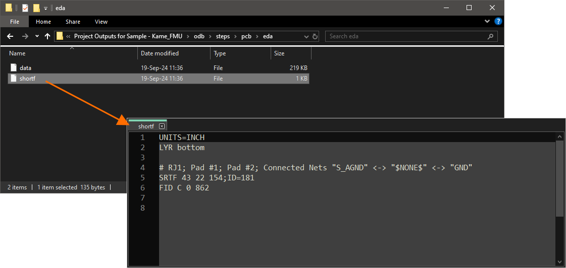 ).
).
Поддержка генерации файла shortf доступна, когда включена опция ODB.IntentionalShorts в диалоге Advanced Settings.
-
Support for mid-layer components – компоненты, размещённые на среднем слое (mid layer), включаются в экспорт. Это обеспечивается добавлением атрибута слоя размещения к данным слоя компонента в экспортируемых ODB++ файлах ( ).
).
Единицы измерения
Когда опция v. 8.1 выбрана в качестве ODB++ Version, выберите Millimeters или Inches в качестве предпочтительной единицы измерения. Когда опция v. 7.0 выбрана в качестве ODB++ Version, Inches выбираются по умолчанию и не могут быть изменены.
Параметры файлов
Установите флажок рядом с типом файла, который вы хотите использовать для генерации выходных файлов. Доступны варианты: несжатые, .zip и .tar/.tgz файлы.
Файл TGZ — это TAR-архив, сжатый с помощью GZIP. TAR-архив используется для объединения файлов, а сжатие GZIP — для уменьшения их размера; файлы TGZ меньше, чем обычные Zip-файлы. Поскольку TGZ предпочитают многие CAM-системы, например Frontline Genesis, файл TGZ может упростить процесс подготовки к производству.
Прочее
-
Include unconnected mid-layer pads – отметьте, чтобы разрешить несоединённые площадки на среднем слое (mid-layer) на ODB++ графиках.
-
Generate DRC Rules export file (.RUL) – отметьте, чтобы сгенерировать файл .RUL, содержащий все правила проектирования, определённые для исходного документа, из которого генерируются данные ODB++.
-
Export only the objects inside the board outline – отметьте, чтобы указать источник, который будет использоваться для создания слоя профиля ODB++. Слой профиля содержит внешнюю границу платы. По умолчанию это поле установлено в Board Outline (также называемое формой платы; это замкнутый многоугольник, определяющий границу, или габариты, печатной платы). Создаваемая при каждой новой плате, форма платы, вероятно, является лучшим источником для создания слоя Profile. Если в вашем проекте нет связанной формы платы, вы можете выбрать, какой исходный слой PCB использовался для определения замкнутого многоугольника, представляющего границу платы (например, слой KeepOut или конкретный Mechanical-слой). Эта опция доступна только когда исходный документ содержит встроенный объект массива плат (embedded board array), и она позволяет управлять областью объектов, экспортируемых. Обратите внимание: если объект (например, текст) находится вне контура платы, но касается его, и эта опция включена, такой объект всё равно будет экспортирован.
-
Merge Net-Tie Nets – если включено и проект содержит цепи, соединённые компонентами Net-Tie, эти цепи будут отображаться в нетлисте как различимые отдельные цепи. Обратите внимание: эта опция отключается, когда включена опция Generate shortf: List of Intentional Shorts (Net-Ties) .
-
Generate shortf: List of Intentional Shorts (Net-Ties) – при генерации выходных данных в формате ODB++ версии 8.1 (v. 8.1 выбрано в качестве ODB++ Version), включите, чтобы сгенерировать файл shortf, содержащий список цепей и медных примитивов, которым намеренно разрешено замыкаться («Net-Ties»). Сгенерированный файл можно найти в подпапке eda вывода шага (step output). Обратите внимание: эта опция отключается, когда включена опция Merge Net-Tie Nets .
-
Distinguish different footprints with the same name – если включено и один из посадочных мест (footprint) с одинаковым именем был изменён, в выходных данных изменяется только модифицированное посадочное место. Если опция не включена, все посадочные места с одинаковым именем будут отображаться как изменённые в выходных данных.
-
Generate Additional Tools by Drill Symbols – включите, чтобы генерировать дополнительные инструменты сверления на основе заданных группировок Drill Symbol. Будут добавлены дополнительные данные столбцов там, где они существуют в группировке Drill Symbols. Существующие столбцы данных не будут удалены из сгенерированных данных сверления.
-
Include Variants Data – при генерации выходных данных в формате ODB++ версии 8.1 (v. 8.1 выбрано в качестве ODB++ Version), включите, чтобы добавить информацию обо всех вариантах исполнения проекта (включая
[No Variations]). При включении этой опции в выходные данные включается следующая информация:
-
Состояние каждого компонента внутри любого экспортируемого варианта (установлен / не установлен).
-
Информация об альтернативной(ых) детали(ях) на уровне компонента для любого экспортируемого варианта.
-
Параметры каждого компонента в соответствии с вариацией.
-
Пользовательские параметры, применённые к каждому варианту/компоненту.
Когда эта опция отключена, выходные данные генерируются для варианта, выбранного в файле Outjob, или, когда вывод генерируется напрямую из редактора PCB (File » Fabrication Outputs » ODB++), для текущего активного варианта, выбранного на панели Projects.
-
Когда генерация ODB++ настраивается из файла Outjob и опция Include Variants Data включена, все варианты проекта включаются в вывод ODB++ независимо от того, какой вариант выбран для файла Outjob или для вывода.
-
Обратите внимание, что вариации для паяльных масок пасты не учитываются. Если вариации пастовой маски должны быть включены, убедитесь, что опция Allow Variation for Paste Mask включена в настройках требуемых вариантов, и генерируйте выходные данные для каждого варианта отдельно, при отключённой опции Include Variants Data в диалоге ODB++ Setup.
Слои для построения (Layers to Plot)
Установите флажок рядом с каждым конкретным слоем (слоями), который вы хотите построить как часть генерируемого вывода.
Нажмите кнопку , чтобы открыть диалог Add Mechanical Layers , в котором можно выбрать механические слои, добавляемые ко всем плотам или к выбранному плоту.
Диалог Add Mechanical Layers
Если проект включает переходные отверстия (vias) с назначенными типами IPC-4761, соответствующие механические слои (например, Filling, Capping и т. п.) будут перечислены в списке слоёв в группе слоёв IPC-4761 Via Type Features .
Слои построения (Plot Layers)
Используйте выпадающий список или щёлкните правой кнопкой мыши в разделе Layers to Plot, чтобы быстро выбрать группу слоёв для построения.
-
All On - нажмите, чтобы установить все флажки в столбце Plot (данные ODB++ будут созданы для всех отмеченных слоёв).
-
All Off - нажмите, чтобы снять все отмеченные флажки в столбце Plot (данные ODB++ создаваться не будут).
-
Used On - нажмите, чтобы установить все флажки в столбце Plot для слоёв, которые используются в проекте.
-
Edit Group - нажмите, чтобы открыть диалог Add Mechanical Layers , в котором можно выбрать механические слои, добавляемые к выбранному плоту. Также можно нажать , связанный с группой слоёв, или щёлкнуть правой кнопкой мыши по группе слоёв и затем выбрать Edit Group, чтобы открыть диалог Add Mechanical Layers .
Дополнительные параметры
Щелчок правой кнопкой мыши в разделе Custom Layers отобразит:
-
Add Layer - нажмите, чтобы добавить слой.
-
Edit Layer - нажмите, чтобы отредактировать слой.
-
Delete Layer - нажмите, чтобы удалить слой.
Щёлкните ячейку списка слоёв пользовательского слоя в разделе Custom Layers, чтобы открыть диалог Select Layer, в котором можно выбрать слои, добавляемые к выбранному пользовательскому слою.
Генерация из встроенного массива плат (Embedded Board Array)
При генерации вывода ODB++ из проекта PCB, содержащего встроенный массив плат, применимы следующие утверждения:
-
Проект автоматически анализируется на нарушения стека слоёв.
-
Встроенные платы, которые перевёрнуты, будут отображать свои стеки слоёв как перевёрнутые.
-
Различающиеся средние сигнальные слои и внутренние полигоны питания (internal planes) всё равно могут отображаться на одной и той же панели среднего слоя.
-
Средние сигнальные слои и внутренние полигоны питания могут быть перевёрнуты относительно друг друга.
При генерации вывода ODB++ из проекта PCB будут экспортированы все объекты на всех слоях, включённых для построения. Если вы хотите экспортировать только объекты проекта, находящиеся внутри контура платы, убедитесь, что все дополнительные слои, содержащие объекты за пределами этой границы, отключены для построения.
Расположение сгенерированных файлов ODB++
Путь вывода для сгенерированных файлов зависит от того, как был сформирован вывод:
- Из файла OutputJob — сгенерированные файлы сохраняются в папке внутри папки проекта. Именование и структура папок задаются в Output Container, на который нацелен вывод ODB++.
-
Непосредственно из PCB — путь вывода задается в диалоге Project Options - Options dialog. По умолчанию путь вывода указывает на подпапку внутри папки, содержащей файл проекта, и имеет имя
Project Outputs for <ProjectName>. При необходимости путь вывода можно изменить. Если на вкладке Options включена опция использования отдельной папки для каждого типа вывода, то файлы ODB++ будут записываться в дополнительную подпапку с именем ODB++ Output.
Автоматическое открытие сгенерированного вывода ODB++
При генерации вывода ODB++ можно указать, чтобы результат автоматически открывался в новом CAM-документе. Способ выполнения зависит от того, как вы генерируете вывод:
-
Из файла OutputJob — включите опцию автозагрузки ODB++ Output в диалоге Output Job Options (Tools » Output Job Options из OutputJob Editor).
-
Непосредственно из PCB — убедитесь, что опция Open outputs after compile включена на вкладке Options диалога Project Options (Project » Project Options).
Генерация производственных данных IPC-2581
Связанный с существующим форматом ODB++, IPC-2581 — это стандарт с открытой спецификацией, разработанный Institute for Printed Circuits IPC-2581 Consortium в 2004 году, а затем доработанный до последних выпусков Revision A и B (IPC-2581A/B).
Стандарт постепенно получил более широкое признание как альтернатива традиционным производственным выходным данным, которые обычно представляют собой набор файлов Gerber, Drill, BOM, текстовых файлов и т. п. Прежняя необходимость в сложной смеси производственных файлов обусловлена присущими ограничениями традиционного формата Gerber RS-274x, в котором отсутствуют определения стека слоев, информация о сверлении, данные нетлиста (электрическая связность) и сведения BOM.
Официальное название стандарта IPC-2581 — «Generic Requirements for Printed Board Assembly Products Manufacturing Description Data and Transfer Methodology», и он предлагает единый формат файла на основе XML, включающий широкий набор данных для изготовления платы — от сведений о стеке слоев до полной информации о площадках/трассировке/компонентах и ведомости материалов (BOM).
Один XML-файл IPC-2581 может включать:
-
Информацию об изображении меди для травления слоев PCB.
-
Информацию о стеке слоев платы (включая жесткие и гибкие участки).
-
Нетлист для тестирования голой платы и внутрисхемного тестирования.
-
Ведомость материалов компонентов для закупки и сборки (pick-and-place).
-
Примечания и параметры для изготовления и сборки.
Потенциальное преимущество применения формата IPC-2581 для передачи данных проектирования платы на производство и сборку заключается в строго определенном, детализированном формате единого файла, который однозначно понимается на обоих концах цепочки. При налаженном обмене данными CAD–CAM риски, связанные с неверной интерпретацией данных, ошибками файлов и вариативностью трактовки Gerber, в значительной степени устраняются. Иными словами, форматы IPC-2581 и Gerber X2 представляют новое поколение передачи данных «проектирование → производство».
Чтобы получить доступ к функциональности IPC-2581 в Altium Designer, необходимо установить IPC2581 расширение ПО. По умолчанию это расширение устанавливается вместе с Altium Designer. Его можно установить или удалить вручную.
Дополнительные сведения об управлении расширениями см. на странице Extending Your Installation (Altium Designer Develop, Altium Designer Agile, Altium Designer).
Когда PCB-файл проекта загружен как активный документ, файл IPC-2581 можно сгенерировать, выбрав File » Fabrication Outputs » IPC-2581 в главном меню. Откроется начальный диалог IPC-2581 Configuration, в котором можно указать используемую редакцию стандарта IPC-2581 (A или B), а также единицы измерения и точность чисел с плавающей запятой, применяемую в процессе экспорта.

Задайте параметры экспорта в диалоге IPC-2581 Configuration.
Options and Controls of the IPC-2581 Configuration Dialog
-
IPC2581 version — используйте выпадающий список, чтобы выбрать корректную версию IPC-2581.
-
Measurement System — используйте выпадающий список, чтобы выбрать единицы Metric или Imperial .
-
Floating Point Precision — введите нужное значение или используйте клавиши со стрелками, чтобы выбрать требуемую точность чисел с плавающей запятой.
-
OEMDesignNumberRef — используйте выпадающий список, чтобы выбрать используемый параметр компонента. DesignItemID используется по умолчанию.
-
Merge Net-Tie Nets — если включено, и в проекте есть цепи, соединенные компонентами Net-Tie, эти цепи будут отображаться в нетлисте как различимые отдельные цепи.
-
Distinguish different footprints with the same name — если включено, и один из посадочных мест с одинаковым именем был изменен, в выходных данных будет изменено только модифицированное посадочное место. Если опция отключена, все посадочные места с одинаковым именем будут показаны как измененные в выходных данных.
Настройка точности определяет позиционную точность и точность размеров данных в сгенерированном файле, соответствующем IPC-2581, как показано на изображении ниже.
 и 6 (справа).")
Один и тот же фрагмент файла IPC-2581 при точности 2 (слева) и 6 (справа).
XML-файл IPC-2581 будет экспортирован в расположение, заданное в поле Output Path на вкладке Options tab of the Project Options dialog. Имя будет сформировано по шаблону <PCBDocumentName>.cvg.
Сгенерированный файл будет добавлен в проект и появится в панели
Projects panel в папке
Generated\Text Documents.
Генерация производственных данных NC Drill
Файлы сверления используются в процессе изготовления платы для сверления отверстий в PCB. Параметры вывода NC Drill настраиваются в диалоге NC Drill Setup.

Диалог NC Drill Setup
Диалог NC Drill Setup открывается одним из следующих способов:
-
С помощью генератора вывода NC Drill в файле конфигурации OutputJob (*.OutJob). Вывод генерируется при запуске настроенного генератора.
-
В активном документе PCB нажмите File » Fabrication Outputs » NC Drill Files. Вывод будет сгенерирован сразу после нажатия OK в диалоге.
Параметры, заданные в диалоге NC Drill Setup при генерации вывода непосредственно из PCB, отличаются и отделены от параметров, заданных для того же типа вывода в файле конфигурации OutputJob. В первом случае параметры сохраняются в файле проекта, во втором — в файле конфигурации OutputJob.
Options and Controls of the NC Drill Setup Dialog
-
NC Drill Format — используйте эту область, чтобы задать единицы измерения и формат, используемые в выходных файлах NC Drill.
-
Units
-
Inches — включите эту опцию, чтобы использовать дюймовые единицы, где вся работа ведется в милах (1/1000 дюйма).
-
Millimeters — включите эту опцию, чтобы использовать метрические единицы, где вся работа ведется в миллиметрах.
-
Format
-
2:3/4:2 — обеспечивает разрешение 1 mil/0,01 мм.
-
2:4/4:3 — обеспечивает разрешение 0,1 mil/1 мкм.
-
2:5/4:4 — обеспечивает разрешение 0,01 mil/0,1 мкм.
Отображаемые форматы зависят от выбранного Units, что также отражается на разрешении. Различные форматы и разрешения приведены выше.
Если вы используете одно из более высоких разрешений, проверьте, поддерживает ли производитель PCB этот формат. Форматы 4:3 и 4:4 следует выбирать только в том случае, если на плате есть отверстия на сетке с шагом меньше 1 mil.
-
Leading/Trailing Zeroes — подавление нулей — это метод уменьшения размера генерируемых файлов данных путем удаления всех нулей в начале (leading) или в конце (trailing) чисел.
-
Keep leading and trailing zeroes– если этот параметр включен, в сгенерированном файле NC Drill будут присутствовать все ведущие и завершающие нули.
-
Suppress leading zeroes – если этот параметр включен, в сгенерированном файле NC Drill не будут отображаться ведущие нули.
-
Suppress trailing zeroes – если этот параметр включен, в сгенерированном файле NC Drill не будут отображаться завершающие нули.
-
Coordinate Positions
-
Reference to absolute origin – использовать абсолютное начало координат в качестве опорной точки.
-
Reference to relative origin – использовать относительное начало координат в качестве опорной точки.
-
Other
-
Optimize change location commands – включите этот параметр, чтобы оптимизировать любые команды смены позиции.
-
Generate separate NC Drill files for plated & non-plated holes – включите этот параметр, чтобы создавать отдельные файлы сверловки для металлизированных и неметаллизированных отверстий.
-
Generate separate NC Drill files for VIA features – включите этот параметр, чтобы создавать отдельные файлы сверловки для каждого типа переходных отверстий по IPC 4761.
-
Use drilled slot command (G85) – включите этот параметр, чтобы использовать несколько просверленных отверстий для формирования пазов.
-
Generate Board Edge Rout Paths – включите этот параметр, чтобы создать отдельный файл NC Rout для задания контура платы, включая вырезы в плате.
-
Generate EIA Binary Drill File (.DRL) – используйте этот параметр для генерации файла .DRL. DRL — это двоичный формат файла сверловки. Для многослойной печатной платы со слепыми и/или скрытыми переходными отверстиями создается отдельный файл сверловки для каждой пары слоев с уникальным расширением файла.
-
Generate Additional Tools by Drill Symbols - включите, чтобы генерировать дополнительные инструменты сверления на основе заданных группировок Drill Symbol. Будут добавлены дополнительные данные столбцов там, где они существуют в группировке Drill Symbols. Существующие столбцы данных не будут удалены из сгенерированных данных сверловки.
Файлы NC Drill следует создавать в том же формате, что и файлы Gerber. В противном случае координаты сверления могут не совпасть с координатами площадок/переходных отверстий. Например, если файлы Gerber настроены на использование формата 4:3, то соответствующие файлы NC Drill должны использовать тот же формат. Если файлы Gerber были сгенерированы с настройкой позиции координат на пленке с использованием абсолютного или относительного начала координат, то файлы NC Drill в идеале следует генерировать с тем же опорным началом координат.
Сгенерированные файлы NC Drill
| Filename |
Description |
| FileName.DRL |
Двоичный формат файла сверловки. Для многослойной печатной платы со слепыми и/или скрытыми переходными отверстиями создается отдельный файл сверловки для каждой пары слоев с уникальным расширением файла. |
| FileName.DRR |
Отчет по сверлению — содержит назначение инструментов, размеры отверстий, количество отверстий и перемещения инструмента. |
| FileName.TXT |
ASCII-формат файла сверловки. Для многослойной печатной платы со слепыми и/или скрытыми переходными отверстиями создается отдельный файл сверловки для каждой пары слоев с уникальным расширением файла. |
| FileName-Plated.TXT |
ASCII-формат файла сверловки. Предназначен специально для металлизированных отверстий в проекте печатной платы. Для каждого типа отверстий — пазовых, квадратных или круглых — будет создан отдельный файл. |
| FileName-NonPlated.TXT |
ASCII-формат файла сверловки. Предназначен специально для неметаллизированных отверстий в проекте печатной платы. Для каждого типа отверстий — пазовых, квадратных или круглых — будет создан отдельный файл. |
| FileName-BoardEdgeRout.TXT |
ASCII-формат файла фрезеровки. Предназначен специально для контура платы, включая вырезы в плате. |
| FileName.LDP |
ASCII-формат отчета по парам сверления. Используется CAM Editor для обнаружения слепых и скрытых переходных отверстий. |
После генерации выходные файлы будут добавлены в проект и появятся в панели Projects в папке Generated в соответствующим образом названной подпапке. Если вы использовали отдельную папку для каждого типа выходных данных, то соответствующие (отдельные) папки Generated будут добавлены в панель Projects (например, Generated (NC Drill Output)).
Расположение сгенерированных файлов NC Drill
Путь вывода для сгенерированных файлов зависит от того, как был сформирован вывод:
-
Из файла OutputJob — сгенерированные файлы сохраняются в папке внутри папки проекта. Имена и структура папок задаются в Output Container, на который нацелен вывод NC Drill File.
-
Непосредственно из PCB — путь вывода задается в диалоге Project Options – Options. По умолчанию путь вывода установлен в подпапку внутри папки, содержащей файл проекта, и имеет имя Project Outputs for <ProjectName>. При необходимости путь вывода можно изменить. Если на вкладке Options включен параметр использования отдельной папки для каждого типа выходных данных, файлы NC Drill будут записаны в дополнительную подпапку с именем NC Drill Output.
Автоматическое открытие сгенерированного вывода NC Drill
При генерации выходных данных NC Drill можно указать, чтобы результат автоматически открывался в новом CAM-документе. Способ выполнения зависит от того, как вы генерируете вывод:
-
Из файла OutputJob — включите параметр автозагрузки NC Drill Output в диалоге Output Job Options (Tools » Output Job Options из OutputJob Editor).
-
Непосредственно из PCB — убедитесь, что параметр Open outputs after compile включен на вкладке Options диалога Project Options (Project » Project Options).
Формирование отчета по стеку платы
Altium Designer поддерживает создание Board Stack Report в формате Excel (<PCBDocumentName>.xls), который суммирует заданные стеки слоев и слои, используемые в stackup (в терминах имени слоя, материала, толщины и диэлектрической проницаемости). Также суммируется высота каждого стека. Параметры вывода Board Stack Report настраиваются в диалоге Layer Stack Report Setup, где можно указать единицы измерения и столбцы, которые нужно отображать в отчете.

Диалог Layer Stack Report Setup
Описанный выше диалог Layer Stack Report Setup доступен, когда параметр PCB.ModernBoardStackGenerator включен в диалоге Advanced Settings. Когда этот параметр отключен, доступен диалог Layer Stack Report Setup, в котором можно указать только единицы измерения в отчете ( ).
).
Формирование производственных данных на основе печати
Следующие выходные данные являются печатными (print-based) выходами с предопределенными настройками страниц и слоев на них:
-
Composite Drill Guide - формирует предопределенный сводный чертеж сверловки для исходного PCB-документа.
-
Drill Drawings - формирует предопределенный набор чертежей сверловки и направляющих для исходного PCB-документа.
-
Final - формирует полный, предопределенный финальный набор печатных материалов (artwork print-set) для исходного PCB-документа.
-
Mask Set - формирует предопределенные чертежи паяльной/пастовой маски для исходного PCB-документа.
-
Power-Plane Set - формирует предопределенные чертежи силовых полигонов (power-plane) для исходного PCB-документа.
Откройте диалог Print, чтобы просмотреть и скорректировать конфигурацию вывода.
Подробнее см. на странице Configuring PCB Printouts.
Формирование отчета по производственным тестпоинтам
Генератор отчета по производственным тестпоинтам формирует отчет (в форматах txt и/или csv и/или IPC-D-356A) по всем площадкам и переходным отверстиям, настроенным для использования в качестве производственных тестпоинтов.
Подробнее о назначении тестпоинтов в проекте печатной платы см. на странице Assigning Testpoints on the Board.
Отчет по тестпоинтам поддерживает встроенные массивы плат (embedded board arrays). При экспорте из PCB-документа, содержащего несколько встроенных массивов плат, формируется несколько netlist-файлов IPC-D-356A.
Параметры вывода Fabrication Testpoint Report настраиваются в диалоге Fabrication Testpoint Setup.

Диалог Fabrication Testpoint Setup
Отчет по производственным тестпоинтам использует только настройки тестпоинтов для площадок и переходных отверстий
Fabrication , тогда как
отчет по сборочным тестпоинтам использует только настройки тестпоинтов
Assembly . Обратите внимание: диалог
Assembly Testpoint Setup, используемый для настройки Assembly Fabrication Report, имеет тот же набор параметров, что и диалог
Fabrication Report Setup.
Options and Controls of the Testpoint Setup Dialog
Форматы отчета
-
Text - включите для стандартного текстового формата в отчете.
-
CSV - включите для стандартного формата CSV (значения, разделенные запятыми), который можно импортировать в табличное приложение, например Excel, для дальнейшей обработки.
-
IPC-D-356A - включите для IPC netlist-файла, который содержит информацию о слепых и скрытых переходных отверстиях, а также различает сквозные переходные отверстия и свободные площадки. При импорте в CAM-документ вместе с данными изображений и сверловки это облегчает восстановление исходных имен цепей, использованных в проекте печатной платы, делая плату более понятной и удобной для работы в CAM Editor.
Слои тестпоинтов
Эти параметры позволяют задать область охвата отчета:
-
Top layer - отметьте, чтобы включить корректные тестпоинты, назначенные на верхней стороне платы.
-
Bottom layer - отметьте, чтобы включить корректные тестпоинты, назначенные на нижней стороне платы.
Единицы измерения
-
Imperial- отметьте, чтобы выводить координаты в дюймах.
-
Metric - отметьте, чтобы выводить координаты в миллиметрах.
Позиции координат
-
Reference to absolute origin - выберите, чтобы использовать абсолютное начало координат в качестве опорной точки для координат тестпоинтов.
-
Reference to relative origin - выберите, чтобы использовать относительное начало координат в качестве опорной точки для координат тестпоинтов.
Параметры IPC-D-356A
Этот раздел диалога становится доступен только когда включен параметр IPC-D-356A Report Format .
-
Adjacency Information - отметьте, чтобы включить список цепей, которые потенциально могут быть закорочены, затем введите критерии смежности в текстовое поле.
-
Board Outline- установите флажок, чтобы разрешить описание контуров и других данных сегментного типа, которые не привязаны к конкретной цепи (net), затем используйте раскрывающийся список, чтобы выбрать нужные данные.
-
Conductor Traces - Подробнее см. спецификацию IPC-D-356A.
-
Merge Net-Tie Nets - если включено, и проект содержит цепи, соединённые компонентами Net-Tie, эти цепи будут отображаться в нетлисте как различимые отдельные цепи.
Сгенерированные файлы отчётов для производства
Все сгенерированные файлы тестпоинтов сначала именуются по типу (Fabrication или Assembly), затем по имени файла. Например: Fabrication Testpoint Report for BoardFileName. В зависимости от того, какой из параметров Report Formats включён, используются следующие расширения файлов: .txt, .CSV, .IPC (обратите внимание, что это ASCII-файл).
Расположение сгенерированных файлов отчётов для производства
Путь вывода для сгенерированных файлов зависит от того, как был сформирован вывод:
-
Из файла OutputJob — сгенерированные файлы сохраняются в папке внутри папки проекта. Именование и структура папок задаются в Output Container, на который нацелен вывод Testpoint.
-
Непосредственно из PCB — путь вывода задаётся в диалоге Project Options - Options dialog. По умолчанию путь вывода указывает на подпапку внутри папки, содержащей файл Project, и имеет имя:
Project Outputs for ProjectName. При необходимости путь вывода можно изменить. Если на вкладке Options включена опция использования отдельной папки для каждого типа вывода, то файлы Testpoint будут записаны в дополнительную подпапку с именем Testpoint Output.
Автоматическое открытие сгенерированного вывода отчёта для производства
При генерации вывода Testpoint можно указать, чтобы результат автоматически открывался в новом CAM-документе. Способ выполнения зависит от того, как вы формируете вывод:
-
Из файла OutputJob — включите опцию автозагрузки IPC-D-356A Output в диалоге Output Job Options (Tools » Output Job Options из редактора OutputJob Editor).
-
Непосредственно из PCB — убедитесь, что опция Open outputs after compile включена на вкладке Options диалога Project Options (Project » Project Options).
Вывод производственных файлов через файл Output Job
Чтобы включить вывод производственных файлов в Output Job Configuration file проекта, нажмите [Add New Fabrication Output] в разделе Fabrication Outputs, затем выберите тип вывода в меню и нужный источник данных в соответствующем подменю.
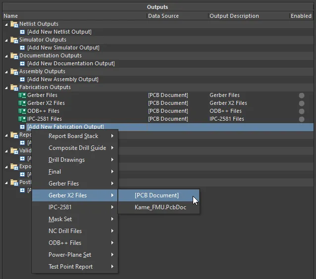
Настройте производственные выводы как часть Fabrication Outputs файла Output Job. Здесь показан пример для Gerber X2 файлов.
Когда OutJob запускается — вручную или в рамках project release process — производственные выводы будут сгенерированы в соответствии с настройками, заданными для соответствующего Output Container.

Подготовка производственных выводов как часть настроенного OutJob.
Настройки, задаваемые в связанных диалогах при генерации производственных выводов непосредственно из PCB, отличаются и отделены от настроек, определённых для того же типа вывода в файле OutputJob Configuration. В первом случае настройки сохраняются в файле проекта, тогда как во втором — в файле OutputJob Configuration.

 Локализовано с помощью ИИ