従来、PCBは2次元の設計空間でレイアウトされ、PCBの各層は色で表現されてきました。しかし、実際のPCBは3次元の物体であるため、PCB設計者は画面上の多層2D表現を、頭の中で3D表現へと対応付ける必要がありました。
3Dビデオカードとそれを支えるソフトウェア技術の大幅な進歩により、Altiumはこの問題に対する解決策、すなわち真の3次元PCB編集を開発できるようになりました。単なる可視化にとどまらず、Altium Designerの3D機能により次のことが可能になります。
-
3Dクリアランスチェックの実行 - 必要に応じて、部品同士や筐体に対して部品を厳密に位置合わせできます。
-
保守のためにアクセスが必要なコネクタやその他の部品を視覚的に特定できます。
-
すべての機械的制約が考慮されていることを把握したうえで、製造プロセスや組立順序をより明確に定義できます。
-
人が実際に目にするものにより近い画像を用いて、手組み手順書、ユーザーマニュアル、作業指示書をより詳細に作成できます。
-
筐体や周辺環境と調和し、より見栄えの良い製品にするために、異なる色のソルダーマスクを試せます。
-
最終製品のより具体的な見え方を提示することで、主要な関係者の合意を得やすくなります。

同一領域のボードの2D表示と3D表示。
表示モード
Altium Designerは、ボードを2Dまたは3Dで表示・編集することをサポートしており、これらは display modesと呼ばれます。必要なモードはViewメニューで選択するか、 1、 2 または 3 のショートカットで、そのモードへ直接切り替えます。
表示モードは3種類あり、それぞれ固有の機能があります。
-
Board Planning Mode (ショートカットキー 1) - ボード形状の定義に使用し、リジッドフレックス設計におけるスプリットラインおよびベンディングラインの配置と設定にも使用します。スプリットラインはボードを領域に分割するために使用され、各領域には異なるレイヤースタックを割り当てられます。ボード領域およびスプリットライン/ベンディングラインの詳細は、Defining the Layer Stackを参照してください。
-
2D Layout Mode (ショートカットキー 2) - 従来の2Dの多層表示です。Altium Designerには、ボードの表示管理を支援するBoard Insight Systemと呼ばれる一連の機能が組み込まれています。
-
3D Layout Mode (ショートカットキー 3) - 真の3D設計です。3D表示モードを3Dマウスと組み合わせることで、読み込まれた 3Dボード を、手に持っているかのように表示・操作できます。PCBの3D表示の操作方法の詳細は、Controlling the 3D Viewページを参照してください。
3D Layout Mode には、DirectX 9以降およびShader Model 3以降に対応したグラフィックスカードが必要です。
 同じボードを、Board Planningモード、2D Layoutモード、3D Layoutモードで表示した例。
View Configuration Panel
PCBエディタの設計空間に現在表示されている内容と、その表示方法は、View Configurationパネルで設定できます。これには、レイヤーの表示/非表示と色、オブジェクトの表示/非表示と透明度、マスキングとディミングのレベル、現在の単一レイヤーモード、さらにパッド/ビア/配線上のネット名表示など、設計空間の表示に関する追加機能が含まれます。

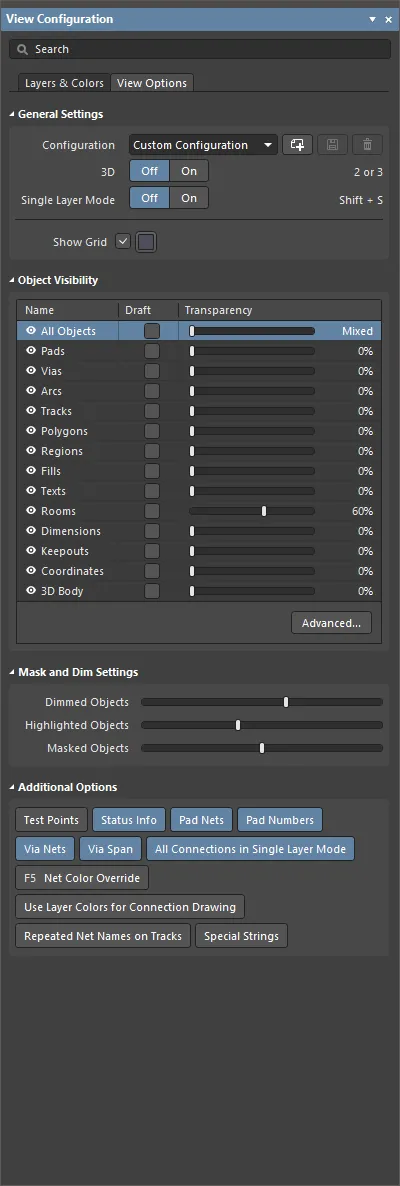
表示に関する設定はView Configurationパネルで行います。
パネルへの標準的なアクセス方法(設計空間右下の Panels ボタン、または View » Panels メニュー)に加えて、View ConfigurationパネルはLまたは Ctrl+Dのショートカットキーでも開けます(それぞれ Layers & Colorsタブ、または View Optionsタブを表示した状態でパネルを開く)。また、設計空間左下のLayer Setsコントロールにある色見本( )をクリックしてアクセスすることもできます。
パネル内容は2つのタブに分かれています。パネル上部のタブをクリックすると、そのタブで利用可能なオプションが表示されます。
利用可能なオプションは、現在のLayout Mode(2Dまたは3D)によって異なります。
3D Layoutモードでは、
View Configurationパネルに
Section Viewタブも表示されます。このタブを使用してPCBの断面表示を設定します –
learn more。
レイヤー表示の設定
各レイヤーは、View ConfigurationパネルのLayers & Colorsタブ内にあるLayers領域から表示/非表示を切り替えられます。表示アイコン( )をクリックして、表示/非表示を切り替えます。

表示アイコンでレイヤーの表示状態を管理
該当する場合、各グループにも表示アイコンがあります。たとえば上の画像では次のとおりです。
-
文字列Component Layer Pairs (C) の左にある表示アイコンは、allのコンポーネントレイヤーの表示/非表示を切り替えます。
-
文字列Top の左にある表示アイコンは、all top sideのコンポーネントレイヤーの表示/非表示を切り替えます。Bottom側のレイヤーも同様に表示/非表示を切り替えられます。
Controlling Layer Visibility from the Keyboard
要素の多いPCB設計では、設計中にレイヤーの表示/非表示を頻繁に切り替えることがあります。これを支援するため、レイヤーの表示状態は次の方法でキーストロークにより変更できます。
-
Lショートカットキーを押して、View ConfigurationパネルのLayers & Colorsタブを表示/アクティブにします。パネルのタイトルバーが色付きになり、ソフトウェア内でアクティブ要素であることが示されます。
-
一部のレイヤーやレイヤーセットの右側には、丸括弧内に文字や数字が表示されています。例: Component Layer Pairs (C)、[1] Top (T)。この丸括弧内の文字/数字がキーボードショートカットです。例として、Lショートカットでパネルをアクティブにし、その後Tショートカットを押すと、Top信号レイヤーの表示/非表示が切り替わります。
-
レイヤーセットにアクセスしている場合、Spacebarを押すと、そのセット内のすべてのレイヤーの表示/非表示が切り替わります。
-
レイヤーにアクセスしている場合、その表示状態は即座に切り替わり、続けてSpacebarを使って再度切り替えられます。
-
UpまたはDownの矢印キーでリストを上下に移動できます。たとえば特定のメカニカルレイヤーやコンポーネントレイヤーペアにアクセスし、その後Spacebarでそのレイヤー/レイヤーペアの表示/非表示を切り替えられます。
-
角括弧内の数字は、そのSignalレイヤーまたはPlaneレイヤーがレイヤースタック内で何番目の物理銅層であるかを示します。文字列[6] Bottom (B)を例にすると、[6]はレイヤースタック内で6番目の銅層であることを示し、BottomはLayer Stack Managerでユーザーが割り当てたレイヤー名、(B)はそのレイヤーの表示/非表示を切り替えるショートカットキーです。
-
SignalレイヤーおよびPlaneレイヤーのショートカットキーは、キーボード上で最後に利用可能な数字キーである(9)までです。
レイヤーセット
Layer Set は、表示するレイヤーをまとめた「名前付きのレイヤーセット」です。既存の Layer Set を選択するには、View Configuration パネルの Layers & Colors タブにある Layers 領域の Layers Sets ドロップダウンを使用します。表示は更新され、その Layer Set で有効になっているレイヤーのみが表示されます。ユーザー定義の Layer Set はいくつでも作成でき、現在選択中の Layer Set は編集することもできます。
-
新しいユーザー定義 Layer Set を作成するには、Layers 領域で必要に応じてレイヤーの表示/非表示を設定し、次に
 ボタンをクリックします。セットはドロップダウンに My Layers として表示されます。以降に追加する Layer Set には番号が付与されます。
-
既存のユーザー定義 Layer Set の有効レイヤー構成を変更するには、Layers Sets ドロップダウンで対象を選択し、必要に応じてレイヤーの表示/非表示を設定してから、
 ボタンをクリックして変更を Layer Set に保存します。
-
既存のユーザー定義 Layer Set の名前を変更するには、Layers Sets ドロップダウンで対象を選択し、Layer Sets フィールドに必要な名前を入力します。Layer Set の名前変更は保存操作を必要とせず、新しい名前は自動的に保存されます。
-
既存のユーザー定義 Layer Set を削除するには、Layers Sets ドロップダウンで対象を選択し、
 ボタンをクリックします。
-
PCB Layer Set File
(*.layerset) から目的の Layer Set をインポートする、または目的の Layer Set を PCB Layer Set File としてエクスポートするには、それぞれ Import ボタンと Export ボタンを使用します。
表示する Layer Set を切り替えるには、次の方法を使用します:
-
Layer SetView Configuration パネルのドロップダウン
-
Design » Manage Layer Sets サブメニュー
-
Layer Set コントロール - デザインスペース下部のレイヤータブ左側にあるボタンの LS 部分をクリックしてアクセスします(
 )。
)。
System Colors
System Colors 領域では、リストにある項目について PCB 上で使用される色を設定できます。色と表示/非表示は通常の手順で設定します。
Layer Tabs
View Configuration パネルで現在「表示」に設定されている各レイヤーに対応するタブは、デザインスペースの下端に配置されています。

これらのタブにより、アクティブレイヤー(オブジェクトを配置するレイヤー)を切り替えられるほか、現在表示されているレイヤーとアクティブレイヤー(ハイライトされたタブ)を視覚的に確認できます。一度に表示できるレイヤータブ数を超える場合は、矢印  を使用してタブをスクロールします。
レイヤー色はレイヤータブの左側に表示され、レイヤー色をダブルクリックすると Choose Color ダイアログが起動します。
レイヤー名をダブルクリックすると Edit Layer ダイアログが開き、そこでレイヤー名(および internal plane layer の場合はネット名)を編集できます。

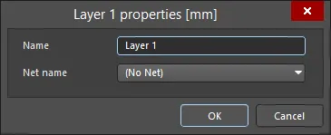
Edit Layer ダイアログ
Single-Layer Mode
Single-Layer 2D Display Mode
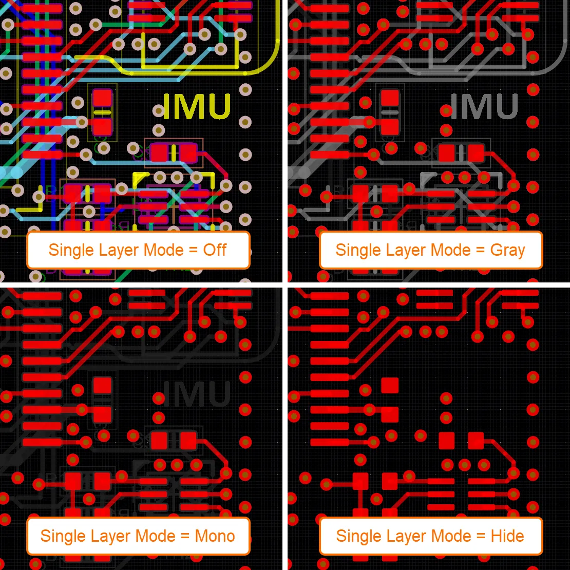
Board Insight に統合されている Single-Layer モード機能は、Preferences ダイアログの PCB Editor - Board Insight Display ページで設定します。Single Layer モードは、現在のレイヤーの内容を表示しつつ、他のすべてのレイヤーの内容を非表示または減光します。現在のレイヤー内容のみを表示するために他レイヤー上のすべてのオブジェクトを非表示にするだけでなく、Single-Layer モードにはグレースケール表示およびモノクロ表示モードもあります。他レイヤーの色をすべてグレースケールまたはモノクロに変換することで、注目しているレイヤーの作業を妨げることなく、設計内の他オブジェクト位置に関する空間的な関係情報を保持できます。フル表示と有効化されている各 Single-Layer モードを順に切り替えるには、Shift+S ショートカットを押します。Shift+S を押すたびに、ソフトウェアは次の有効モードへ移動し、最終的にフル表示モードへ戻ります。Single-layer モードは Preferences ダイアログの PCB Editor - Board Insight Display ページで有効化します。Shift+S を押したときに含めたくないモードは無効(チェックを外す)にしてください。これらの設定は、この Altium Designer インストール環境内のすべてのデザインに適用されます。
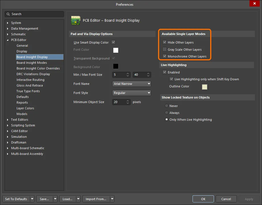
利用可能な single-layer モードは次のとおりです:
-
Hide Other Layers - 他のすべてのレイヤーを非表示にし、アクティブ(現在)レイヤーの内容のみを表示します。
-
Gray Scale Other Layers - 他のすべてのレイヤーを、現在のレイヤー色から導出したグレーの濃淡で表示し、アクティブレイヤーは標準色で表示します。
-
Monochrome Other Layers - 他のすべてのレイヤーを同一のグレーの濃淡で表示し、アクティブレイヤーは標準色で表示します。
以下の画像は、通常のマルチレイヤー表示と 3 つの single-layer 表示モードを示しています。
現在選択されている single-layer モードは、View Configuration パネルの View Options タブにある General Settings 領域に表示されます。モードリンク(On button の隣)をクリックすると、Preferences ダイアログの PCB Editor - Board Insight Display ページにアクセスでき、必要に応じて利用可能な single-layer モードを設定できます。
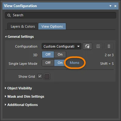
Gray または Mono の Single Layer モードにおける他レイヤーの明るさは、View Configuration パネルの View Options タブにある Mask and Dim Settings 領域の Masked Objects スライダーで調整します。
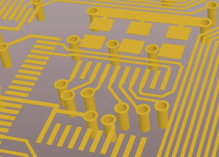
Single-Layer 3D Display Mode
single-layer モードは、ボードを 3D Layout Mode で表示している場合にも利用できます。特定レイヤーの配線品質や、電源プレーンレイヤーの品質を確認する、といった作業に使用します。single-layer モード中は、Ctrl+Shift+Wheel Roll ショートカットを使用してレイヤーを順に切り替えます。
Single Layer Mode 表示でレイヤーを常時表示する
Single Layer Mode 表示にレイヤーを含めるには、View Configuration パネルの Layers & Colors タブで目的のレイヤーに関連付けられた目のアイコンに対して Ctrl+Click を実行し、そのレイヤーを Single Layer Mode 表示に追加します。目のアイコンの背後に四角が表示され( )、そのレイヤーが Single Layer Mode で常時表示されることを示します。
ボードを下面側から表示する
ボードを下面側から表示する(実質的にボードを反転する)には、View Configuration パネルの Layers & Colors タブにある Layers 領域で View From Bottom Side オプションを有効にし、メインメニューから View » Flip Board コマンドを選択するか、Ctrl+F キーボードショートカットを使用します。
反転したボード/コンポーネントでも、すべての操作および編集コマンドがサポートされます。座標空間は論理的には同一のままで、つまりデザインスペースの原点は左下から右下へ移動します。現在のグリッド位置は、通常の左から右ではなく、マウスを右から左へ動かすと X(水平)方向に増加します。表示を反転した状態で生成される出力は、正しい「上面から見た」座標情報を維持します。
ボード/コンポーネントを反転すると、レイヤーの描画順も論理的なペア入れ替え処理によって変更されます。つまり、現在のレイヤー描画順において Top Overlay は Bottom Overlay と、Top Layer は Bottom Layer と、Mid-Layer 1 は Mid-Layer 30 と、Internal Plane 1 は Internal Plane 16 と…のように位置が入れ替わります。メカニカルレイヤーの描画順は変更されません。
オブジェクトの表示/非表示を制御する
レイヤーのオン/オフ切り替えによってデザインスペース内のオブジェクト表示を制御するだけでなく、オブジェクトタイプに基づいてオブジェクトの可視性と透明度を制御する方法もあります。2D Layout モードでは、View Configuration パネルの View Options タブにある Object Visibility 領域のオプションを使用して、タイプ別にオブジェクトの可視性と透明度を設定します。

パネルの View Options タブにある Object Visibility セクション:
-
– 該当する可視性アイコンをクリックして、特定のオブジェクトタイプの表示/非表示を制御します。All Objects 可視性アイコンをクリックすると、すべてのオブジェクトの表示/非表示を切り替えられ、その後に特定のオブジェクトタイプの表示を有効化できます。
-
Name – 視覚的に調整可能なすべてのオブジェクトを一覧表示します。
-
Draft – 有効にすると、オブジェクトタイプをアウトライン表示します。
-
Transparency – スライダーバーでそのオブジェクトタイプの透明度を調整するか、値をクリックして 0~100 の範囲で希望の割合を手入力します(0% は完全表示(不透明)、100% は完全透明(不可視))。オブジェクトを透明に設定すると、たとえばトラックセグメントの端がパッドに接する箇所など、あるオブジェクトが別のオブジェクトを覆っている状況を確認できます。
-
Advanced – クリックすると Object Visibility ダイアログが開き、異なるレイヤーにまたがる特定オブジェクトの共通透明度レベルを設定したり、特定レイヤー上の異なるオブジェクトに対して別々の透明度を設定したりできます。
このパネルの General Settings 領域で Custom Configuration を作成すると、好みの可視性設定を簡単に復元できます。
Mask and Dim Settings
単純なPCB設計であっても多数のオブジェクトが存在し得るため、それらの表示管理を支援する目的で、PCBエディタには関心のないオブジェクトをフェード表示できる機能があります。たとえば、PCBパネルのNetsモードでネットをクリックし、パネルのドロップダウンがDimまたはMaskに設定されている場合、そのネットに属さないすべてのオブジェクトがフェード表示されます。これにより、ネット やネットクラス、コンポーネントクラス、特定のデザインルールの対象となるオブジェクトなど、特定の設計要素により容易に注意を集中できます。マスキングおよびディミングのレベルは、View ConfigurationパネルのView OptionsタブにあるMask and Dim Settings 領域のスライダーで設定します。

View ConfigurationパネルのView OptionsタブにあるMask and Dim Settings領域
構成の管理
構成(Configuration)とは、レイヤーカラーとレイヤー表示/非表示設定を事前にまとめた定義です。View ConfigurationパネルのView OptionsタブにあるGeneral Settings領域の Configurationドロップダウンから既存の構成を選択するか、ドロップダウン横のボタンを使用して構成の作成、保存、削除を行います。カスタム構成には、現在/最後に使用した2Dおよび3Dの表示設定の両方が保存されます。
-
– クリックして新しいカスタム構成を作成し、新しい名前を入力してボタンをクリックします。
-
– 新しいカスタム構成を作成したとき、または現在選択されているカスタム構成を編集した場合に、クリックして保存します。
-
– 現在選択されているカスタム構成を削除するにはクリックします。
-
作成して保存したカスタム構成は自動的に読み込まれ、Configurationフィールドのドロップダウンリストから選択できるようになります。
-
現在のAltium Designerインストールにおける標準以外の場所に保存されている構成ファイルを読み込むには、ConfigurationフィールドのドロップダウンからLoad View Configurationオプションを使用します。ユーザー定義の構成はComplex Configuration (拡張子
.config_complex)として保存されるため、カスタム構成を読み込む際にはOpenダイアログのFile Typeドロップダウンを変更する必要がある場合があります。
追加オプション
View ConfigurationパネルのView OptionsタブにあるAdditional Options 領域には、特定要素の表示を制御するための追加オプションがあります。

View ConfigurationパネルのView OptionsタブにあるAdditional Optionsセクション
-
Test Points – このオプションを有効にすると、テストポイントとして設定されたパッドおよびビアに追加情報が表示されます。パッドまたはビアは、Propertiesパネルの該当モードでFabricationおよび/またはAssembly Testpointオプションを有効にすることでテストポイントとして設定できます。テストポイントは、パッド/ビアに文字列
<Layer> Fab Testpointまたは <Layer> Assy Testpointを追加することで示されます。
-
Status Info – このオプションを有効にすると、設計空間内のオブジェクトにマウスオーバーした際に、座標位置やレイヤーなどの概要情報がStatus Barに表示されます。
-
Pad Nets – このオプションを有効にすると、パッド上に関連するネット名が表示されます。ネット名は十分に拡大している場合にのみ表示される点に注意してください。
-
Pad Numbers – このオプションを有効にすると、パッド番号が表示されます。パッド番号は十分に拡大している場合にのみ表示される点に注意してください。
-
Via Nets – このオプションを有効にすると、ビア上に該当するネット名が表示されます。ネット名は十分に拡大している場合にのみ表示される点に注意してください。
-
Via Span – このオプションを有効にすると、ビアがまたぐことを許可されている長さ(スパン)が表示されます。配置されたビアのプロパティ(直径、穴径など)は、デザインルールまたは手動のいずれかで定義されます。ネット名は十分に拡大している場合にのみ表示される点に注意してください。ビアスパン内のレイヤー番号は、すべてのビアタイプの内部に表示できます。
-
All Connections in Single Layer Mode – このオプションを有効にすると、Single Layer Mode時に常にすべての接続ラインを表示します。このオプションが無効の場合、Single Layer Modeに切り替えると、現在のレイヤーで開始/終了しない接続ラインも「関連がない」と見なされて非表示になります。
-
Net Color Override – 各ネットには色を割り当てられます。色を設定するには、PCBパネルのNetsモードで該当ネット名をダブルクリックすると、Edit Net ダイアログ が開きます。色はそのネットの接続ラインに自動的に適用され、さらにこのオプションを有効にすることで配線にも適用できます。配線への色の適用は、PreferencesダイアログのPCB Editor – Board Insight Color Overrides page にある現在の設定に従います。ここでPatternオプションを選択して色の適用方法を定義し、Zoom Behaviorを選択して色を適用するタイミングを定義します。F5ショートカットを押すと、Net Color Overrideオプションのオン/オフを切り替えられます。
-
Use Layer Colors for Connection Drawing – このオプションを有効にすると、接続ラインは、その接続ラインが移動する開始レイヤーと終了レイヤーの色を用いて表示されます。接続ラインは、開始/終了するオブジェクト位置では純粋なレイヤーカラーで表示され、接続ラインの長さに沿ってそれらのレイヤーカラー間で変化(モーフィング)します。この機能は多層基板の配線時に有用で、配線中の接続が到達すべきターゲットレイヤーを示します。色のモーフィングは、あるレイヤーから別のレイヤーへ移動する接続にのみ適用される点に注意してください。接続の開始と終了が同一レイヤーの場合、割り当てられたネットカラーが維持されます。
-
Repeated Net Names on Tracks – トラック上にネット名を繰り返し表示するには有効にします。
-
Special Strings – このオプションが有効な場合、変換されたSpecial Stringsから生成された配置済みのStringsには、未変換のSpecial String名が重ねて(ラベルとして)表示されます。ラベルのオーバーレイを確認するには、Stringを拡大表示してください。


 AI で翻訳