Historically, PCBs have been laid out in a two-dimensional design space that uses colors to represent the various layers of the PCB. However, the physical PCB is a three-dimensional object, which requires the PCB designer to take the multiple-layer, 2D representation on the screen and map that to a 3D representation in their mind.
The substantial improvements in 3D video cards and the supporting software technology have allowed Altium to develop a solution to this problem, which is true three-dimensional PCB editing. More than simple visualization, Altium Designer's 3D capabilities allow you to:
-
Perform 3D clearance checking - components can be critically aligned with each other and the enclosure, as required.
-
Visually locate connectors and other components requiring access for servicing.
-
Better define manufacturing processes and the order of assembly, knowing all mechanical constraints have been accounted for.
-
Generate more detailed hand assembly instructions, user manuals and instructions using images that are much closer to the reality of what will be seen by a human.
-
Experiment with different colored solder masks in order to create a more aesthetically pleasing product that works well with its enclosure and surroundings.
-
More easily bring key stakeholders onside by presenting them with a more concrete view of the end product.

2D and 3D views of the same region of a board.
ECAD-MCAD CoDesign
For supported MCAD packages, it is also possible to transfer the board and components directly between MCAD and ECAD using CoDesigner, Altium's ECAD-to-MCAD connectivity technology. Working through a connected Workspace, such as an Altium 365 Workspace, CoDesigner can push the board shape and placed components back and forth between your MCAD software and Altium Designer.
Learn more about Direct ECAD-MCAD Design with Altium CoDesigner
Display Modes
Altium Designer supports displaying and editing the board in 2D or in 3D; these are referred to as display modes. Select the required mode in the View menu, or press the 1, 2 or 3 shortcut to switch directly to that mode.
There are three display modes, each with distinct functions.
-
Board Planning Mode (shortcut key 1) - use to define the board shape and also to position and configure split lines and bending lines on a rigid-flex design. Split lines are used to divide the board into regions and each region can then be assigned a different layer stack. To learn more about board regions and split and bending lines, refer to Defining the Layer Stack.
-
2D Layout Mode (shortcut key 2) - the traditional 2D, multiple-layered view of the PCB. Altium Designer incorporates a set of features to help you manage your view of the board called the Board Insight System.
-
3D Layout Mode (shortcut key 3) - the true, 3D design. Combine the 3D display mode with a 3D mouse to view and manipulate the loaded 3D board as if you were holding it in your hand. To learn more about controlling the view of the PCB in 3D, refer to the Controlling the 3D View page.
The 3D Layout Mode requires a graphics card that supports DirectX 9 or later, with Shader Model 3 or later.
 The same board is shown in Board Planning mode, 2D Layout mode, and 3D Layout mode.
The View Configuration Panel
What is currently displayed in the design space of the PCB editor and how it is displayed can be configured in the View Configuration panel. This includes layer visibility and color, object visibility and transparency, masking and dimming levels, the current single layer mode, and a number of additional design space display features, such as the display of net names on pads, via and tracks.

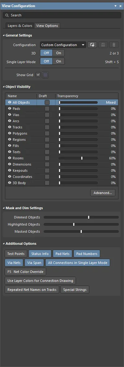
Display-related settings are configured in the View Configuration panel.
Besides the standard ways of accessing a panel (from the Panels button at the bottom right of the design space or the View » Panels menu), the View Configuration panel can also be accessed by using the L or Ctrl+D shortcut keys (to open the panel with the Layers & Colors or View Options tab displayed, respectively) or by clicking the color swatch on the Layer Sets control at the bottom left of the design space ( ).
).
The panel content is divided into two tabs. Click on a tab at the top of the panel to display the options available on that tab:
-
Layers and Colors tab – includes options to control the visibility of available layers, add, rename or delete mechanical layers, and configure the color and visibility of special system display features, such as pad holes, the origin marker and DRC errors.
-
View Options tab – includes options to select, save or load the Configuration of layer colors/visibility, configure the visibility of object-types, control the masking and dimming levels, and configure other display-related options.
The options that are available will depend on the current Layout Mode (2D or 3D).
In 3D Layout mode, the
Section View tab is also available in the
View Configuration panel. Use this tab to configure the section view of your PCB –
learn more.
Configuring Layer Visibility
Each layer can be displayed or hidden from the Layers region of the Layers & Colors tab of the View Configuration panel. Click the visibility icon ( ) to toggle the visibility off and on.

Manage layer visibility using the visibility icons
Where appropriate, each group also includes a visibility icon. For example, in the image above:
-
The visibility icon to the left of the string Component Layer Pairs (C) toggles the visibility of all component layers on/off.
-
The visibility icon to the left of the string Top toggles the visibility of all top side component layers. The Bottom side layers can also be displayed/hidden in the same way.
Controlling Layer Visibility from the Keyboard
In a busy PCB design, layers are often toggled on and off during the design process. To help with this, layer visibility can be changed using keystrokes in the following way:
-
Press the L shortcut key to display/make the Layers & Colors tab of the View Configuration panel active. The panel's title bar will become colored, indicating that it is the active element in the software.
-
Note that there are characters and numbers in curved brackets to the right of some of the layers and sets of layers, for example, Component Layer Pairs (C), and [1] Top (T). The character/number in curved brackets is a keyboard shortcut key. As an example, press the L shortcut to make the panel active, then press the T shortcut to toggle the visibility of the Top signal layer.
-
If you have accessed a set of layers, press Spacebar to toggle the visibility of all layers in that set.
-
If you have accessed a layer, its visibility will toggle immediately and the Spacebar can then be used to toggle it again.
-
Press the Up or Down arrow keys to move up or down through the list, for example, to access a specific mechanical layer or a pair of component layers. You can then use the Spacebar to toggle the visibility of that layer/layer pair.
-
The number within the square brackets indicates which physical copper layer that signal or plane layer is, in the layer stack. Consider the string, [6] Bottom (B), the [6] indicates that this is the 6th copper layer in the layer stack, Bottom is the user-defined name assigned to this layer in the Layer Stack Manager, and the (B) is the shortcut key to toggle the visibility of that layer.
-
Shortcut keys for signal and plane layers stop at (9), the last available numeric key on the keyboard.
Layer Sets
A Layer Set is a named set of visible layers. Use the Layers Sets drop-down in the Layers region of the Layers & Colors tab of the View Configuration panel to select an existing Layer Set; the display will update to only show the layers enabled for that Layer Set. Any number of user-defined Layer Sets can be created, and the currently selected Layer Set can also be edited.
-
To create a new user-defined Layer Set, define layer visibility in the Layers region as required and then click the
 button. The set will appear as My Layers in the drop-down. Each subsequent Layer Set added will be numbered.
-
To change configuration of enabled layers for an existing user-defined Layer Set, select it in the Layers Sets drop-down, configure layer visibility as required, and then click the
 button to save the changes in the Layer Set.
-
To rename an existing user-defined Layer Set, select it in the Layers Sets drop-down and enter the required name in the Layer Sets fields. Note that renaming a Layer Set does not require a save action, a new name will be saved automatically.
-
To delete an existing user-defined Layer Set, select it in the Layers Sets drop-down and click the
 button.
-
To import the desired Layer Set from a PCB Layer Set File
(*.layerset) or export the desired Layer Set as a PCB Layer Set File, use the Import and Export buttons, respectively.
Use the following techniques to switch visible Layer Sets:
-
Layer Set drop-down in the View Configuration panel
-
Design » Manage Layer Sets sub-menu
-
Layer Set control - accessed by clicking the LS part of the button to the left of the layer tabs at the bottom of the design space (
 ).
).
System Colors
The System Colors region can be used to configure the colors used on the PCB for the items listed. Colors and visibility are configured using the usual techniques.
Layer Tabs
The tabs associated with each layer currently set visible in the View Configuration panel are located along the bottom edge of the design space.

They allow you to switch the active layer (the layer you will be placing objects on) and give a visual indication of which layers are currently being displayed and which is the active layer (the highlighted tab). If there are more layer tabs than can be displayed at one time, use the arrows  to scroll through the tabs.
Layer colors will be displayed to the left of the layer tabs and double-clicking the layer color will launch the Choose Color dialog.
Double-click on the layer name to open the Edit Layer dialog from where you can edit the layer name (and net name for an internal plane layer).

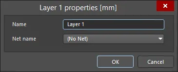
The Edit Layer dialog
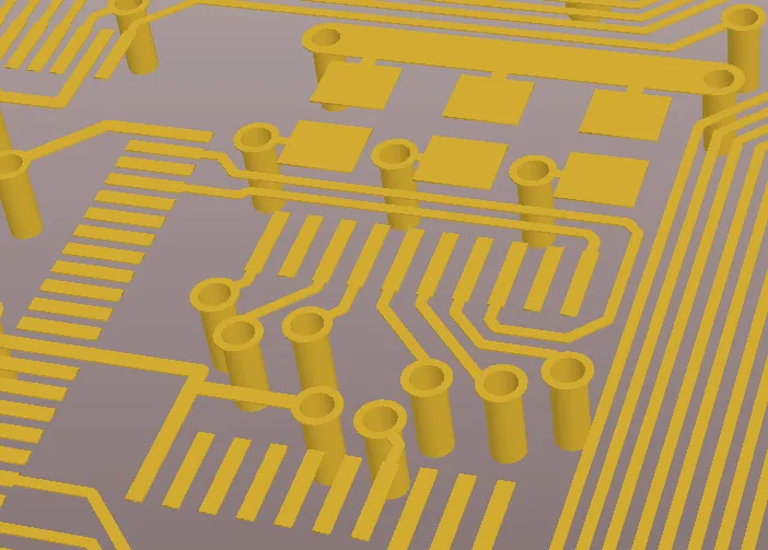
Single-Layer Mode
Single-Layer 2D Display Mode
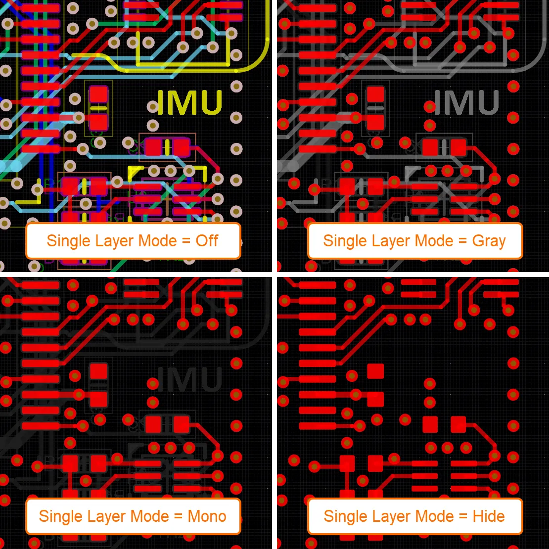
Integrated with Board Insight are the Single-Layer mode features, which are configured on the PCB Editor - Board Insight Display page of the Preferences dialog. Single Layer mode displays the contents of the current layer while hiding or dimming the contents of all other layers. As well as hiding all objects on all other layers to display only the contents of the current layer, Single-Layer mode has grayscale and monochrome display modes. Converting all other layer colors to grayscale or monochrome lets you retain the spatial relationship information about the location of other objects in the design, without distracting you from the layer of interest. To cycle between the full display and each of the enabled single-layer modes, press the Shift+S shortcut. With each press of Shift+S, the software moves to the next enabled mode, ultimately returning to the full display mode. Single-layer modes are enabled on the PCB Editor - Board Insight Display page of the Preferences dialog. Disable (uncheck) any modes you do not want to be included when you press Shift+S. These settings apply to all designs in this installation of Altium Designer.
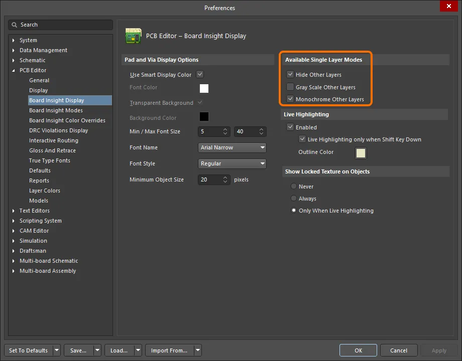
The single-layer modes available are:
-
Hide Other Layers - all other layers are hidden; only the contents of the active (current) layer are shown.
-
Gray Scale Other Layers - all other layers are displayed in a shade of gray derived from their current layer color; the active layer is shown in its standard color.
-
Monochrome Other Layers - all other layers are displayed in the same shade of gray; the active layer is shown in its standard color.
The below images show the regular multi-layer display and the three single-layer display modes.
The currently chosen single-layer mode is displayed in the General Settings region on the View Options tab of the View Configuration panel. Click the mode link (next to the On button) to access the PCB Editor - Board Insight Display page of the Preferences dialog from where you can configure the available single-layer modes as required.
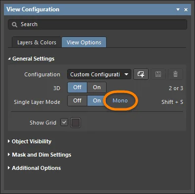
Use the Masked Objects slider in the Mask and Dim Settings region of the View Options tab of the View Configuration panel to control the brightness of other layers in the Gray or the Mono Single Layer modes.
Single-Layer 3D Display Mode
Single-layer mode is also available when the board is displayed in 3D Layout Mode. Use this for tasks such as examining the quality of routing on a specific layer or the quality of a power plane layer. While in single-layer mode, use the Ctrl+Shift+Wheel Roll shortcut to step through the layers.
Permanently Display a Layer in the Single Layer Mode Display
To include a layer in the Single Layer Mode display, perform a Ctrl+Click on the eye icon associated with the desired layer on the Layers & Colors tab of the View Configuration panel to add that layer into Single Layer Mode display; a square will appear behind the eye icon ( ) to denote that layer will be permanently displayed in Single Layer Mode.
Viewing the Board from the Bottom Side
To view the board from the bottom side (essentially, to flip the board), enable the View From Bottom Side option in the Layers region of the Layers & Colors tab of the View Configuration panel, select the View » Flip Board command from the main menus or use the Ctrl+F keyboard shortcut.
All actions and editing commands are supported for flipped boards/components. The coordinate space remains logically the same, i.e. the design space origin moves from the bottom-left to the bottom-right. The current grid position increases in the X (horizontal) direction as you move the mouse from right to left instead of the normal left to right. Any output generated while the view is flipped will maintain the correct 'viewed-from-top' coordinate information.
When the board/component is flipped, the layer drawing order is also changed using a logical pair-swapping process, which means that Top Overlay will swap positions in the current layer drawing order with Bottom Overlay, Top Layer with Bottom Layer, Mid-Layer 1 with Mid-Layer 30, Internal Plane 1 with Internal Plane 16, and so on. The drawing order of mechanical layers is not changed.
Controlling Object Visibility
As well as controlling the display of objects in the design space by toggling layers on and off, another approach is to control the visibility and transparency of objects based on their object type. When in 2D Layout mode, use the options provided by the Object Visibility region of the View Options tab of the View Configuration panel to configure object visibility and transparency by their type.

The Object Visibility section of the panel's View Options tab
-
– control the visibility of specific object types by clicking the appropriate visibility icon. Click the All Objects visibility icon to toggle the visibility of all objects then enable the visibility of specific object types.
-
Name – lists all objects that may be adjusted visually.
-
Draft – enable to display the object type as an outline.
-
Transparency – adjust the transparency of that object type using the slider bar or click the value and enter the desired percentage manually between 0 and 100 (0% is fully visible (solid); 100% is fully transparent (invisible)). Setting an object to transparent means you can see when one object covers another object, for example, where the end of a track segment meets a pad.
-
Advanced – click to open the Object Visibility dialog, where you can set a common transparency level for a particular object across different layers and set different transparencies for different objects on a specific layer.
Easily restore your preferred visibility settings by creating a Custom Configuration in the General Settings region of this panel.
Mask and Dim Settings
To help manage the display of the large number of objects that can exist even in a simple PCB design, the PCB editor has the ability to fade objects that are not of interest. For example, if you click on a net in the Nets mode of the PCB panel and the panel drop-down is set to Dim or Mask, then all objects that do not belong to that net are faded. This allows you to more easily focus your attention on a specific design element, such as a net or a class of nets, class of components, objects targeted by a certain design rule, and so on. Use sliders in the Mask and Dim Settings region of the View Options tab of the View Configuration panel to configure levels of masking and dimming.

The Mask and Dim Settings region of the View Configuration panel's View Options tab
Managing Configurations
A configuration is a pre-packed definition of layer color and layer visibility settings. Select an existing configuration from the Configuration drop-down in the General Settings region of the View Options tab of the View Configuration panel, or use the buttons next to the drop-down to create, save, or delete a configuration. Custom configurations save both of the current/last used 2D and 3D display settings.
-
– click to create a new Custom Configuration then type in a new name and click the button.
-
– click to save when you create a new Custom Configuration or if have edited the currently selected Custom Configuration.
-
– click to delete the currently selected Custom Configuration.
-
Custom configurations that have been created and saved are automatically loaded and available for selection from the Configuration field's drop-down listing.
-
Use the Load View Configuration option from the Configuration field's drop-down to load a configuration file stored in a location that is non-standard for the current Altium Designer installation. Note that user-defined configurations are saved as a Complex Configuration (with the file extension
.config_complex), so you may need to change the File Type dropdown in the Open dialog when you are loading a custom configuration.
Additional Options
The Additional Options region of the View Options tab of the View Configuration panel offers additional options to control the view of specific elements.

The Additional Options section of the View Configuration panel's View Options tab
-
Test Points – enable this option to display additional information on pads and vias that have been configured as testpoints. A Pad or a Via can be configured as a testpoint by enabling the Fabrication and/or Assembly Testpoint options in the relevant mode of the Properties panel. Testpoints are indicated by adding the string
<Layer> Fab Testpoint or <Layer> Assy Testpoint to the pad/via.
-
Status Info – enable this option to have summary information, such as coordinate position and layer, displayed in the Status Bar when hovering over an object in the design space.
-
Pad Nets – enable this option to display the associated net name on a pad. Note that net names will only become visible if you are zoomed in close enough.
-
Pad Numbers – enable this option to display pad numbers. Note that pad numbers will only become visible if you are zoomed in close enough.
-
Via Nets – enable this option to display the relevant net name on a via. Note that net names will only become visible if you are zoomed in close enough.
-
Via Span – enable this option to display the length in which the via is allowed to span. The properties of placed vias (diameter, hole size, etc.,) are then defined either by design rules or manually. Note that net names will only become visible if you are zoomed in close enough. The layer numbers in the via span can be displayed inside all via types.
-
All Connections in Single Layer Mode – enable this option to always display all of the connection lines when in Single Layer Mode. With this option disabled, all connection lines that do not start or end on the current layer are also hidden when switching to Single Layer Mode as it is assumed that they are not relevant.
-
Net Color Override – each net can be assigned a color. To configure the color, double-click on that net's name in the Nets mode of the PCB panel; the Edit Net dialog will open. The color is automatically applied to that net's connection lines and also can be applied to the routing by enabling this option. Color is applied to the routing in accordance with the current settings in the PCB Editor – Board Insight Color Overrides page of the Preferences dialog, where you choose a Pattern option to define how the color is applied and choose a Zoom Behavior to define when the color is applied. Press the F5 shortcut to toggle the Net Color Override option on and off.
-
Use Layer Colors for Connection Drawing – enable this option to display the connection lines using the colors of the start and end layers that the connection line travels between. The connection lines are displayed in pure layer color at the object they start/end at, morphing between those layer colors along the length of the connection line. This feature is helpful when you are routing a multi-layer board as it indicates the target layer that the connection being routed, must go to. Note that color morphing is only applied to connections that travel from one layer to another. If the connection starts and ends on the same layer, it retains the assigned net color.
-
Repeated Net Names on Tracks – enable to show repeated net names on tracks.
-
Special Strings – when the option is enabled, any placed Strings that are formed from converted Special Strings will be superimposed (labeled) with the unconverted Special String name. Zoom in on a String to see its label overlay.

