Исторически печатные платы (PCB) разводились в двумерном пространстве проектирования, где различные слои платы обозначались цветами. Однако физическая плата — это трёхмерный объект, поэтому проектировщику PCB приходится брать многослойное 2D‑представление на экране и «переводить» его в 3D‑представление у себя в голове.
Существенные улучшения 3D‑видеокарт и поддерживающих программных технологий позволили Altium разработать решение этой проблемы — полноценное трёхмерное редактирование PCB. Это больше, чем простая визуализация: 3D‑возможности Altium Designer позволяют:
-
Выполнять 3D‑проверку зазоров (clearance) — компоненты можно точно выравнивать относительно друг друга и корпуса, как требуется.
-
Визуально находить разъёмы и другие компоненты, к которым нужен доступ для обслуживания.
-
Лучше определять производственные процессы и порядок сборки, зная, что все механические ограничения учтены.
-
Создавать более подробные инструкции по ручной сборке, руководства пользователя и инструкции, используя изображения, гораздо ближе к тому, что реально увидит человек.
-
Экспериментировать с различными цветами паяльной маски, чтобы получить более эстетичный продукт, хорошо сочетающийся с корпусом и окружением.
-
Проще привлекать ключевых заинтересованных лиц, показывая им более наглядный и «осязаемый» вид конечного изделия.

2D- и 3D‑виды одной и той же области платы.
Режимы отображения
Altium Designer поддерживает отображение и редактирование платы в 2D или в 3D; эти режимы называются display modes. Выберите нужный режим в меню View или нажмите сочетание 1, 2 или 3, чтобы сразу переключиться в соответствующий режим.
Существует три режима отображения, каждый со своими функциями.
-
Board Planning Mode (горячая клавиша 1) — используйте для задания контура платы, а также для размещения и настройки линий разделения (split lines) и линий сгиба (bending lines) в rigid‑flex‑проекте. Линии разделения используются для разбиения платы на области, и каждой области затем можно назначить свой стек слоёв. Подробнее об областях платы, линиях разделения и линиях сгиба см. в Defining the Layer Stack.
-
2D Layout Mode (горячая клавиша 2) — традиционный 2D‑вид PCB с несколькими слоями. В Altium Designer есть набор функций для управления отображением платы, называемый Board Insight System.
-
3D Layout Mode (горячая клавиша 3) — полноценное 3D‑проектирование. Совместите 3D‑режим отображения с 3D‑мышью, чтобы просматривать и управлять загруженной 3D‑платой так, будто вы держите её в руке. Подробнее об управлении видом PCB в 3D см. на странице Controlling the 3D View.
Для 3D Layout Mode требуется видеокарта с поддержкой DirectX 9 или новее, с Shader Model 3 или новее.
 Одна и та же плата показана в режимах Board Planning, 2D Layout и 3D Layout.
Панель View Configuration
То, что в данный момент отображается в рабочей области редактора PCB, и то, как это отображается, можно настроить на панели View Configuration. Сюда входят видимость и цвет слоёв, видимость и прозрачность объектов, уровни маскирования и затемнения, текущий режим одиночного слоя, а также ряд дополнительных функций отображения рабочей области, например показ имён цепей (net names) на площадках, переходных отверстиях (via) и дорожках.
 Настройки, связанные с отображением, задаются на панели
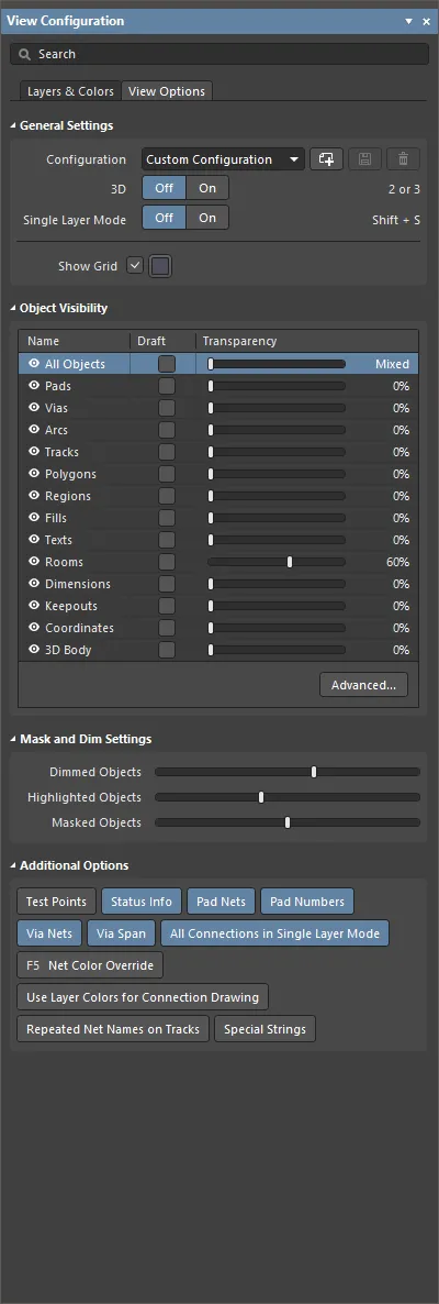
в View Configuration.
Помимо стандартных способов открытия панели (кнопкой Panels в правом нижнем углу рабочей области или через меню View » Panels ), панель View Configuration также можно открыть с помощью горячих клавиш L или Ctrl+D (чтобы открыть панель с активной вкладкой Layers & Colors или View Options соответственно) либо щёлкнув по образцу цвета (color swatch) в элементе управления Layer Sets в левом нижнем углу рабочей области ( ).
).
Содержимое панели разделено на две вкладки. Щёлкните вкладку в верхней части панели, чтобы отобразить доступные на ней параметры:
-
Layers and Colors вкладка — включает параметры управления видимостью доступных слоёв, добавления, переименования или удаления mechanical layers, а также настройки цвета и видимости специальных системных элементов отображения, таких как отверстия площадок, маркер начала координат и ошибки DRC.
-
View Options вкладка — включает параметры выбора, сохранения или загрузки конфигурации цветов/видимости слоёв, настройки видимости типов объектов, управления уровнями маскирования и затемнения, а также другие параметры, связанные с отображением.
Доступные параметры зависят от текущего Layout Mode (2D или 3D).
В режиме 3D Layout на панели
View Configuration также доступна вкладка
Section View. Используйте её для настройки секущего вида (section view) вашей PCB —
узнать больше.
Настройка видимости слоёв
Каждый слой можно показать или скрыть в области Layers на вкладке Layers & Colors панели View Configuration. Нажмите значок видимости ( ), чтобы переключать видимость.

Управляйте видимостью слоёв с помощью значков видимости
Где это уместно, каждая группа также включает значок видимости. Например, на изображении выше:
-
Значок видимости слева от строки Component Layer Pairs (C) переключает видимость all слоёв компонентов (component layers) вкл./выкл.
-
Значок видимости слева от строки Top переключает видимость all top side слоёв компонентов. Слои стороны Bottom также можно показывать/скрывать таким же образом.
Controlling Layer Visibility from the Keyboard
В насыщенном проекте PCB слои часто включают и выключают в процессе разработки. Чтобы упростить это, видимость слоёв можно менять с клавиатуры следующим образом:
-
Нажмите горячую клавишу L, чтобы отобразить/сделать активной вкладку Layers & Colors панели View Configuration. Заголовок панели окрасится, показывая, что она является активным элементом в программе.
-
Обратите внимание: справа от некоторых слоёв и наборов слоёв в круглых скобках указаны символы и цифры, например Component Layer Pairs (C) и [1] Top (T). Символ/цифра в круглых скобках — это клавиатурное сокращение. Например, нажмите сочетание L, чтобы сделать панель активной, затем нажмите T, чтобы переключить видимость верхнего сигнального слоя (Top).
-
Если вы выбрали набор слоёв, нажмите Spacebar, чтобы переключить видимость всех слоёв в этом наборе.
-
Если вы выбрали слой, его видимость переключится сразу, и затем Spacebar можно использовать, чтобы переключить её снова.
-
Нажимайте клавиши со стрелками Up или Down, чтобы перемещаться вверх/вниз по списку, например чтобы выбрать конкретный mechanical layer или пару слоёв компонентов. Затем можно использовать Spacebar, чтобы переключить видимость этого слоя/пары слоёв.
-
Число в квадратных скобках показывает, каким по счёту физическим медным слоем является данный сигнальный слой или слой Plane в стеке слоёв. Рассмотрим строку [6] Bottom (B): [6] означает, что это 6‑й медный слой в стеке, Bottom — пользовательское имя, назначенное этому слою в Layer Stack Manager, а (B) — горячая клавиша для переключения видимости этого слоя.
-
Горячие клавиши для сигнальных слоёв и слоёв Plane заканчиваются на (9) — последней доступной цифровой клавише на клавиатуре.
Наборы слоёв
Набор слоев — это именованный набор видимых слоев. Используйте раскрывающийся список Layers Sets в области Layers на вкладке Layers & Colors панели View Configuration, чтобы выбрать существующий Набор слоев; отображение обновится и будет показывать только те слои, которые включены для этого Набора слоев. Можно создать любое количество пользовательских Наборов слоев, а также редактировать текущий выбранный Набор слоев.
-
Чтобы создать новый пользовательский Набор слоев, задайте видимость слоев в области Layers нужным образом, затем нажмите кнопку
 . Набор появится в раскрывающемся списке как My Layers. Каждый последующий добавленный Набор слоев будет пронумерован.
-
Чтобы изменить конфигурацию включенных слоев для существующего пользовательского Набора слоев, выберите его в раскрывающемся списке Layers Sets, настройте видимость слоев как требуется, затем нажмите кнопку
 , чтобы сохранить изменения в Наборе слоев.
-
Чтобы переименовать существующий пользовательский Набор слоев, выберите его в раскрывающемся списке Layers Sets и введите нужное имя в поля Layer Sets. Обратите внимание: переименование Набора слоев не требует сохранения — новое имя будет сохранено автоматически.
-
Чтобы удалить существующий пользовательский Набор слоев, выберите его в раскрывающемся списке Layers Sets и нажмите кнопку
 .
.
-
Чтобы импортировать нужный Набор слоев из файла PCB Layer Set File
(*.layerset) или экспортировать нужный Набор слоев как PCB Layer Set File, используйте кнопки Import и Export соответственно.
Используйте следующие способы для переключения видимых Наборов слоев:
-
Layer Set раскрывающийся список в панели View Configuration
-
Design » Manage Layer Sets подменю
-
Layer Set элемент управления — доступен при щелчке по части LS кнопки слева от вкладок слоев в нижней части рабочего пространства (
 ).
).
Системные цвета
Область System Colors можно использовать для настройки цветов, применяемых на плате для перечисленных элементов. Цвета и видимость настраиваются обычными способами.
Вкладки слоев
Вкладки, связанные с каждым слоем, который в данный момент установлен как видимый в панели View Configuration, расположены вдоль нижнего края рабочего пространства.

Они позволяют переключать активный слой (слой, на котором вы будете размещать объекты) и дают визуальную индикацию того, какие слои сейчас отображаются и какой слой является активным (подсвеченная вкладка). Если вкладок слоев больше, чем можно отобразить одновременно, используйте стрелки  для прокрутки вкладок.
Цвета слоев отображаются слева от вкладок слоев; двойной щелчок по цвету слоя откроет диалог Choose Color.
Дважды щелкните по имени слоя, чтобы открыть диалог Edit Layer, где можно отредактировать имя слоя (а также имя цепи для внутреннего слоя плоскости).

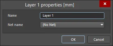
Диалог Edit Layer
Режим одного слоя
Режим 2D-отображения одного слоя
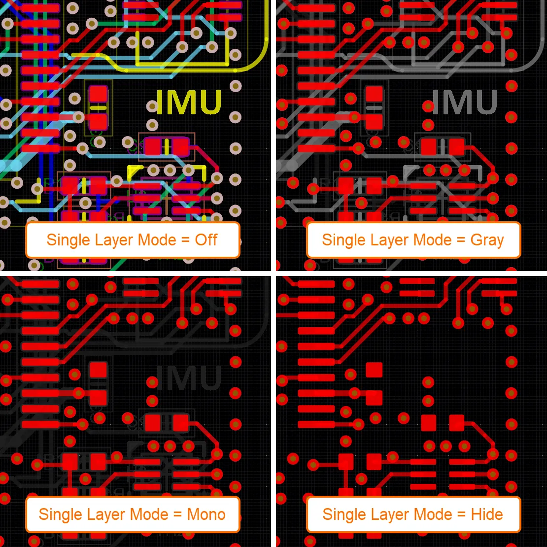
В Board Insight интегрированы функции режима Single-Layer, которые настраиваются на странице PCB Editor - Board Insight Display диалога Preferences. Режим одного слоя отображает содержимое текущего слоя, скрывая или приглушая содержимое всех остальных слоев. Помимо скрытия всех объектов на всех остальных слоях, чтобы показывать только содержимое текущего слоя, режим Single-Layer имеет режимы отображения в градациях серого и монохромный. Преобразование цветов всех остальных слоев в градации серого или монохром позволяет сохранять информацию о взаимном расположении других объектов в проекте, не отвлекаясь от интересующего слоя. Чтобы циклически переключаться между полным отображением и каждым из включенных режимов одного слоя, нажмите сочетание клавиш Shift+S. При каждом нажатии Shift+S программа переходит к следующему включенному режиму, в итоге возвращаясь к режиму полного отображения. Режимы одного слоя включаются на странице PCB Editor - Board Insight Display диалога Preferences. Отключите (снимите флажок) те режимы, которые не должны участвовать при нажатии Shift+S. Эти настройки применяются ко всем проектам в данной установке Altium Designer.
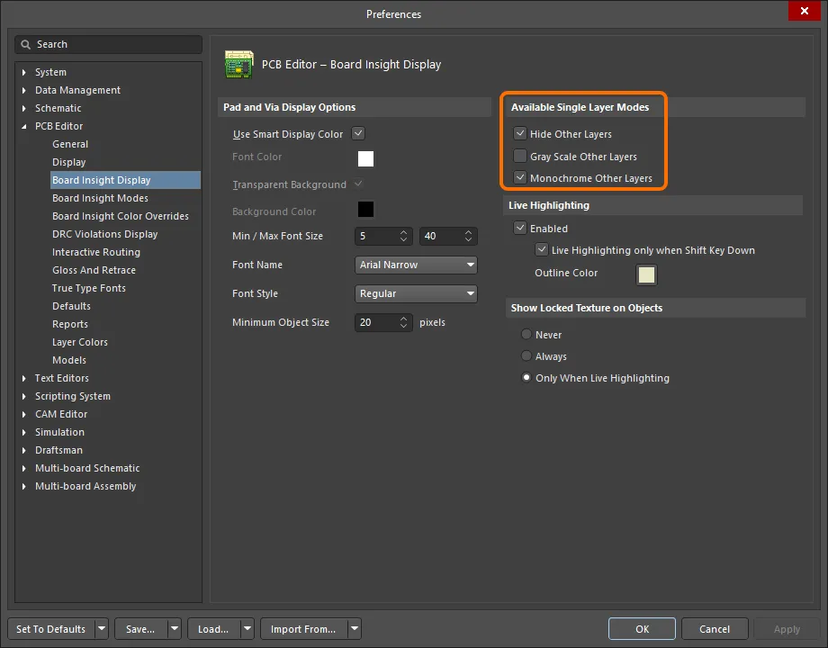
Доступны следующие режимы одного слоя:
-
Hide Other Layers - все остальные слои скрыты; показывается только содержимое активного (текущего) слоя.
-
Gray Scale Other Layers - все остальные слои отображаются в оттенке серого, полученном из их текущего цвета слоя; активный слой показан в своем стандартном цвете.
-
Monochrome Other Layers - все остальные слои отображаются в одном и том же оттенке серого; активный слой показан в своем стандартном цвете.
На изображениях ниже показаны обычное многослойное отображение и три режима отображения одного слоя.
Текущий выбранный режим одного слоя отображается в области General Settings на вкладке View Options панели View Configuration. Щелкните ссылку режима (рядом с кнопкой On ), чтобы перейти на страницу PCB Editor - Board Insight Display диалога Preferences, где можно настроить доступные режимы одного слоя.
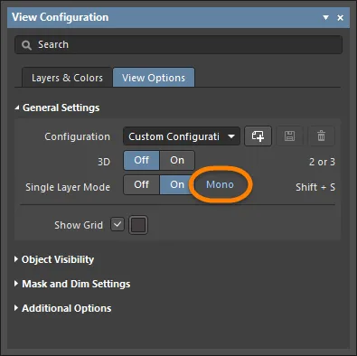
Используйте ползунок Masked Objects в области Mask and Dim Settings на вкладке View Options панели View Configuration, чтобы управлять яркостью других слоев в режимах Gray или Mono Single Layer.
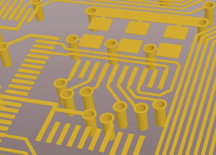
Режим 3D-отображения одного слоя
Режим одного слоя также доступен, когда плата отображается в 3D Layout Mode. Используйте его для задач, таких как оценка качества трассировки на конкретном слое или качества слоя плоскости питания. Находясь в режиме одного слоя, используйте сочетание клавиш Ctrl+Shift+Wheel Roll, чтобы пошагово переключаться между слоями.
Постоянное отображение слоя в режиме Single Layer
Чтобы включить слой в отображение режима Single Layer Mode, выполните Ctrl+Click по значку «глаз» нужного слоя на вкладке Layers & Colors панели View Configuration, чтобы добавить этот слой в отображение Single Layer Mode; за значком «глаз» появится квадрат ( ), обозначающий, что этот слой будет постоянно отображаться в режиме Single Layer Mode.
Просмотр платы со стороны низа
Чтобы просмотреть плату снизу (по сути, перевернуть плату), включите параметр View From Bottom Side в области Layers на вкладке Layers & Colors панели View Configuration, выберите команду View » Flip Board в главном меню или используйте сочетание клавиш Ctrl+F.
Для перевернутых плат/компонентов поддерживаются все действия и команды редактирования. Координатное пространство логически остается тем же, т.е. начало координат в рабочем пространстве смещается из нижнего левого угла в нижний правый. Текущая позиция по сетке увеличивается по X (горизонтали), когда вы перемещаете мышь справа налево, вместо обычного движения слева направо. Любые выходные данные, сформированные при перевернутом виде, сохранят корректную координатную информацию «вид сверху».
Когда плата/компонент перевернуты, порядок отрисовки слоев также изменяется с использованием логического процесса попарной перестановки, что означает, что Top Overlay поменяется местами в текущем порядке отрисовки слоев с Bottom Overlay, Top Layer — с Bottom Layer, Mid-Layer 1 — с Mid-Layer 30, Internal Plane 1 — с Internal Plane 16 и так далее. Порядок отрисовки механических слоев не изменяется.
Управление видимостью объектов
Помимо управления отображением объектов в рабочем пространстве путем включения и выключения слоев, можно также управлять видимостью и прозрачностью объектов в зависимости от их типа. В режиме 2D Layout используйте параметры, предоставляемые областью Object Visibility на вкладке View Options панели View Configuration, чтобы настроить видимость и прозрачность объектов по их типу.

Раздел Object Visibility на вкладке View Options панели
-
— управление видимостью конкретных типов объектов путем щелчка по соответствующему значку видимости. Щелкните значок видимости All Objects, чтобы переключить видимость всех объектов, затем включите видимость нужных типов объектов.
-
Name — перечисляет все объекты, внешний вид которых можно настраивать.
-
Draft — включите, чтобы отображать тип объекта в виде контура.
-
Transparency — настройте прозрачность этого типа объекта с помощью ползунка или щелкните значение и вручную введите нужный процент от 0 до 100 (0% — полностью видимый (непрозрачный); 100% — полностью прозрачный (невидимый)). Установка объекта как прозрачного позволяет видеть, когда один объект перекрывает другой, например, в месте, где конец сегмента дорожки примыкает к площадке.
-
Advanced — щелкните, чтобы открыть диалог Object Visibility, где можно задать общий уровень прозрачности для конкретного объекта на разных слоях и установить разную прозрачность для разных объектов на конкретном слое.
Быстро восстановить предпочитаемые настройки видимости можно, создав Custom Configuration в области General Settings этой панели.
Настройки маски и затемнения
Чтобы упростить управление отображением большого количества объектов, которые могут присутствовать даже в простом проекте печатной платы, редактор PCB умеет «приглушать» (fade) объекты, которые в данный момент не представляют интереса. Например, если щелкнуть по цепи (net) в режиме Nets панели PCB и в выпадающем списке панели выбрано Dim или Mask, то все объекты, не относящиеся к этой цепи, будут приглушены. Это позволяет легче сосредоточиться на конкретном элементе проекта, например на цепи или классе цепей, классе компонентов, объектах, на которые нацелено определенное правило проектирования, и т. п. Используйте ползунки в области Mask and Dim Settings на вкладке View Options панели View Configuration, чтобы настроить уровни маскирования и приглушения.

Область Mask and Dim Settings на вкладке View Options панели View Configuration
-
Dimmed Objects – объекты, которые сейчас приглушены, сохраняют свой цвет, но становятся бледнее. Этот ползунок задает, насколько сильно приглушенные объекты «выцветают». Приглушенные объекты можно редактировать.
Чтобы увеличить или уменьшить уровень приглушения, также можно использовать команды
View » Increase Mask Level (сочетание клавиш:
]) или
View » Decrease Mask Level (сочетание клавиш:
[) из главного меню, соответственно.
-
Highlighted Objects – когда включен режим Dim и вы щелкаете по объекту в панели, например по цепи в режиме Nets панели PCB, эта цепь дополнительно подсвечивается, а все остальные цепи приглушаются. Подсвеченные объекты «выбеливаются», чтобы выделяться. Этот ползунок управляет количеством белого, добавляемого к подсвеченным объектам.
-
Masked Objects – объекты, которые сейчас замаскированы, отображаются серым и не могут редактироваться. Этот ползунок задает, насколько сильно замаскированные объекты «выцветают».
Управление конфигурациями
Конфигурация — это заранее подготовленный набор настроек цвета слоев и их видимости. Выберите существующую конфигурацию в выпадающем списке Configuration в области General Settings вкладки View Options панели View Configuration или используйте кнопки рядом с выпадающим списком, чтобы создать, сохранить или удалить конфигурацию. Пользовательские конфигурации сохраняют как текущие/последние использованные настройки отображения 2D и 3D.
-
– нажмите, чтобы создать новую пользовательскую конфигурацию, затем введите новое имя и нажмите кнопку .
-
– нажмите, чтобы сохранить при создании новой пользовательской конфигурации или если вы отредактировали текущую выбранную пользовательскую конфигурацию.
-
– нажмите, чтобы удалить текущую выбранную пользовательскую конфигурацию.
-
Созданные и сохраненные пользовательские конфигурации загружаются автоматически и доступны для выбора в выпадающем списке поля Configuration.
-
Используйте параметр Load View Configuration в выпадающем списке поля Configuration, чтобы загрузить файл конфигурации, сохраненный в нестандартном для текущей установки Altium Designer месте. Обратите внимание: пользовательские конфигурации сохраняются как Complex Configuration (с расширением файла
.config_complex), поэтому при загрузке пользовательской конфигурации может потребоваться изменить выпадающий список File Type в диалоге Open.
Дополнительные параметры
Область Additional Options на вкладке View Options панели View Configuration предлагает дополнительные параметры для управления отображением отдельных элементов.

Раздел Additional Options на вкладке View Options панели View Configuration
-
Test Points – включите этот параметр, чтобы отображать дополнительную информацию на площадках (pads) и переходных отверстиях (vias), настроенных как тестовые точки (testpoints). Площадку или переходное отверстие можно настроить как тестовую точку, включив параметры Testpoint Fabrication и/или Assembly в соответствующем режиме панели Properties. Тестовые точки обозначаются добавлением строки
<Layer> Fab Testpoint или <Layer> Assy Testpoint к площадке/переходному отверстию.
-
Status Info – включите этот параметр, чтобы при наведении курсора на объект в рабочей области в Status Bar отображалась сводная информация, например координаты и слой.
-
Pad Nets – включите этот параметр, чтобы отображать имя связанной цепи (net) на площадке. Обратите внимание: имена цепей будут видны только при достаточном увеличении.
-
Pad Numbers – включите этот параметр, чтобы отображать номера площадок. Обратите внимание: номера площадок будут видны только при достаточном увеличении.
-
Via Nets – включите этот параметр, чтобы отображать соответствующее имя цепи на переходном отверстии. Обратите внимание: имена цепей будут видны только при достаточном увеличении.
-
Via Span – включите этот параметр, чтобы отображать длину (диапазон слоев), на которую разрешено «простираться» переходному отверстию. Свойства размещенных переходных отверстий (диаметр, размер отверстия и т. п.) затем задаются либо правилами проектирования, либо вручную. Обратите внимание: имена цепей будут видны только при достаточном увеличении. Номера слоев в диапазоне via span могут отображаться внутри всех типов переходных отверстий.
-
All Connections in Single Layer Mode – включите этот параметр, чтобы в режиме Single Layer Mode всегда отображались все линии соединений. Если параметр отключен, то при переключении в Single Layer Mode также скрываются все линии соединений, которые не начинаются и не заканчиваются на текущем слое, поскольку предполагается, что они не относятся к делу.
-
Net Color Override – каждой цепи можно назначить цвет. Чтобы настроить цвет, дважды щелкните по имени цепи в режиме Nets панели PCB; откроется диалог Edit Net dialog . Цвет автоматически применяется к линиям соединений этой цепи, а также может применяться к трассировке при включении этого параметра. Цвет применяется к трассировке в соответствии с текущими настройками на странице PCB Editor – Board Insight Color Overrides page диалога Preferences, где выбирается параметр Pattern, определяющий способ применения цвета, и Zoom Behavior, определяющий, когда цвет применяется. Нажмите сочетание клавиш F5, чтобы включать и выключать параметр Net Color Override.
-
Use Layer Colors for Connection Drawing – включите этот параметр, чтобы отображать линии соединений с использованием цветов начального и конечного слоев, между которыми проходит линия соединения. Линии соединений отображаются чистым цветом слоя у объекта, от которого они начинаются/на котором заканчиваются, и плавно переходят между цветами слоев по всей длине линии. Эта функция полезна при трассировке многослойной платы, так как показывает целевой слой, на который должна перейти прокладываемая связь. Обратите внимание: плавный переход цвета применяется только к соединениям, проходящим с одного слоя на другой. Если соединение начинается и заканчивается на одном и том же слое, оно сохраняет назначенный цвет цепи.
-
Repeated Net Names on Tracks – включите, чтобы показывать повторяющиеся имена цепей на дорожках.
-
Special Strings – когда параметр включен, любые размещенные Strings, сформированные из преобразованных Special Strings, будут накладываться (маркироваться) именем исходной, непреобразованной Special String. Увеличьте масштаб на String, чтобы увидеть наложенную подпись.


 Локализовано с помощью ИИ