
Fill

A placed Fill
A fill is a rectangular object that can be placed on any layer. When placed on a signal layer, a fill becomes an area of solid copper that can be used to provide shielding or to carry large currents. Fills of varying sizes can be combined to cover irregularly shaped areas and can also be combined with track or arc segments and be connected to a net.
Fills also can be placed on non-electrical layers. For example, place a fill on the Keep-Out layer to designate a 'no-go' area for auto-routing. Place a fill on a Power Plane, Solder Mask or Paste Mask layer to create a void on that layer. In the PCB Library Editor, fills can be used to define component footprints.
Fill Object
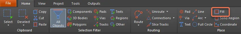
Fills are available for placement in the PCB editor by choosing choose Home | Place | Fill.
After launching the command, the cursor will change to a cross-hair and you will enter fill placement mode. Placement is made by performing the following sequence of actions:
- Click or press Enter to anchor the first corner of the fill.
- Move the cursor to adjust the size of the fill then click or press Enter to anchor the diagonally-opposite corner and complete placement of the fill.
- Continue placing further fills or right-click or press Esc to exit placement mode.
Additional actions that can be performed during placement are:
- Press the Tab key to pause the placement and access the Fill mode of the Inspector panel in which its properties can be changed on the fly. Click the design space pause button overlay (
 ) to resume placement.
 - Press the L key to flip the fill to the other side of the board. Note that this is only possible prior to anchoring the fill's first corner.
- Press the + and - keys (on the numeric keypad) to cycle forward and backward through all visible layers in the design to change the placement layer quickly.
- Press the Alt key to constrain the direction of movement to the horizontal or vertical axis depending on the initial direction of movement.
Graphical Editing
This method of editing allows you to select a placed fill object directly in the design space and change its size, shape or location graphically.
When a fill object is selected, the following editing handles are available:

A selected Fill
- Click and drag A to resize the fill in the vertical and horizontal directions simultaneously.
- Click and drag B to resize the fill in the vertical and horizontal directions separately.
- Click and drag C to rotate the fill about its center point.
- Click anywhere on the fill away from editing handles and drag to reposition it. While dragging, the fill can be rotated or mirrored:
- Press the Spacebar to rotate the fill counterclockwise or Shift+Spacebar for clockwise rotation. Rotation is in accordance with the value for the Rotation Step defined on the PCB Editor – General page of the System Preferences.
- Press the X or Y keys to mirror the fill along the X-axis or Y-axis.
Non-Graphical Editing
This method of editing uses the Inspector panel to modify the properties of a Fill object.

During placement, the Fill mode of the Inspector panel can be accessed by pressing the Tab key. Once the Fill is placed, all options appear.
After placement, the Fill mode of the Inspector panel can be accessed in one of the following ways:
- If the Inspector panel is already open, select the Fill object.
- With the fill selected, choose View | Schematic | Inspector from the main ribbons.
Editing Multiple Objects
The Inspector panel supports multiple object editing, where the property settings that are identical in all currently selected objects may be modified. When multiples of the same object type are selected manually, an Inspector panel field entry that is not shown as an asterisk (*) may be edited for all selected objects.
Fill Properties
All Fill object properties are available for editing in the Inspector panel when a placed Fill is selected in the design space.
Location
- (X/Y)
- X (first field) - the current X (horizontal) coordinate of the reference point of the fill, relative to the current design space origin. Edit to change the X position of the fill. The value can be entered in either metric or imperial; include the units when entering a value whose units are not the current default.
- Y (second field) - The current Y (vertical) coordinate of the reference point of the fill, relative to the current origin. Edit to change the Y position of the fill. The value can be entered in either metric or imperial; include the units when entering a value whose units are not the current default.
- Rotation - the fill's angle of rotation (in degrees), measured counterclockwise from zero (the 3 o'clock horizontal). Edit to change the rotation of the fill. Minimum angular resolution is 0.001°.
Properties
- Net - use the drop-down to select the net to which this fill belongs. All nets for the active board design will be listed in the drop-down list. Select No Net to specify that the fill is not connected to any net. The Net property of a primitive is used by the Design Rule Checker to determine if a PCB object is legally placed. If there is no net, click
 to go to a specific net within the design space.
- Layer - the layer on which the fill is placed. Fills can be placed on any layer other than the system layers. Use the drop-down to select a different layer.
- Area - specifies the area value of the fill object.
- Length - displays the length.
- Width - displays the width.
Paste Mask Expansion
- Rule - select to have the paste mask expansion for the fill follow the defined value in the applicable Paste Mask Expansion design rule. The associated value will be disabled if this option is chosen.
- Manual - select to override the applicable design rule and specify the paste mask expansion value for the fill in the field below.
Solder Mask Expansion
- Rule - select the checkbox to have the solder mask expansion for the fill follow the defined value in the applicable Solder Mask Expansion design rule. The associated value will be disabled if this option is chosen.
- Manual - select the checkbox to override the applicable design rule and specify the solder mask expansion value for the fill in the field below.