
Line
 A placed Track
In a PCB, a line and track are interchangeable terms. Placing a line, therefore, places a track. The Track mode of the Inspector panel is used when a line is placed. Tracks placed on a non-electrical layer are called lines, where they are used as general-purpose drawing elements to create component outlines, instructional information, keepout boundaries, and so on.
A Track segment is a primitive design object; a straight line of a defined width. You can use tracks to define a straight line in the PCB design space. Tracks are placed on a signal layer to form the electrical interconnections, or routing, between component pads. Tracks are also used in group design objects, such as dimensions and coordinates.
Line Object
Lines are available for placement in the PCB editor by choosing Home | Place | Line from the main menus.

After launching the command, the cursor will change to a crosshair and you will enter track placement mode. Placement is made by performing the following sequence of actions:
- Click or press Enter to anchor the starting point for the first track segment. If a routing-type placement command is being run and you click to start placement on an existing object, the track will adopt the net name of that object.
- Move the cursor to define the track segment then click or press Enter to anchor the end point for this first segment, which is also the starting point for the next connected segment.
- Continue to position the cursor then click or press Enter to anchor a series of vertex points that define the series of connected track segments.
- Right-click or press Esc to end the current series of connected track segments.
Additional actions that can be performed during placement include pressing the Tab key to pause the placement and access the Track mode of the Inspector panel from where its properties can be changed on the fly. Click the design space pause button overlay ( ) to resume placement.
Placement Modes
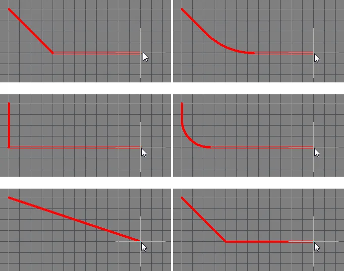
While placing track segments there are five available corner modes, four of which also have corner direction sub-modes. During placement:
- Press Shift+Spacebar to cycle through the five available corner modes.
- Press Spacebar to toggle between the two corner direction sub-modes.
- When in either of the arc corner modes, hold the "," or "." key to shrink or grow the arc. Hold the Shift key as you press to accelerate arc resizing.
- Press the 1 shortcut key to toggle between placing one segment per click (shown in the first five images below), or two segments per click (shown in the last image below). In the first mode, the hollow track segment is referred to as the look-ahead segment.
- Press the Backspace key to remove the last vertex.
Interactive Routing and the Applicable Design Rules
During Interactive Routing, the default behavior is for the software to ensure the track segments are placed in accordance with the applicable Electrical and Routing design rules. That means the software will not allow a new track segment to be placed that violates an existing track segment that belongs to a different net; instead, it will clip the track segment to meet the design rules. This interactive routing behavior is known as the Routing Conflict Resolution mode. The default mode is Stop at First Obstacle (the current mode is displayed on the Status bar). Press Shift+R to cycle through the available modes.
The term applicable design rules means all the rules that apply to the object being placed. The design rules engine works on a system where you scope exactly to which objects you want each rule to apply. During placement, the design rules engine is queried to determine the highest priority rule that applies in the current placement situation.
How the Routing Width is Determined
Unless the rules engine is disabled, the overriding behavior of the software is to always ensure that the routing width is within the range allowed by the applicable Routing Width design rule. A common approach is to allow a range of widths to be used for a net to give you flexibility in fitting in the route while satisfying the current carrying requirements of that net. Supporting this, the Routing Width design rule has Min, Preferred, and Max settings in the PCB Rules and Constraints Editor that can be configured to allow a range of widths or can be set the same to require a specific width. The width can also be configured as an Impedance and can also have a different range specified for each signal layer.
Options that can help select the most appropriate routing width when you begin routing are configured on the PCB Editor — Interactive Routing page of the System Preferences.
You can also use the Shift+W shortcut while routing to access a dialog where a different width can be selected, or you can press Tab to open the Inspector panel and type in a new Width value. The value chosen or entered must lie between the Min and Max settings defined in the applicable rule. If not, it is automatically clipped back to the nearest of these.
Interactive Routing Shortcuts
While you are routing, there are a number of shortcuts that are available. For example, you can press Shift+R to cycle through the available conflict resolution modes, or press Backspace to delete the last placed vertex (corner). To display a list of shortcuts while you are routing, press Shift+F1. A menu of available interactive shortcuts is displayed; select the required shortcut or press Esc to close the menu and use the shortcut key sequence.
Graphical Editing
This method of editing allows you to select a placed line object directly in the design space and change its size, shape, or location graphically.
When a line object is selected, the following editing handles are available:

A selected Track
- Click and drag A to reposition the end points of the track.
- Click and drag B to change the shape of the track.
The PCB editor includes sophisticated algorithms for moving track segments on the board so that the arrangement of the routing can be maintained. This sliding of track segments can be invoked interactively either by clicking to first select the track segment and then clicking and holding when the special cursor appears to slide the segment or by clicking and holding on a track segment and sliding it.
Non-Graphical Editing
This method of editing uses the Inspector panel mode to modify the properties of a line object.

During placement, the Track mode of the Inspector panel can be accessed by pressing the Tab key. Once the line is placed, all options appear.
After placement, the Track mode of the Inspector panel can be accessed in one of the following ways:
- If the Inspector panel is already open, select the track object.
- Right-click on a selected track and select Properties from the menu.
- From the PCB editor, choose View | PCB | Inspector from the main ribbons when a track is selected.
- From the PCB library editor, choose View | PCB Library | Inspector from the main ribbons when a track is selected.
Line Properties
When dragging a line in the design space, the Track properties are available for editing in the Inspector panel.

- Line Width - use this area to determine the desired width of the line.
- Current Layer - use the drop-down to determine which layer you prefer the line placed on.
All Track object properties are available for editing in the Inspector panel when a placed line is selected in the design space.
Location
- (X/Y)
- X (first field) - the current X (horizontal) coordinate of the reference point of the track relative to the current design space origin. Edit to change the X position of the track. The value can be entered in either metric or imperial; include the units when entering a value whose units are not the current default.
- Y (second field) - The current Y (vertical) coordinate of the reference point of the track relative to the current origin. Edit to change the Y position of the track. The value can be entered in either metric or imperial; include the units when entering a value whose units are not the current default.
Properties
- Net - use the drop-down to select the net to which this track belongs. All nets for the active board design will be listed in the drop-down list. If there is no net, click
 to jump to a specific net within the design space by specifying the net's name or clicking on a net manually using the cross-hair that appears. Select the Net link to open the Net mode of the Inspector panel then configure the properties.

Clicking the Nodes link in the Net mode opens the Edit Net dialog in which you can edit nets, add or remove physical pins for the specified net, and specify the track length for the net.

The key options of the Edit Net dialog are described below.
- Pins in Other Nets - lists all pins on the PCB. Pins that are currently assigned to a net include their net name in brackets. Select the pins you want to add to the net being edited. Use the control buttons to move selected pins into the current list or right-click to remove selected pins from the list using the context menu. After moving a pin from this list to the Pins in This Net list, you can right-click on the pin then select Remove One to move it back to the Pins in Other Nets list.
-
Pins in This Net - lists all pins in this net. Select the pins you want to remove from this net. Use the control buttons to move selected pins out of the current list or right-click and use the context menu to remove selected pins.
- Current Interactive Routing Settings - this region lists any current settings for interactive routing.
- Layer - use the drop-down to select the layer on which the track is located.
- Start (X/Y) - displays the current X/Y coordinate of the track start point relative to the current origin.
- Width - displays the current width of the track. Edit this field to change the track width within the range 0.001mil to 10000mil.
-
Length - displays the current length of the track. Edit this field to change the track length within the range 0.001mil to 10000mil.
- End (X/Y) - displays the current X/Y coordinate of the track end point relative to the current origin.
Paste Mask Expansion
- Rule/Manual - select the desired paste mask expansion configuration. Select Rule to have the paste mask expansion for the track follow the defined value in the applicable Paste Mask Expansion design rule. Select Manual to override the applicable design rule and specify the paste mask expansion value for the track. You can then enable and enter the desired measurement.
Solder Mask Expansion
- Rule/Manual - select the desired solder mask expansion configuration. Select Rule to have the solder mask expansion for the track follow the defined value in the applicable Solder Mask Expansion design rule. Select Manual to override the applicable design rule and specify the solder mask expansion value for the track. You can then enable and enter the desired measurement.