
Via
 A via that spans and connects from the top layer (red) to the bottom layer (blue),
and also connects to one internal power plane (green).
A via is a primitive design object. It is used to form a vertical electrical connection between two or more electrical layers of a PCB. Vias are a three-dimensional object, having a barrel-shaped body in the Z-plane, with a flat ring on each (horizontal) copper layer. The body of the via is formed when the board is drilled and through-plated during fabrication. In the X and Y planes, vias are circular, like round pads. The key difference between a via and a pad is that as well as being able to span all layers of the board (top to bottom), a via can also span from a surface layer to an internal layer, or between two internal layers.
Via Object
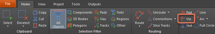
Vias are available for placement in the PCB editor by choosing Home | Place | Via from the main menus.Choose
After launching the command, the cursor will change to a crosshair and you will enter via placement mode:
- Position the cursor and click or press Enter to place a via.
- Continue placing further vias, or right-click or press Esc to exit placement mode.
Auto-placement of Vias During Routing
When a net is being interactively routed, you can cycle through the available signal layers by pressing the * key on the numeric keypad. Alternatively, use the Ctrl+Shift+Roll Mouse Wheel combination to move through the signal layers. When this is done, the software will automatically place a via in accordance with the applicable Routing Via Style design rule. Note that multiple Via Style design rules can be defined allowing different via sizes to be assigned to different nets.
Default Settings versus Design Rules
When a via is placed in free space, it is not possible for the software to apply a routing style design rule during placement. In this situation, the default via will be placed.
Graphical Editing
Vias cannot have their properties modified graphically other than their location. To move a via and also move the connected tracks, click and hold then move the via. The connected routing will remain attached to the via as it is moved.
If a via is being moved with the routing to create more routing or component space, it can be more efficient to re-route than move routing. The software includes a feature called Automatically Remove Loops, which can be enabled in the PCB Editor - Interactive Routing page of the Preferences dialog. With this feature enabled, you can route along a new path (starting and ending along the original routing). As soon as you right-click to exit the interactive routing mode, the old routing (loop) is removed, including any redundant vias.
Non-Graphical Editing
This method of editing uses the Inspector panel mode to modify the properties of a Via object.

During placement, the Via mode of the Inspector panel can be accessed by pressing the Tab key. Once the Via is placed, all options appear.
After placement, the Via mode of the Inspector panel can be accessed in one of the following ways:
- If the Inspector panel is already open, select the via object, right-click then choose Properties from the context menu.
- With the via selected, choose View | Schematic | Inspector from the main ribbons.
Via Properties
PCB Editor object properties are definable options that specify the visual style, content, and behavior of the placed object.
All Via properties are available for editing in the Inspector panel when a placed Via is selected in the design space.
Definition
- Net - use the drop-down to select the net to which this via belongs. All nets for the active board design will be listed in the drop-down list. If there is no net, click the edit button to jump to a specific net within the design space or click on a net manually using the cross-hair that appears. Select the Net link to open the Net mode of the Inspector panel:

- Net - lists the name of the net, which you may change if desired. Click the color box to select the desired color for the track. Click Define Custom Colors to expand the color palette to also display the Custom Color Palette. Use the horizontal slider in the center of the Custom Color Palette to select a base color then click anywhere on the palette to brighten or darken that color. Alternatively, enter the Hex or RGB values into the appropriate fields in the Custom Color Palette.
- Nodes - lists the number of nodes attached to the net. Click on the Nodes link to open the Edit Net dialog, which is described below.
- Net Class - lists the net's class.
- Net Length - lists the net's length.
- Loop Removal - enable to automatically remove any redundant loops that are part of this net.
- Name - when one or more via is/are selected, the via names are displayed by clicking the drop-down, which lists all of the via spans defined in the Layer Stack. All vias used on the board must be one of the via spans defined in the Layer Stack.
- (X/Y)
- X (first field) - this field shows the current X position of the center of the via relative to the current origin. Edit the value in the field to change the position of the via relative to the current origin. The value can be entered in either metric or imperial; include the units when entering a value whose units are not the current default. Default units (metric or imperial) are determined by the Units setting in the Other region of the Inspector panel in Board mode (accessed when no objects are selected in the design space) and are used if the unit is not specified.
- Y (second field) - this field shows the current Y position of the center of the via relative to the current origin. Edit the value in the field to change the position of the via relative to the current origin. The value can be entered in either metric or imperial; include the units when entering a value whose units are not the current default. Default units (metric or imperial) are determined by the Units setting in the Other region of the Inspector panel in Board mode (accessed when no objects are selected in the design space) and are used if the unit is not specified.
Via Stack
- Simple - select to choose a simple via.
- Diameter - enter the required diameter of the via. The via diameter is the same on all layers.
- Hole Size - this field displays the current hole size for the via. The value specifies the diameter of the hole (as a round, square or slotted shape) in mils or mm to be drilled in the via during fabrication. The hole size can be set from 0 to 1000mil and can be set larger than the via to define (copper-free) mechanical holes. Edit the value in this field to change the via hole size. The value can be entered in either metric or imperial; include the units when entering a value whose units are not the current default. Default units (metric or imperial) are determined by the Units setting in the Other region of the Inspector panel in Board mode (accessed when no objects are selected in the design space) and are used if the unit is not specified.
- Tolerance - setting hole tolerance attributes can help determine the fits and limits of your board. Specify the minimum (-) and maximum (+) tolerances for the hole. There is no default hole tolerance value.
- Top-Middle-Bottom - select to choose different diameters for the top layer, all internal signal layers, and the Bottom Layer.
- Displayed Layer(s) - click on a displayed layer to configure vias for that layer. The selected layer is highlighted.
- Diameter - click the drop-down then enter the required diameter of the via for the selected layer.
- Hole Size - this field displays the current hole size for the via. The value specifies the diameter of the hole (as a round, square, or slotted shape) in mils or mm to be drilled in the via during fabrication. The hole size can be set from 0 to 1000mil and can be set larger than the via to define (copper-free) mechanical holes. Edit the value in this field to change the via hole size. The value can be entered in either metric or imperial; include the units when entering a value whose units are not the current default. Default units (metric or imperial) are determined by the Units setting in the Other region of the Inspector panel in Board mode (accessed when no objects are selected in the design space), and are used if the unit is not specified.
- Tolerance - setting hole tolerance attributes can help determine the fits and limits of your board. Specify the minimum (-) and maximum (+) tolerances for the hole. There is no default hole tolerance value.
Solder Mask Expansion
- Rule - select to have the solder mask expansion for the via follow the defined value in the applicable Solder Mask Expansion design rule.
- Manual - select to override the applicable design rule and specify the solder mask expansion value for the via.
- Top - enter the top layer solder mask expansion value. The value can be entered in either metric or imperial; include the units when entering a value whose units are not the current default. Default units (metric or imperial) are determined by the Units setting in the Other region of the Inspector panel in Board mode (accessed when no objects are selected in the design space), and are used if the unit is not specified. This field is accessible only if Tented is not enabled.
- Tented - check if it is desired for any solder mask settings in the solder mask expansion design rules to be overridden, which results in no opening in the solder mask on the top layer of this via and is therefore tented. Disable this option and this via is affected by a solder mask expansion rule or specific expansion value.
- Bottom - enter the bottom layer solder mask expansion value. The value can be entered in either metric or imperial; include the units when entering a value whose units are not the current default. Default units (metric or imperial) are determined by the Units setting in the Other region of the Inspector panel in Board mode (accessed when no objects are selected in the design space) and are used if the unit is not specified.
- Tented - check if it is desired for any solder mask settings in the solder mask expansion design rules to be overridden, which results in no opening in the solder mask on the bottom layer of this via and is therefore tented. Disable this option and this via is affected by a solder mask expansion rule or specific expansion value.
- Top - enter the top layer solder mask expansion value. The value can be entered in either metric or imperial; include the units when entering a value whose units are not the current default. Default units (metric or imperial) are determined by the Units setting in the Other region of the Inspector panel in Board mode (accessed when no objects are selected in the design space), and are used if the unit is not specified. This field is accessible only if Tented is not enabled.
Edit Net Dialog

The Edit Net dialog provides controls to edit nets (including changing the net name), adding or removing physical pins for the specified net, and specifying the track length for the net. The dialog is accessed by clicking the Node link in the Net mode of the Inspector panel (see Definition section above).
- Net Name - rename the net, if desired.
- Connection Color - click to open the Choose Color dialog to choose a connection color for the specified net. This net color can also be applied to the routed net when the Net Color Override feature is enabled. This dialog allows you to change the color used for the applicable attribute of a system object or design object.
- Hide Connections - enable to hide connection wires.
- Hide Jumpers - enable to hide jumpers or short connections between routed segments.
- Remove Loops - enable to automatically remove any redundant loops that are part of this net.
- Pin in Other Nets - lists all the pins on the PCB. Pins that are currently assigned to a net include their net name in brackets. Select the pins you wish to add to the net being edited. Use the Shift and Ctrl keys to select multiple pins. Use the control buttons to move selected pins into the current net list or right-click to remove selected pins from the list using the context menu.
- Buttons
-
 - use to add all Pins in Other Nets to Pins in This Net.
 -
 - use to add the selected Pins in Other Nets to Pins in This Net. Use the Shift and Ctrl keys to select multiple pins.
 -
 - use to move all Pins in This Net to Pins in Other Nets.
 -
 - use to move the selected Pins in This Net to Pins in Other Nets. Use the Shift and Ctrl keys to select multiple pins.
- Pin in Other Nets - lists all pins in this net. Select the pins you wish to remove from this net. Use the Shift and Ctrl keys to select multiple pins. Use the control buttons to move selected pins out of the current net list or right-click and use the context menu to remove selected pins.
- Current Interactive Routing Settings - this region lists any current settings for interactive routing.
-
Grid
- Track Width - lists the track width field of the current interactive routing settings, which is editable and may be changed to your preference and/or design requirements.
- Name - lists the Current Routing, Layer Stack Reference, and Absolute Layer.
- Index - lists the index number.
- Diagram
- Via Hole Size - this represents the current via hole size's user choice value that is stored in the net. This dialog provides a way to modify the current values for the current interactive routing settings. If the values are zero, the user choice values are not being sourced from this dialog and the last used value for this board will be used.
- Via Diameter - this represents the current via size's user choice value that is stored in this net. This dialog provides a way to modify the current values for the current interactive routing settings. If the values are zero, the user choice values are not being sourced from this dialog and the last used value for this board will be used.
- All Widths - this is the current routing and their layer reference values that represent the current user choice values that are stored in the net. It provides a way to modify the current values for the current interactive routing settings. If the values are zero, the user choice values are not being sourced from this dialog and the last used value for this board will be used.
- Layers in Layer-Stack only - enable to apply the via parameters for layers in the layer-stack only.