OrCAD and PADS Design Filesの選択
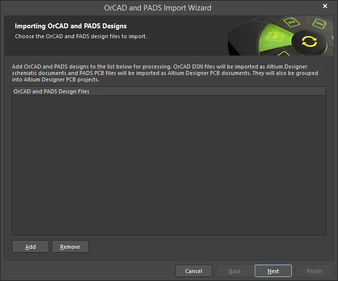
ウィザードのこのページを使用して、インポートする OrCAD および PADS 設計ファイルを追加します。Addをクリックして、目的のファイルを検索して選択します。Removeをクリックして、選択したファイルを削除します。
OrCAD and PADS Library Filesの選択
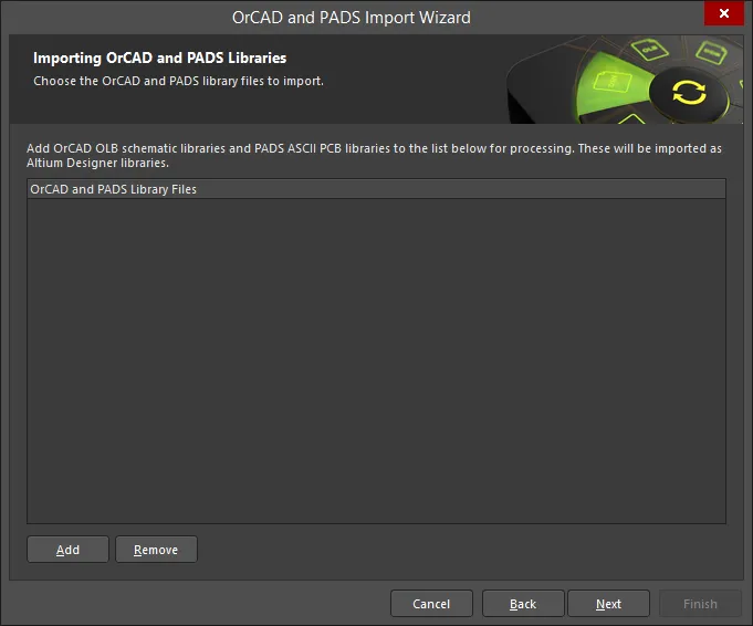
ウィザードのこのページを使用して、インポートする OrCAD および PADS ライブラリ ファイルを追加します。Addをクリックして、目的のファイルを検索して選択します。Removeをクリックして、選択したファイルを削除します。
Reporting Optionsの設定
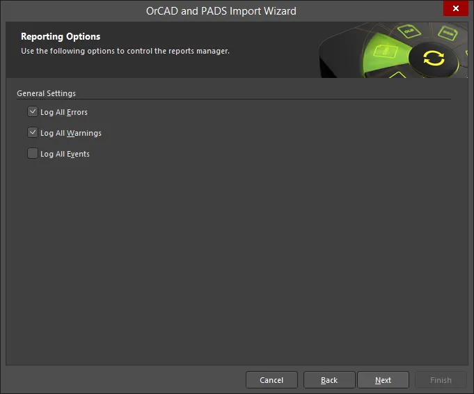
Reporting Optionsページを使用して、一般的なログ・レポート・オプションを設定します。
General Settingsで、必要なオプションLog All Errors、Log All Warnings、およびLog All Eventsを有効にします。
Schematic Optionsの設定
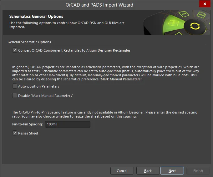
ウィザードのこのページを使用して、OrCAD DSN(設計)ファイルとOLB(ライブラリ)ファイルのインポート方法をコントロールします。
必要に応じて、Convert OrCAD Component Rectangles to Altium Designer Rectangles を有効にします。
通常、OrCAD プロパティは回路図パラメータ(配線プロパティを除く)としてインポートされ、テキストとしてインポートされます。回路図パラメータは、Auto-position Parametersを有効にすることで自動配置するように設定でき、回転やその他の移動後に邪魔にならない場所に自動的に配置されます。デフォルトでは、手動で配置されたパラメータは青いドットでマークされます。このデフォルトを無効にするには、Disable "Mark Manual Parameters" を有効にします。
OrCADのピン間スペーシング機能は、現在Altium Designerでは使用できません。Pin-to-Pin Spacingテキスト ボックスに目的の間隔比を入力します。入力した間隔に基づいてシートのサイズも変更する場合は、Resize Sheetを有効にします。
Schematic Sheet Optionsの設定

ウィザードのこのページを使用して、OrCAD ページとジャンクションのインポート方法を制御します。
OrCAD の表題欄は、回路図コンポーネントとしてインポートされます。Altium Designerもこの機能をサポートしています。ただし、Altium Designerの表題欄は、標準とANSIの2種類に制限されており、そのグラフィックは編集できません。これが状況にとって望ましくない場合は、テンプレートを使用して、より柔軟なソリューションを提供できます。テンプレートを使用すると、任意のグラフィックデータを回路図シートに配置できます。OrCAD 表題欄を剥がすには、Strip OrCAD Title Blocksを有効にします。必要に応じてEnable Schematic Title Blocksをオンにし、ドロップダウンを使用してStandardまたはANSIを選択します。
Force convert all I/O and Bi-directional pins to passive pinsを有効にすると、自動的に I/O に変換され、双方向ピンがパッシブ ピンに変換されます。
Default PCB and PCB Library Optionsの設定
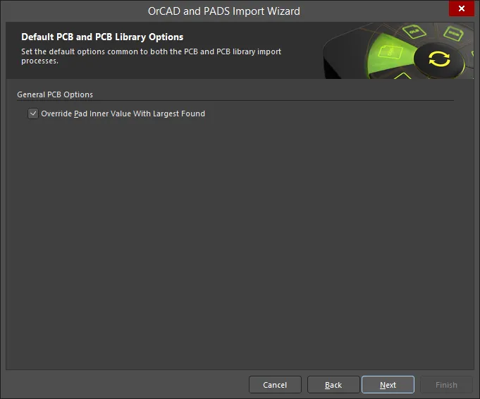
ウィザードのこのページを使用して、PCB と PCB ライブラリの両方のインポート プロセスに共通する既定のオプションを設定します。
Override Pad Inner Value With Largest Foundを有効にすると、読み込まれたパッドの中間レイヤーのサイズが見つかった最大サイズに設定されます。
Options for PCB Import Processの設定
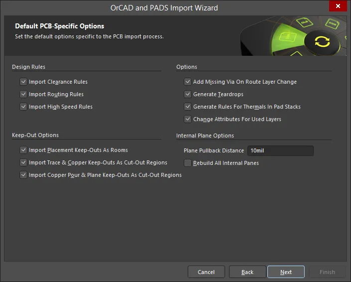
ウィザードのこのページを使用して、PCB インポート プロセスに固有の既定のオプションを設定します。
インポートするKeep-Out Options( Import Clearance Rules、 Import Routing Rules、およびImport Routing Rules) を有効にします。
必要なその他のオプションを有効にする:
- Add Missing Via On Route Layer Change
- Generate Teardrops
- Generate Rules For Thermals In Pad Stacks
- Change Attributes For Used Layers
テキストボックスで目的の Plane Pullback Distanceを指定します。Rebuild All Internal Planesのチェックボックスを有効にします。
PCB and PCB Library Options
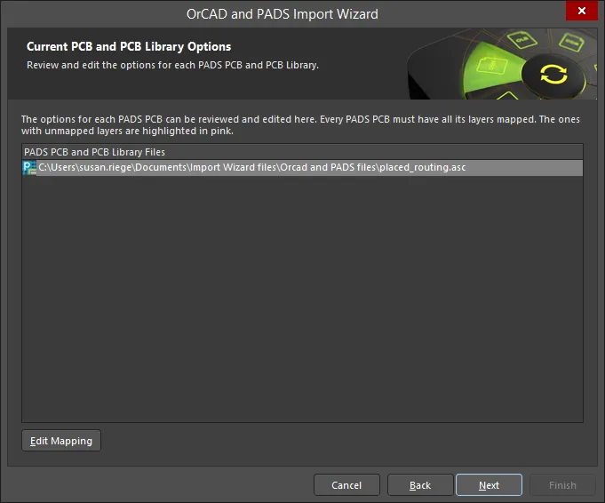
ウィザードのこのページは、各PADS PCBおよびPCBライブラリのオプションを確認および編集するために使用されます。マッピングされていないレイヤーはピンク色でハイライト表示されます。
Edit Mappingをクリックして、PADS PCB Library ASCII File Import Optionsダイアログを開きます。
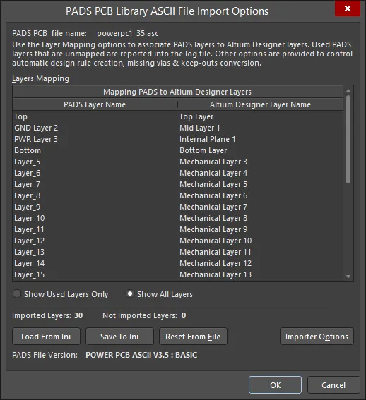
インポートする前に、使用するすべてのPADS PCBレイヤーをAltium Designerレイヤーにマッピングする必要があります。PADS PCB Library ASCII File Import Optionsダイアログでは、PADS PCBレイヤーをAltium Designerレイヤーにマッピングできます。また、このダイアログでは、インポート処理中にデザインルール、ビアの欠落、禁止の変換を制御できる Importer Settingsダイアログにもアクセスできます。
Output Library Optionsの設定
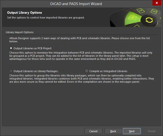
ウィザードのこのページを使用して、インポートされたライブラリのグループ化方法を制御します。
Library Import Options – 出力ライブラリーをグループ化する方法について、以下のオプションのいずれかを選択します。
- Output Libraries as PCB Project – 選択すると、PCBと回路図ライブラリ間の統合が最小限に抑えられます。インポートされたライブラリは、PCBプロジェクトとしてのみグループ化されます。これらは、後でライブラリパネルのライブラリのリストに追加できます。このセットアップは、OrCADで行っていたのと同じ環境で操作したい人にとって最も有利です。
- Output Libraries as Library Packages – ライブラリをライブラリパッケージにグループ化する場合に選択します。その後、Compile as Integrated Librariesを使用可能にすることにより、ライブラリー・パッケージを統合ライブラリーとしてコンパイルすることを選択できます。統合ライブラリは、PCB、回路図、PSpiceライブラリの両方を組み合わせて、より良い相互作用を可能にします。コンパイルのエラーは、Messagesパネルに表示されます。
Specifying the Output Directory
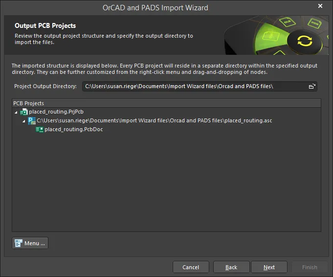
ウィザードのこのページを使用して、出力プロジェクトの構造を確認し、ファイルをインポートする出力ディレクトリを指定します。Browse Folderアイコンを使用して、Project Output Directoryを検索して選択します。
Menuをクリックして、プロジェクト構造を編集するためのオプションにアクセスします。
PCB Projects領域を右クリックすると、Menuボタンをクリックしたときと同じメニューとサブメニューにアクセスできます。
Specifying the Output Library Directory
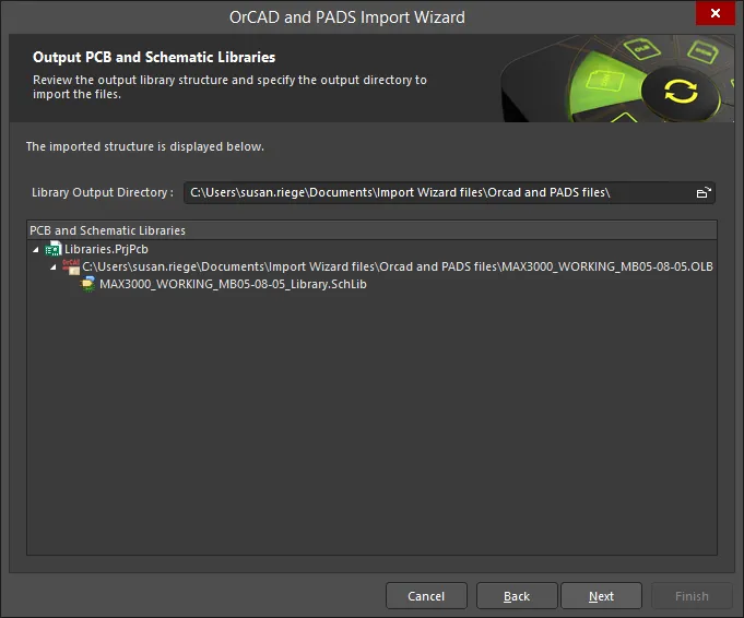
ウィザードのこのページを使用して、出力ライブラリの構造を確認し、ライブラリ ファイルをインポートする出力ディレクトリを指定します。Browse Folderアイコンを使用して、Library Output Directoryを検索して選択します。
Executing Import Process
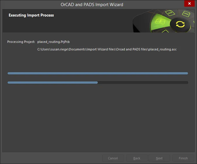
このページには、インポート処理の緑色の進行状況バーが表示されます。
Wizardの終了
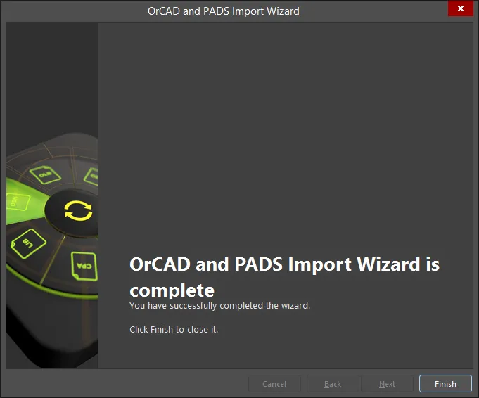
OrCAD と PADS のインポート ウィザードが完了しました。Messagesパネルに、関連するメッセージが表示されます。Finishをクリックしてウィザードを閉じます。インポート処理中に警告が生成された場合は、*.LOG ファイルが開き、警告が表示されます。
PADS と OrCAD ファイルは次のように変換されます:
- パッドASCII PCBレイアウト(
*.ASC) ファイルは Altium Designer の PCB ファイル (*.PcbDoc) です。
- PADSのASCII PCBライブラリファイルは、Altium DesignerのPCBライブラリファイル(
*.PcbLib) です。
- OrCADキャプチャ(
*.DSN)ファイルは、Altium Designerの回路図ファイルに変換されます。.DSNファイルは、単一のAltium Designer回路図ファイル(*.SchDoc です。内のデザイン キャッシュ。DSN ファイルは回路図ライブラリ (*.SchLib) です。複雑な階層を含む設計階層が維持されます。
- OrCAD回路図ライブラリ(
*.OLB)ファイルは、Altium Designerの回路図ライブラリファイル(*.SchLib) です。
- ファイルはAltium DesignerのPCBプロジェクト(
*.PrjPCB) が自動的に作成されます。
- 翻訳されたOrCADライブラリは、自動的に1つのPCBプロジェクトにグループ化されます。

 AI で翻訳