
PCBにおける接続性を理解する
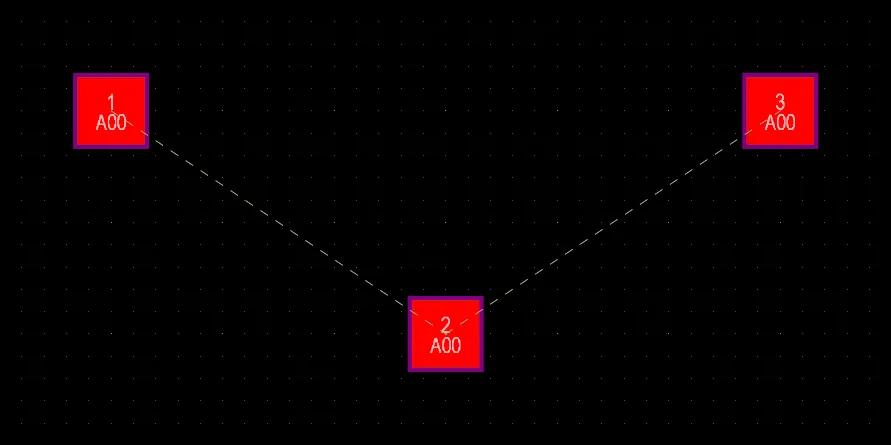
PCBエディタでは、ネット内のノード間の接続性は一連の点対点の接続ラインとして表され、これらを総称してラッツネスト(ratsnest)と呼びます。 設計が回路図(Design » Update PCB)から転送されると、コンポーネントがPCBの設計空間に配置され、接続ラインが(細い実線として)表示されます。
個々のネット内では、接続ラインがそのネット内のすべてのノードを結びます。どのようなパターン(順序)で接続されるかはNet Topologyと呼ばれ、discussed belowで説明します。
に従って接続ラインで結ばれます。")
ネット内のノードは、適用されるRouting Topologyルール(デフォルトはShortest)に従って接続ラインで結ばれます。

この設計では、GNDおよび5Vネットは接続ラインに別の色を使用しています。
接続ラインは、部品配置時の有用なガイドであるだけでなく、インタラクティブルーティングやオートルーティング時にも貴重なガイドとなります。
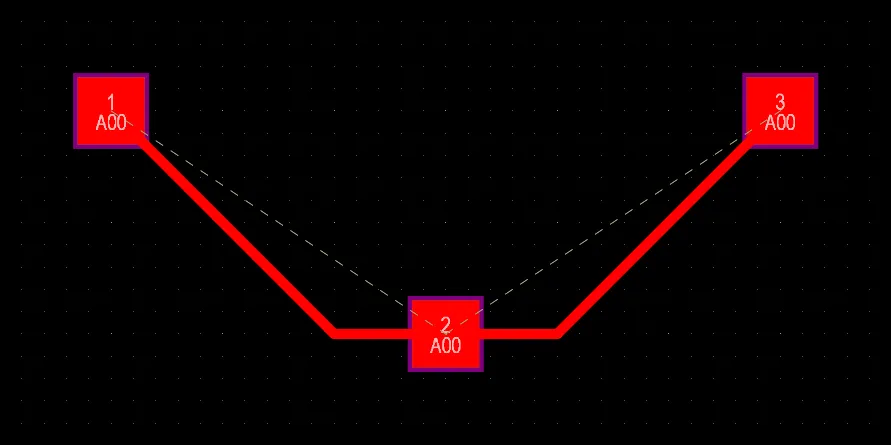
PCBエディタにはネットアナライザが含まれており、設計空間内のすべてのオブジェクトの位置を常時監視し、ネット種別のオブジェクトが編集された場合(オブジェクトの移動を含む)に接続ラインを更新します。たとえばコンポーネントを移動すると、そのコンポーネントからの各接続の遠端が、あるターゲットパッドから別のターゲットパッドへジャンプすることがあります。これは、適用される設計ルールで定義されたトポロジを維持するよう更新されるためです。下の動画ではGNDネットの例を示しています。 このネットのトポロジはShortestです。
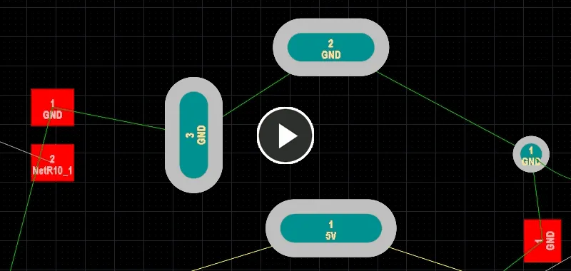
抵抗を移動するとGNDの接続ラインが飛び回り、全体の接続長が最短になるよう自動的に並べ替えられる点に注目してください。
基板上でネットを見つける
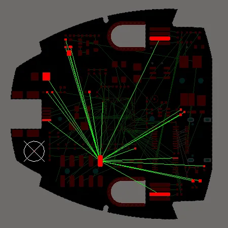
未配線の基板は、基板全体に接続ラインが交差する塊のように見えて圧倒されがちです。ルーティングの良い進め方は回路図から作業することで、重要なコンポーネントやクリティカルなネットを簡単に見つけられます。回路図のコンポーネントやネットから直接クロスセレクト/クロスプローブでき、PCB上の対応する項目がハイライトされます。詳細はWorking Between the Schematic and the Boardを参照してください。
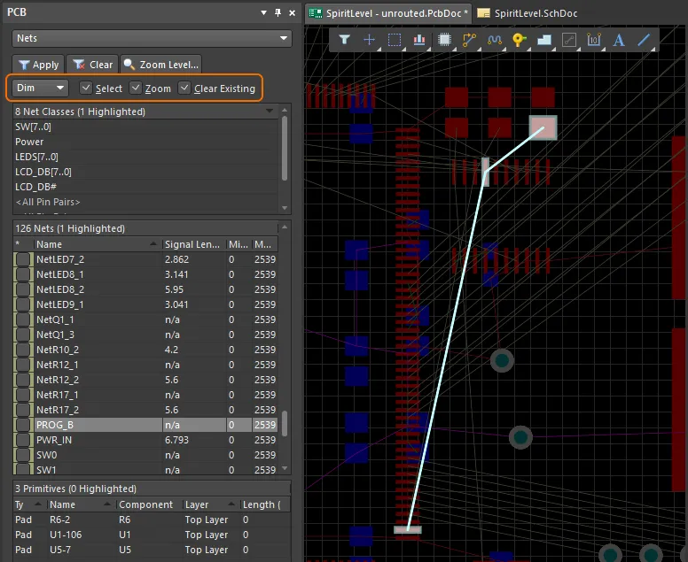
有用な機能として、PCBエディタには設計空間内のオブジェクトをマスクまたは減光できる機能があります。このフィルタリング機能は、フィルタを通過したオブジェクト以外をすべてフェードアウトします。下の画像は、単一のネットが選択され、フィルタリングシステムがDim(フィルタを通過しないすべてのオブジェクト)に設定されている例です。
これを試すには、PCB panelをNetsモードに設定します。これにより基板上のネット一覧が表示されます。ドロップダウンでフィルタモードをDimまたはMaskに設定し、次に下の画像のようにSelectおよびZoomオプションを有効にします。
パネルでネット名をクリックすると、設計空間の表示が変化し、そのネット内のノードが見えるようにズームし、ネット内のパッドと接続ライン以外はすべてフェードアウトします。つまり、そのネットだけを基板の他の部分から“引き出す”ように表示できます。ワークスペースをクリックしてもフィルタは維持され、選択したネットが明瞭に表示されたままなので、確認やルーティングが容易になります。
フィルタ機能を使うと、ネットやネットクラスを見つけやすくなります。
PCBパネル上部のClearボタンをクリックしてフィルタをクリアし、設計空間全体を通常の明るさに戻します(またはShift+Cショートカットを押します)。
個別ネットだけでなく、パネルのNet Classesセクションで(クラスが定義されている場合)ネットクラスをフィルタすることもできます。また、複数のネットをインタラクティブに選択することも可能です(PCBパネルでネット名をクリックする際にCtrl を押し続けます)。
 )
)ネットの参照
PCB panel's Netsモードでは、3つの主要領域が現在のPCB設計のネット階層を反映するように変化します(上から順に):
-
Net Classes基板で定義された
。 - クラス内の個々のメンバーNets 。
- ネット内の個々のPrimitives (パッド、ビア、配線、フィル)。
ネットクラス
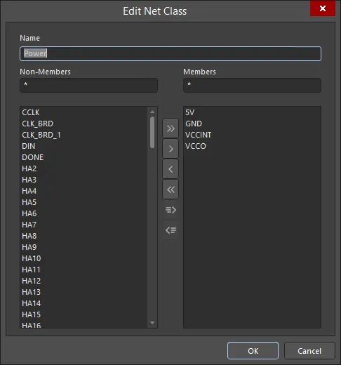
パネル上部領域(Net Classes)で、ネットまたはネット項目のエントリを右クリックして、表示されるメニューからProperties を選択(またはエントリを直接ダブルクリック)すると、Edit Net Class dialog にアクセスできます。ここで、クラスのネット所属の表示/編集、名称変更、追加クラスの作成が行えます。
また、メインメニューのDesign » Netlistサブメニュー、または選択したネットオブジェクトの右クリックメニューのNet Actions サブメニューにある次のコマンドでもネットクラスを管理できます。
- Create NetClass from Selected Nets - このコマンドは、設計空間で選択した2つ以上のネットから新しいネットクラスを作成するために使用します。 コマンドを起動するとObject Class Nameダイアログが開きます。ここで新しいNet Classに必要な名前を指定します。OKをクリックするとネットクラスが作成され、選択したネットがメンバーとして追加されます。
- Add Selected Net(s) to NetClass - このコマンド は、選択した1つ以上のネットを既存のネットクラスに追加するために使用します。 コマンドを起動するとChoose Net Classダイアログが開きます。このダイアログには既存のネットクラスがすべて一覧表示されます。対象クラスを選択してOKをクリックすると、ネットがそのクラスのメンバーとして追加されます。
- Remove Selected Net(s) From NetClass - このコマンド は、選択した1つ以上のネットを既存のネットクラスから削除するために使用します。 コマンドを起動するとChoose Net Classダイアログが開きます。このダイアログには既存のネットクラスがすべて一覧表示されます。対象クラスを選択してOKをクリックすると、ネットはそのクラスのメンバーから削除されます。
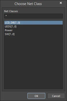
Choose Net Classダイアログ
ネット
パネル中央の領域には、上の領域で選択したNet Class(複数可)に属するネットが表示されます。
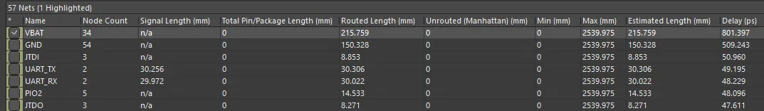
デフォルトでは、各ネットに対して次の情報が一覧表示されます。
-
 - この機能には2つの役割があります:
- Color background - ネットに割り当てられた色。この色は常にネットの接続ラインに適用されます。また、ネットカラー表示オーバーライド機能を使用して、そのネットの配線にも適用できます。ダブルクリックでこのネットの色を編集するか、右クリックで現在選択中のすべてのネットの色を編集します。
-
checkbox - これをチェックすると、このネットの配線に色を適用します(ネットカラー表示オーバーライド機能を有効化)。右クリックで、現在選択中のすべてのネットに対して表示オーバーライド機能を有効(または無効)にできます。F5を押すと、設計空間でネットカラー表示オーバーライドを有効/無効に切り替えられます。
► 詳細はNet Color Override - Displaying the Net Color on Routed Netsを参照してください。
-
Name - ネット名。
-
Node Count - このネット内のパッド総数。
-
Routed Length - ルーティングを構成する配置済みのトラックおよびアークセグメントの長さの合計に、ビアを通って移動する垂直距離を加えたもの(下記注記参照)。配線長計算では、重なり合うトラックセグメントやパッド内の配線のうねり(wiggles)を解決しようとはしません。
-
Signal Length - ノード間の総距離を高精度に計算します。配置済みオブジェクトを解析して、積層/重なり合うオブジェクトやパッド内の回り込み経路を解決し、ビア長も含めます。ネットが完全に配線されていない場合は、接続ラインのマンハッタン長(X + Y)も含めます。
信号長(Signal Length)計算には次の注記が適用されます:
-
パッド内部の重なりや蛇行(ウィグル)を解消します。
-
トラックやアーク以外のオブジェクト(例:リージョンやフィル)で作成された配線パスにも対応します。
-
ビアを介した垂直方向の距離を含みます(下記注記参照)。
-
このネットの Total Pin/Package Length を含みます。
-
このネットの Unrouted (Manhattan) 長を含みます。
-
適用される Length/Matched Length デザインルールに準拠していない場合、信号長が色付き背景で表示されてフラグされます。短すぎる信号長は黄色、長すぎる信号長は赤で表示されます。
► Length および Matched Length デザインルールがどのように適用されるかの詳細は、Length Tuning を参照してください。
-
信号はポイント・ツー・ポイントのエンティティです。このため、パネルの Nets モードで Signal Length が表示されるのはノードが2つのネットのみです(ノード数が異なるネットでは
0が表示されます)。ノードが2つを超えるネットについては、xSignals を定義して信号長を算出してください。► PCB - xSignals を参照してください。
► xSignals の詳細は、Defining High Speed Signal Paths with xSignals を参照してください。
-
-
Total Pin/Package Length - 当該ネット内のすべてのパッドに設定された Pin Package Length 値の合計。この値は PCB パッドのプロパティとして定義され、回路図のピンでも指定できます。
-
Unrouted (Manhattan) - 未配線区間すべての垂直+水平(X+Y)距離。
領域内で右クリックし、Columns サブメニューを使用して次の列を追加します:
-
Min/Max - 適用される Length および Matched Length デザインルールの設定。適用ルールが定義されていない場合は、
Min=0milとMax=99999milの内部デフォルトが使用されます。► Min と Max の設定が Length および Matched Length デザインルールからどのように導出されるかの詳細は、Length Tuning を参照してください。
- Estimated Length - これは Routed Length に、まだ配線されていない区間の接続線の長さを加えたものです。未配線部分については Manhattan 長は使用せず、代わりにポイント・ツー・ポイントの直線距離を使用します。
- Delay - 信号がその配線に沿って伝搬するのに要する時間。
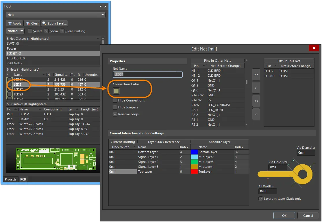
Nets 領域内の特定ネットのエントリをダブルクリック(またはネットのエントリを右クリックしてコンテキストメニューから Properties コマンドを選択)すると、Edit Net ダイアログが開き、ネットのプロパティを変更できます。
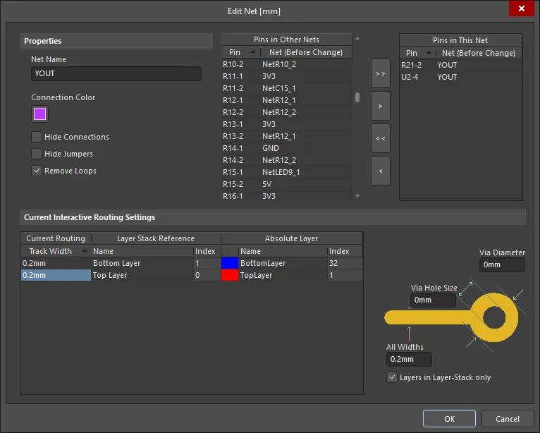
Options and Controls of the Edit Net Dialog
プロパティ
- Net Name - 必要に応じてネット名を変更します。
- Connection Color - クリックして Choose Color ダイアログを開き、指定ネットの接続色を選択します。このネット色は、Net Color Override 機能が有効な場合(F5 を押す)、配線済みネットにも適用できます。
- Hide Connections - 有効にすると接続ワイヤを非表示にします。
- Hide Jumpers - 有効にすると、ジャンパーまたは配線済みセグメント間の短い接続を非表示にします。
- Remove Loops - 有効にすると、このネットに含まれる冗長なループを自動的に削除します。
他のネットのピン
PCB 上のすべてのピンの一覧です。現在ネットに割り当てられているピンは、角括弧内にネット名が表示されます。編集対象ネットに追加したいピンを選択します。複数ピンの選択には Shift および Ctrl キーを使用します。コントロールボタンで選択したピンを現在のネット一覧へ移動するか、右クリックしてコンテキストメニューから選択ピンを一覧から削除します。
ボタン
-
 - すべての Pins in Other Nets を Pins in This Net に追加します。
-
 - 選択した Pins in Other Nets を Pins in This Net に追加します。 複数ピンの選択には Shift および Ctrl キーを使用します。
-
 - すべての Pins in This Net を Pins in Other Nets に移動します。
-
 - 選択した Pins in This Net を Pins in Other Nets に移動します。 複数ピンの選択には Shift および Ctrl キーを使用します。
Pins in Other Nets リストから Pins in This Net リストへピンを移動した後、移動したピンを右クリックして Remove One コマンドを選択すると、Pins in Other Nets リストへ戻せます。
このネットのピン
このネット内のすべてのピンを一覧表示します。このネットから削除したいピンを選択します。複数ピンの選択には Shift および Ctrl キーを使用します。コントロールボタンで選択したピンを現在のネット一覧から外すか、右クリックしてコンテキストメニューで選択ピンを削除します。
現在のインタラクティブルーティング設定
グリッド
グリッド領域には、インタラクティブルーティングの現在設定が一覧表示されます。
- Track Width - 現在のインタラクティブルーティング設定のトラック幅フィールドを一覧表示します。編集可能で、好みや設計要件に合わせて変更できます。
- Name - Current Routing、Layer Stack Reference、Absolute Layer を一覧表示します。
- Index - インデックス番号を一覧表示します。
図
- Via Hole Size - これはネットに保存されている、現在のビア穴サイズのユーザー選択値を表します。このダイアログでは、現在のインタラクティブルーティング設定の値を変更できます。値が 0 の場合、ユーザー選択値はこのダイアログから取得されず、このボードで最後に使用した値が使用されます。
- Via Diameter - これはこのネットに保存されている、現在のビアサイズのユーザー選択値を表します。このダイアログでは、現在のインタラクティブルーティング設定の値を変更できます。値が 0 の場合、ユーザー選択値はこのダイアログから取得されず、このボードで最後に使用した値が使用されます。
- All Widths - これは現在の配線およびそのレイヤ参照値で、ネットに保存されている現在のユーザー選択値を表します。現在のインタラクティブルーティング設定の値を変更する手段を提供します。値が 0 の場合、ユーザー選択値はこのダイアログから取得されず、このボードで最後に使用した値が使用されます。
- Layers in Layer-Stack only - 有効にすると、レイヤスタック内のレイヤに対してのみビアパラメータを適用します。
プリミティブ
パネル下部の Primitives 領域における各ネット項目タイプの表示/含めるかどうかは、Nets または Primitives 領域からアクセスできる右クリックメニューで、各項目に対応するオプションが有効になっているかどうかに依存します。

ネットまたはネット項目のエントリを右クリックして、含める項目を選択します。
Primitives リストの右クリック・コンテキストメニューには、選択した2つの項目間に xSignal を作成するオプションもあります。詳細は PCB - xSignals を参照してください。
接続線表示の管理
Related page: PCB の表示
接続線は、部品の配置や向きの調整を助け、配線時のガイドにもなる有用な補助です。一方で、表示が煩雑になる原因にもなります。これに対処するため、PCB エディタには、設計者が接続線の表示を管理できるよう、以下に示す機能が用意されています。
接続線の色を変更する
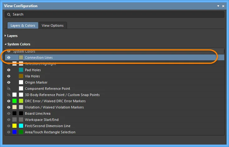
回路図から PCB ワークスペースへ設計を転送すると、デフォルトのレイヤおよび色設定が適用されます。この処理の一環として、すべての接続線には、View Configuration パネル(L ショートカット)の Layers & Colors タブ内 System Colors セクションで定義されたデフォルトの Connection Lines 色が割り当てられます。ビュー構成は 2D/3D の両ワークスペースで使用でき、保存して再適用できます(View Configuration パネルの View Options タブ)。
配線作業中に重要なネットを目立たせる簡単な方法は、接続線の色を変更することです。これを行うには、PCB パネルでネット名をダブルクリックして Edit Net ダイアログを開き、接続線の色を編集します(パネルを Nets モードに設定)。
または、複数ネットのうち or 1つの色を変更するには、まず PCB パネルで必要なネットを選択し、選択したネット上で右クリックして Change Net Color コマンドを選択します。

PCB パネルで選択したネットを右クリックし、接続線の色を変更します。
レイヤ色を使用して接続線を表示する
個々のネットに対して接続ラインの色を割り当てるだけでなく、接続ラインが通過する開始層と終了層の色を使って接続ラインを表示することもできます。接続ラインがある層上のオブジェクトから別の層上のオブジェクトへ移動する場合、接続は最初のオブジェクトがある層の色で始まり、もう一方の層上のオブジェクトに近づくにつれて、終点側の層の色へと変化します(下の画像のとおり)。
この機能は多層基板を配線する際に、配線中の接続が向かうべきターゲット層を示してくれるため便利です。色の変化(モーフィング)は、ある層から別の層へ移動する接続にのみ適用されます。接続の開始と終了が同じ層の場合は、割り当てられたネット色のままです。
層の色機能を使用するには、View ConfigurationsパネルのView OptionsタブでUse Layer Colors for Connection Drawingオプションを有効にします(下図参照)。

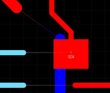
接続ラインは開始層と終了層の色を使って表示できます。右の画像では、接続ラインの表示方法が分かるように、いくつかのネットで配線セグメントを削除しています。
単一層モードでの接続ライン表示
多層基板は視覚的に情報が密で、状況を把握しにくくなります。これを補助するため、有効な層の表示から単一層モードへ、Shift+Sショートカットを押すだけで簡単に切り替えられます。
通常この操作を行うと、現在の層で開始も終了もしない接続ラインは、関連がないと見なされて非表示になります。常に接続ラインを表示するには、View ConfigurationsパネルのView OptionsタブでAll Connections in Single Layer Modeオプションを有効にします(下図参照)。

単一層モードでの接続ライン表示を制御します。
接続ラインの非表示/表示
PCBパネルでネットをフィルタリングする代替として、1本、複数、またはすべての接続ラインを完全に非表示にすることもできます。接続ラインの表示を制御するコマンドがView » Connectionsサブメニューに用意されています。作業中にNショートカットキーを押して、これらのコマンドへアクセスすることもできます。 利用可能なコマンドで次を実行できます:
ネットトポロジ
ネット内のノード同士がどのようなパターン/順序で接続されるかを、ネットトポロジと呼びます。ネットトポロジは該当するRouting Topologyデザインルールで制御され、デフォルトは Shortest トポロジです。Shortest とは、そのネットの接続総延長が最短になるようなパターンでノード同士を接続することを意味します。この総延長はコンポーネント移動中に監視され、総延長が最短になるように接続ラインのパターンが動的に変化します。これは上のアニメーションで確認でき、移動中のコンポーネント下側から下方向へ伸びる接続ラインが、コンポーネントの移動に伴って跳ねるように変化します。これは、接続されているパッドのいずれかが同一ネット内の別のパッドに近づくたびに発生します。
Routing Topology デザインルールを使用して事前定義トポロジを適用する
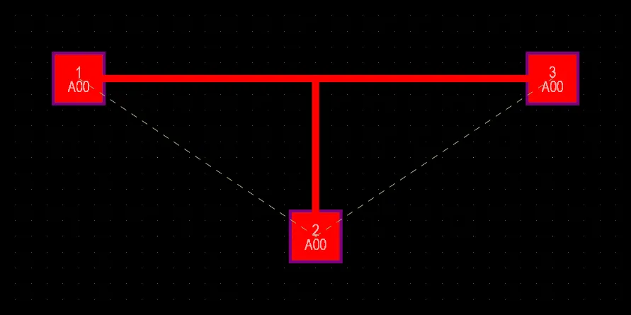
追加のRouting Topology design rulesを作成して、ネット(またはネットクラス)に別のトポロジを使用させることができます。これを示すため、下の画像では左にデフォルトのトポロジルール、右に同じネットへ Starburst の新しいルーティングトポロジを適用した例を示しています。Starburst トポロジでは、Electrical TypeがSourceのパッド(すべてのパッドのデフォルトタイプは Load)から接続が放射状に広がります。

デフォルトトポロジでは、接続総延長が最短になるように接続ラインが配置されます。Starburst トポロジでは、接続ラインはすべて Source パッドから放射状に広がります。
カスタムトポロジの適用
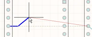
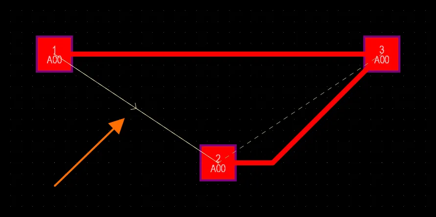
個々のネット内で、2つのノード間の接続は From-To と呼ばれます。ピン間レベルで接続ラインの経路を制御するには、ネット内に From-To を手動で定義し、実質的にカスタムのネットトポロジを作成できます。
From-To は、PCB panel をFrom-To Editorモードに設定して定義します。From-To を定義する手順は、パネル内で2つのNodes on Netを選択し、Add From Toボタンをクリックします。設計空間で From-To を明確に識別できるよう、From-To は実線ではなく破線で表示されます。

2つのパッド間に From-To が定義されています。From-To ラインが実線ではなく破線で表示されている点に注目してください。
PCBパネルのFrom-To Editorモードは3つのセクションに分かれています:
- Nets
- Nodes選択したネットの
- From-Tos on Net
ネットのエントリをクリックすると、そのネット上のすべてのノードがパネル中央の領域に読み込まれます。ネットのエントリをダブルクリックするとEdit Net dialog が開き、ノードの所属を含むネットのプロパティを編集できます。
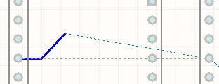
From-To の追加
選択したネット内の2つのノード間にユーザー定義の From-To を追加するには、パネルのNodes on Net領域で2つのノードを選択し、Add From Toボタンをクリックします。
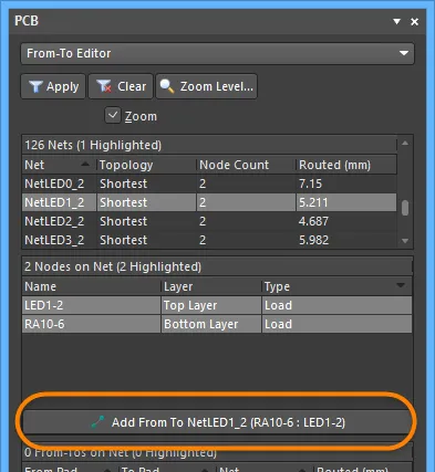
新しく追加された From-To はパネルのFrom-To on Net領域に一覧表示され、設計空間では2つのノード間の点線として表示されます。

ネット上に新しい From-To が作成されました。

設計空間内のユーザー定義 From-To。
From-To を削除するには、パネルのFrom-To on Net領域で該当エントリを選択し、Removeボタンをクリックします。
事前定義トポロジの選択
ネットのトポロジとは、ピン間接続の配置またはパターンのことです。デフォルトでは、各ネットのピン間接続は接続総延長が最短になるように配置されます。
トポロジはさまざまな理由でネットに適用されます。たとえば高速設計で信号反射を最小化する必要がある場合はデイジーチェーン・トポロジでネットを構成します。GND ネットでは、すべての配線が共通点へ戻ることを保証するためにスター・トポロジを適用することがあります。ネット内のノードペアに対して専用の From-To を作成することも、利用可能な事前定義ルーティングトポロジのいずれかに基づいて、そのネットの From-To を生成することもできます。
次のトポロジが利用可能で、パネルのFrom-To on Net領域からGenerateボタンをクリックしてアクセスできます:
- Shortest - このトポロジは、ネット内のすべてのノードを接続し、接続総延長が最短になるようにします。
-
Daisy Simple- このトポロジは、すべてのノードを順番に(1つずつ)連結します。連結する順序は、全体の長さが最短になるように計算されます。ソース・パッドと終端(ターミネータ)パッドが指定されている場合、他のすべてのパッドはそれらの間に、可能な限り最短となるように連結されます。複数のソース(またはターミネータ)が指定されている場合、それぞれの端で互いに連結されます。
-
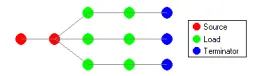
Daisy Balanced - このトポロジは、すべての負荷(Load)を等しいチェーンに分割し、チェーンの総数はターミネータの数と同じになります。これらのチェーンは、その後スター(星形)パターンでソースに接続されます。複数のソース・ノードは互いに連結されます。
-
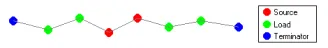
Daisy Mid-Driven - このトポロジは、ソース・ノードをデイジーチェーンの中央に配置し、負荷を均等に分割して、ソースの両側へチェーン接続します。終端は2つ必要で、各端に1つずつ必要です。複数のソース・ノードは中央で互いに連結されます。ターミネータがちょうど2つでない場合は、Daisy-Simple トポロジが使用されます。
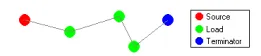
- Starburst - このトポロジは、各ノードをソース・ノードへ直接接続します。ターミネータが存在する場合は、各負荷ノードの後に接続されます。複数のソース・ノードは、Daisy Balanced トポロジと同様に互いに連結されます。
パッドは、Electrical Type フィールドの項目を適切に変更することで、Source/Terminator/Load として定義できます。これは、Properties パネルの Pad モード内で行います。Properties パネルの Pad モードへは、Nodes on Net 領域で該当パッドの項目をダブルクリックしてアクセスします。

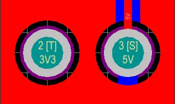
Properties パネルの Pad モードで、パッドの Electrical Type を Source に設定している例。
パッドの電気タイプを Source または Terminator に変更すると、区別のためにデザインスペース上に「[S]」または「[T]」が配置されます。
注記
-
システム生成の接続ラインは、デザインスペース上で独立した別エンティティとしては表示されません。表示されるのは、From-To に関連付けられたピン間(pin-to-pin)の接続ラインのみで、これはインタラクティブルーティング/オートルーティングのガイダンスに使用されます。
-
ユーザー定義の From-To は、デザインスペース上に点線として表示され、同時に表示されるピン間接続ラインとは別個のものとして明確に区別されます。ユーザー定義の From-To ラインは、関連するピン間接続ラインの開始点と終了点を制御します。これは例で示すのが最も分かりやすいでしょう。論理的に接続された2つのコンポーネントのピン間にユーザー定義 From-To を追加した場合を考えます。接続ラインも追加され表示されます(PCB パネルを Nets モードに設定):
-
ルーティング用途に使われるピン間接続ラインが、明確に別物であるユーザー定義 From-To ラインの存在を覆い隠します。しかし、接続のルーティングを開始すると、2本のラインが別個であることが確認できます。
-
ここでルーティングを中断すると、ネットアナライザが必要なトポロジを維持するために接続ラインを追加します。これは点線(Broken Net Marker と呼ばれる)で表示され、ユーザーがユーザー定義 FromTo を追加することで決定したトポロジを維持するために、ネットをこの2点間で配線すべきことを示します。
-
ネットの一部にのみユーザー定義 From-To を指定した場合、PCB エディタは残りのピン間接続(システム生成 From-To)を Shortest トポロジに設定します。
-
From-To の種類によって、たとえばネットオブジェクトを移動した場合や、ネットの一部を手動で配線した場合に、Connectivity Analyzer がデザインスペース上の接続ラインをどのように扱うかが決まります。
- System-generated From-To - 接続ラインは、ネットアナライザがネットのデフォルトトポロジ(つまり Shortest)を維持するために行う再最適化の一部として、必要に応じて移動されます。
- User-defined From-To - From-To が事前定義トポロジの選択結果ではない場合、接続ラインはネットアナライザの再最適化プロセスの一部とは見なされません。From-To が(Shortest 以外の)事前定義ネットトポロジの一部である場合、選択したトポロジが維持される限り、ネットアナライザは再最適化にそれを含めることができます。
-
From-To を用いて定義したカスタムトポロジの実装は、対応するネットに適用された Routing Topology デザインルールの Batch Design Rule Check (DRC) で確認できます。From-To のパッド間に電気的接続があり、かつ最短経路にこのネットの別のパッドが少なくとも1つ含まれる場合、違反が検出されます。
3つのパッド間に2つの From-To が作成されます(パッド1→パッド2、およびパッド2→パッド3)
From-To の設定に従って配線が作成されます。パッド1と2の間、およびパッド2と3の間に配線があり、Routing Topology ルールの違反は検出されません。
T分岐(T-branch)形状で配線が作成されます。From-To 設定に基づく経路に追加のパッドは存在しないため、Routing Topology ルールの違反は検出されません。
パッド1とパッド3の間、およびパッド2とパッド3の間に配線が作成されます。この配線は From-To 設定と一致しません。パッド1とパッド2の経路に追加のパッド3が含まれるため、パッド1と2の間の From-To に対する Routing Topology ルール違反が検出されます。
Netlist Manager
メインメニューから Design » Netlist » Edit Nets コマンドを選択して開く Netlist Manager ダイアログには、基板のネットリストを効果的に管理するためのコントロールが用意されています。必要に応じてネットの追加、編集、削除ができ、これらのネットに含まれるコンポーネントのピン(またはパッド)についても、プロパティに関して編集できます。また、このダイアログから他のネットリスト管理ツールにもアクセスでき、PCB 上の接続された銅箔に基づいてネットリストを作成する機能や、PCB からネットリストをエクスポートする機能も含まれます。
 Netlist Manager ダイアログ
Options and Controls of the Netlist Manager Dialog
-
Nets In Board - このダイアログ領域には、基板に定義されているすべてのネットが名前で表示されます。リスト上部のマスクフィールドを使用して、内容を素早くフィルタできます。
- Edit - クリックすると Edit Net dialog にアクセスできます。ここで、現在選択されているネット(または、リストで複数ネットが選択されている場合はフォーカスされているネット。フォーカスされているネットは点線の枠で表示されます)のプロパティを表示・変更できます。
- Add - クリックすると基板に新しいネットを追加します。Edit Net ダイアログが開き、ネットのプロパティを定義できます。新規ネットの初期デフォルト名は NewNet です。必要に応じて変更してください。
-
Delete - クリックすると、現在選択されているネットを基板から削除します。確認ダイアログが表示されるので、削除を続行するには Yes をクリックします。
-
Pins In Focused Net - この領域には、現在選択/フォーカスされているネットに関連付けられた(属する)すべてのピン(コンポーネント・パッド)が表示されます。リストの各項目では、ピンの識別子が <ComponentDesignator>-<PinDesignator> 形式で表示されます。リスト上部のマスクフィールドを使用して、内容を素早くフィルタできます。
- Edit - クリックすると Pad dialog にアクセスでき、現在選択されているピン(パッド)のプロパティを表示・変更できます。
-
Menu - クリックすると、次のコマンドを提供するメニューにアクセスできます。
- Add Net - 基板に新しいネットを追加するために使用します。Edit Net ダイアログが開き、ネットのプロパティを定義できます。
- Delete Net - 現在選択されているネットを基板から削除するために使用します。確認ダイアログが表示されるので、削除を続行するには Yes をクリックします。
-
Update Free Primitives From Component Pads - 配線プリミティブのネット名を、それらが接続しているパッドのネット名に再同期するために使用します。コマンドを起動すると、フリーなプリミティブのネットをコンポーネント・パッドのネットで更新するかどうかを確認するダイアログが表示されます。Yes をクリックすると、各パッドを起点に接続されている銅箔が選択され、各プリミティブのネット名がパッドのネット名に一致するように設定されます。
- Clear All Nets - 現在の設計ドキュメントからすべてのネットをクリアし、内部PCBネットリストを実質的に消去します。ソースの回路図ドキュメントでネット情報を変更し、PCBをソース回路図のネットリスト情報と完全に再同期したい場合に有用です。コマンドを起動すると、この操作によりPCBからすべてのネット情報がクリアされることを通知する確認ダイアログが表示されます。Yes をクリックすると、すべてのネット情報が削除されます。配線済みのトラックは配線されたまま残りますが、No Net の割り当てになります。未配線の論理接続は削除されます。
- Export Netlist From PCB - 現在のドキュメントの内部PCBネットリストをファイルにエクスポートするために使用します。コマンドを起動すると、PCBからネットリストをエクスポートするかどうかを確認するダイアログが表示されます。Yes をクリックすると、ネットリスト(Exported <PCBDocumentName>.Net)がPCB設計ドキュメントと同じフォルダに作成されます。
-
Create Netlist From Connected Copper - 現在の設計で配線によって作成された接続性に基づいてネットリストファイルを作成するために使用します。コマンドを起動すると、PCB上の銅箔からネットリストを生成するかどうかを確認するダイアログが表示されます。Yes をクリックすると、ネットリスト(Generated <PCBDocumentName>.Net)がPCB設計ドキュメントと同じフォルダに作成され、メイン設計ウィンドウでアクティブなドキュメントとして自動的に開きます。
Options and Controls of the Pad Dialog

Pad ダイアログ
Pad Template
- Template - ドロップダウンからPadテンプレートを選択します。
- Library - Padテンプレートがリンクされているライブラリを表示し、そのライブラリからテンプレートのリンクを解除するオプションも含まれます。
Location
- X - 現在の原点に対する、パッド中心の現在のX位置です。値を編集して、原点に対するパッド位置を変更します。
- Y - 現在の原点に対する、パッド中心の現在のY位置です。値を編集して、原点に対するパッド位置を変更します。
- Rotation - パッドの現在の回転角(度)です。編集してパッドの回転を変更します。最小角度分解能は 0.001° です。
Hole Information
- Hole Size - パッドの現在の穴サイズです。この値は、製造時にパッドにドリル加工される穴の直径(mil または mm)を指定します。SMDパッドやエッジコネクタのような単層パッドの場合、これは自動的に 0 に設定されます。穴サイズは 0~1000mil の範囲で設定でき、パッド領域より大きく設定して銅なしの機械穴を定義することもできます。このフィールドの値を編集してパッド穴サイズを変更します。値は mm または mil のいずれでも入力できます。
- Tolerance - 穴公差属性を設定すると、基板のはめあいと限界の判断に役立ちます。設計の穴公差の最小(-)および最大(+)を指定します。
穴の形状を指定するには、次のオプションのいずれかを選択します。
- Round - パッドの穴形状を丸穴(デフォルト)に指定します。
- Square - パッドの穴形状を角穴(打ち抜き)に指定します。
- Slot - パッドの穴形状を両端が丸い長穴(スロット)に指定します。
- Plated - このオプションは、パッドがめっき穴かどうかを決定します。設計内にめっきパッドと非めっきパッドの両方が存在する場合、非めっき穴はNCドリルファイルでめっき穴とは異なるツールを使用するように設定されます。
Properties
- Designator - 現在のパッドデジグネータです。パッドがコンポーネントの一部である場合、デジグネータは通常、対応するコンポーネントのピン番号に設定されます。デジグネータは最大20文字で、スペースは含められません。フリーパッドはデジグネータを含めることもできますし、このフィールドを空のままにすることもできます。デジグネータが数字で始まる、または数字で終わる場合、複数のパッドを連続して配置すると数字が自動インクリメントされます。このフィールドの値を編集してパッドデジグネータを変更します。必要に応じて、同一コンポーネントフットプリント内の複数パッドで同じデジグネータを共有できます。
-
Layer - パッドが現在割り当てられているレイヤです。パッドは利用可能な任意のレイヤに割り当てられます。Layer を
Multi-Layerに設定すると、すべての信号レイヤ上にパッド形状を定義します。 - Net - パッドが現在割り当てられているネットです。フィールドをクリックしてドロップダウンリストからネットを選択し、ネット割り当てを変更します。No Net を選択すると、パッドがどのネットにも接続されていないことを指定します。Net プロパティは、Design Rule Checker がPCBオブジェクトが適正に配置されているかを判断するために使用します。
- Electrical Type - このフィールドはパッドの現在の電気的ステータスを表示します。このステータスはコンポーネントパッドにのみ関連し、これらのパッドの伝送線路特性を設定します。パッドは Load、Source、Terminator として指定できます。Source と Terminator の設定は、ネットがデイジーチェーン配線トポロジのいずれかを必要とする場合に使用されます。フィールドをクリックして、ドロップダウンリストから電気タイプを変更します。
- Pin/Pkg Length - Pin Package Length は、Signal Length の計算に自動的に含まれ、その結果は PCB パネルに表示されます。選択したネット内のピンの Pin/Pkg Length の値を確認(または編集)するには、PCB パネルを Nets モードに設定します。
- Jumper ID - このパッドがジャンパーコンポーネントのフットプリントの一部であることを示すには、0以外の値(範囲 1~1000)に設定します。ジャンパーコンポーネントは、片面PCBで、トラックで接続を作る代わりにワイヤリンクで物理的にパッド同士を接続する場合に使用できます。Jumper ID の値は、どのパッドを「接続されている」として扱うかをソフトウェアに指示します。ジャンパー接続は同一コンポーネントフットプリント内のパッド間でのみ作成でき、同じ Jumper ID 値で、かつ同じネットに割り当てられている必要があります。さらに、コンポーネントの Type が Jumper に設定されている必要があります。これらの条件が満たされると、ジャンパー接続はPCBエディタで曲線の接続ラインとして表示されます。
- Locked - 有効にすると、パッドをグラフィカル編集から保護します。位置やサイズが重要なパッドはロックしてください。ロックされたプリミティブを編集しようとすると、そのプリミティブがロックされていることが通知され、操作を続行するかどうかを尋ねられます。このオプションがオフの場合、確認なしで自由に編集できます。なお、Locked チェックボックスはコンポーネントに属するパッドには影響しません。コンポーネントがロックされていない場合、コンポーネントを移動するとパッドも移動します。この状況では、誤操作による移動を防ぐためにコンポーネントをロックしてください。
Testpoint Settings
この領域では、このパッドを Fabrication および/または Assembly のテストポイントファイル生成用のテストポイントとして定義します。テストポイントとは、テストプローブがPCBに接触して基板の機能が正しいかを確認できる位置です。必要な Testpoint Type と Layer のチェックボックスを有効にすることで、任意のパッドまたはビアをテストポイントとして指定できます。これを行うと、パッドまたはビアは自動的にロックされ、パッドがコンポーネントに属している場合はコンポーネントもロックされます。移動が必要な場合、パッド/ビア/コンポーネントは一時的にロック解除できます。なお、テストポイント設定を無効にしてもパッド/ビア/コンポーネントは自動的にはロック解除されないため、手動で行う必要があります。
- Top - このパッドをトップレイヤのテストポイントとして定義するには、このオプションを有効にします。
- Bottom - このパッドをボトムレイヤのテストポイントとして定義するには、このオプションを有効にします。
Size and Shape
パッドの銅箔領域(ランド領域)は、XおよびYサイズと Shape 設定によって定義されます。
- Simple - シンプルパッドとは、すべてのレイヤでサイズと形状が同一のパッドです。
-
Top-Middle-Bottom- Top-Middle-Bottom のレイヤ構成のパッドでは、トップ層、すべての中間信号層、およびボトム層それぞれについて、X サイズと Y サイズ、ならびに形状を個別に定義できます。
- X-Size - パッドの現在の X(水平)サイズです。1~10000mil の値を入力します。X と Y のサイズは独立して設定でき、非対称なパッド形状を定義できます。
- Y-Size - パッドの現在の Y(垂直)サイズです。1~10000mil の値を入力します。X と Y のサイズは独立して設定でき、非対称なパッド形状を定義できます。
-
Shape - 基本のパッド形状です。基本パッド形状には
Round、Rectangular、Octagonal、またはRounded Rectangleがあります。X と Y のサイズ設定を変更することで基本形状を調整し、非対称なパッド形状を作成できます。 -
Corner Radius - このオプションは、Shape が
Rounded Rectangleに設定されている場合に使用できます。値はパッドの短辺の半分に対する割合(%)です。したがって、0% は矩形パッドに対応し、100% は円形パッドに対応します。 - Offset From Hole Center (X/Y) - パッドのランド領域を、パッド穴の中心からこの量だけオフセットする値を入力します。
-
Full Stack - 各レイヤ(すべての信号層およびプレーンを含む)で、異なる穴サイズおよび直径を編集できます。
-
Edit Full Pad Layer Definitions - クリックすると Pad Layer Editor ダイアログが開き、各レイヤのパッド/ビア設定(パッド形状、サイズ、X/Y 位置など)に関するコントロールが表示されます。このボタンにアクセスするには Full Stack を選択する必要があります。

The Pad Layer Editor dialogOptions and Controls of the Pad Layer Editor Dialog
- Main Grid - パッドスタックは、このスタックの各レイヤに対するパッド形状およびサイズに関するパッド情報の集合です。このグリッド上の属性のいずれかをクリックして、スタックの現在レイヤの値を編集します。パッドスタックのレイヤは Layer Stack Manager(Design » Layer Stack Manager)から派生します。
-
Attributes on Layer
- Shape - ドロップダウンリストからパッド形状を選択します:Round、Rectangular、Octagonal、または Rounded Rectangle。
- X Size - クリックしてパッドの X サイズを指定します。
- Y Size - クリックしてパッドの Y サイズを指定します。
- Corner Radius (%) - クリックしてパッドのコーナー半径を指定します。このフィールドは Rounded Rectangle の場合にのみ編集可能です。
-
Layer Stack Reference
- Name - パッドレイヤが参照するレイヤです。
- Index - レイヤの相対インデックスです。
-
Absolute Layer
- Name - レイヤ名(デフォルトで定義されます)。
- Index - すべてのレイヤ(非表示レイヤを含む)におけるパッドの絶対インデックスです。
- Only show layers in layerstack - このオプションを有効にすると、Layer Stack 内のレイヤ(Layer Stack Manager から派生)だけを表示します。どのレイヤが使用されているかは Layer Stack Manager (Design » Layer Stack Manager)をチェックして確認してください。 このオプションが無効の場合、利用可能な PCB レイヤがすべて表示されます。
-
Paste Mask Expansion
ペーストマスクの開口は、ソフトウェアによってパッドと同じ形状で自動作成されます。この開口は、この設定で定義されるとおり、パッド自体より大きく(正の拡張値)または小さく(負の拡張値)できます。通常、ペーストマスク開口はパッドより小さくしますが、例外もあります。
- Expansion value from rules - このオプションが有効な場合、このパッドのペーストマスク拡張は、適用される Paste Mask Expansion デザインルールによって定義されます。
- Specify expansion value - このオプションを有効にすると、ルールを上書きして、このパッドのペーストマスク拡張値を指定できます。
Solder Mask Expansions
ソルダーマスクの開口は、ソフトウェアによってパッドと同じ形状で自動作成されます。この開口は、この設定で定義されるとおり、パッド自体より大きく(正の拡張値)または小さく(負の拡張値)できます。通常、ソルダーマスク開口はパッドより大きくしますが、例外もあります。
- Expansion value from rules - このオプションが有効な場合、このパッドのソルダーマスク拡張は、適用される Solder Mask Expansion デザインルールによって定義されます。
- Specify expansion value - このオプションを有効にすると、ルールを上書きして、このパッドのソルダーマスク拡張値を指定できます。
- Solder Mask From The Hole Edge - このダイアログで拡張値を指定している場合、パッドのエッジではなく穴のエッジからソルダーマスク拡張を定義するために、このオプションを有効にすることもできます。
- Force complete tenting on top - tenting とは to close off を意味します。このオプションが有効な場合、適用されるソルダーマスク拡張デザインルールの設定が上書きされ、このパッドのトップソルダーマスク層には開口が作成されません。このオプションが有効な場合、Expansion value from rules および Specify expansion value オプションは無視されます。
- Force complete tenting on bottom - tenting とは to close off を意味します。このオプションが有効な場合、適用されるソルダーマスク拡張デザインルールの設定が上書きされ、このパッドのボトムソルダーマスク層には開口が作成されません。このオプションが有効な場合、Expansion value from rules および Specify expansion value オプションは無視されます。
Reporting on Nets
アクティブな PCB ドキュメントから Netlist Status レポートを生成するには、メインメニューから Reports » Netlist Status コマンドを選択します。 このレポートは、配線済み基板のネットリストに関する詳細情報を提供します。すべてのネットを一覧表示し、各ネットについて、配線に使用されているレイヤと物理的に配線されたトラックの総延長を示します。 コマンドを起動すると、レポート(Net Status - <PCBDocumentName>.html)が生成され、アクティブドキュメントとして開かれます。各ネットが一覧表示され、ネット名をクリックすると PCB ドキュメント上でそのネットがハイライト表示されます。物理配線トラック長のデータは、最初は基板設計自体に指定されている測定単位で表示されます。必要に応じて、レポート内の Units フィールドを使用して、ヤード・ポンド法とメートル法の単位を素早く切り替えられます。
 AI で翻訳