回路図は単なる図面ではなく、回路の電気的な接続情報を含んでいます。この接続情報を利用して、設計を検証することができます。
回路図の検証と検証オプションの設定
設計を検証するには、メインProject メニューからValidate PCB Project <ProjectName>コマンドを選択します。Projectsパネルでフォーカスされているプロジェクトを検証するには、プロジェクト項目の右クリックメニューから Validate Project コマンドを使用するか、パネル上部の  コントロールを使用することもできます。

Validate PCB Project <ProjectName>コマンドを使用して設計を検証します。
ソフトウェアは、Unified Data Model とプロジェクトのチェック設定の間で、論理的・電気的・ドラフティング上のエラーをチェックします。検証エラーおよび警告を回路図上に表示する設定になっている場合(PreferencesダイアログのSchematic – Compiler ページで有効化)、問題のあるオブジェクトの下には色付きの波線が表示されます。オブジェクトにカーソルを合わせると、違反内容を要約したポップアップヒントが表示されます。また、Messagesパネルにも通知が表示されます。
Preferencesダイアログの
System – Design Insight ページ内、
Connectivity Insight Options 領域の
Object Hints エントリに関連付けられたコントロールを使用して、オブジェクトヒント(
Mouse Hover および/または
Alt+Double Click)の起動スタイルを設定します。
検証済み設計に対して実行できるドラフティングおよび電気的チェックは多数あります。これらはプロジェクトオプションの一部として設定します。メインメニューからProject » Project Optionsコマンドを選択してProject Optionsダイアログを開きます。デフォルト設定はすべての設計に適しているわけではないため、各オプションの内容と、設計に合わせた設定方法に慣れておくことが重要です。
Workspace プロジェクトで作業している場合、Workspace の Web Viewer には、現在のプロジェクトの Electrical Rule Check レポートが含まれている点に注意してください。これにより、Altium Designer で設計を開かなくても、レビュー目的で ERC 違反に簡単にアクセスできます。Web Viewer(
Altium 365 Workspace、
Enterprise Server Workspace)における DRC および ERC レポートの詳細については、該当ページを参照してください。
ドラフティングチェック
検証中、一般的なドラフティングおよび編集エラーは、Project OptionsダイアログのError Reporting タブの設定に従ってチェックされます。エラーチェックは、Violations Associated with Nets、Violations Associated with Components などのグループに分類されています。グループはダイアログ内でアルファベット順に一覧表示されます。各違反のReport Modeは、そのセルをクリックしてドロップダウンから希望の値を選択することで、4 つの値のいずれかに変更できます。

Project OptionsダイアログのError Reportingタブで、必要なエラーチェックを設定します。特定の違反について変更するには、その違反のReport Modeセル内をクリックします。
一般的には、まずデフォルト設定のまま設計を検証し、警告内容を確認する方がよいでしょう。現在の設計にとって問題にならない警告については、その報告レベルを変更できます。
各エラーチェックの詳細については、後述のPCB Design Violation Typesセクションを参照してください。
接続性チェック
電気的接続性は、Project OptionsダイアログのConnection Matrix タブの設定に従ってチェックされます。

Connection Matrix は、どの電気的条件を許可し、どの条件を許可しないかを定義します。
このマトリクスは、ポートやシートエントリなどのネット識別子とコンポーネントピンとの間の接続ルールを確立する仕組みを提供します。どの論理的または電気的条件を警告またはエラーとして報告するかを定義します。たとえば、出力ピン同士が接続されている場合は通常エラー条件と見なされますが、パッシブピン同士の接続はそうではありません。
マトリクス内の小さな四角をクリックして、特定のルールを変更します。各ルールは、特定のピン/ネット識別子の組み合わせに対する報告レベルを決定します。各ルールには、Fatal Error、Error、Warning、No Report の 4 つの値のいずれかを設定できます。
Error Reporting と Connection Matrix の設定は、現在のプロジェクト要件に合わせて確認・設定する必要があります。
メッセージの解釈とエラーの位置特定
プロジェクトを検証すると、警告またはエラーを生成したすべての条件がMessagesパネルに一覧表示されます。Messagesパネルは、少なくとも 1 つの Errorまたは Fatal Error条件が存在する場合にのみ自動的に開きます。Warningを確認するには、デザインスペース右下のパネルsボタンをクリックして Messagesを選択し、パネルを手動で開く必要があります。プロジェクトが一度検証されると、パネルには検出されたすべての警告とエラーが一覧表示されます。

Messagesパネルには、プロジェクト内で検出された警告とエラーが表示されます。
Messagesパネルは、違反内容を提示するためのコマンドセンターです。注意すべき点は次のとおりです。
-
Messagesパネルには 2 つの領域があります。上部のグリッド領域には警告/エラーの概要が表示され、下部の領域には現在選択されている警告/エラーの詳細が表示されます。
-
メッセージをダブルクリックすると、その警告/エラーへクロスプローブします。詳細をダブルクリックすると、その特定のオブジェクトが表示されます。
Messagesパネル内のエラーをダブルクリックすると、次の動作が行われます。
-
回路図がズームし、エラーのあるオブジェクトが表示されます。Zoom Precision は、PreferencesダイアログのSystem – Navigationページ内、Highlight Methodsセクションの上側スライダーで設定します。
-
エラーのあるオブジェクト以外の回路図全体がフェード表示されます。回路図のフェード量は、PreferencesダイアログのSystem – Navigationページ内、Highlight Methodsセクションの下側スライダーで設定するDimmingレベルで制御します。フェードを解除するには、回路図上の任意の場所をクリックします。

-
Messagesパネルの列見出し(Class、Document、Message など)をクリックして、エラーや警告の並べ替えに利用できます。
-
Messagesパネル内で右クリックし、Group Byサブメニューのオプションを使用して、特定の条件でエラーや警告をグループ化します。
-
Messagesパネル内で右クリックし、適切な Clearコマンドを使用してメッセージを削除するか、Export To Reportコマンドを使用してメッセージをレポートにエクスポートします。
メッセージをクリアしても、そのメッセージが解決されたことを必ずしも意味しません。未解決のままのメッセージは、再度検証を実行すると再び一覧表示されます。メッセージのクリアは、設計内のエラーを解決する際に、解決済みと判断したメッセージを手動で削除できるようにする視覚的な補助機能です。依然として存在する違反の最新状況を把握するには、再度検証を実行する必要があります。
-
このパネルには、Error ReportingタブおよびConnection Matrixタブの設定から検出された警告とエラーが含まれます。
-
Messagesパネル内の警告/エラーを右クリックしてPlace Specific No ERC for this violationコマンドを選択すると、そのエラー位置へ自動的にクロスプローブされ、カーソル上に No ERC ディレクティブが表示されます。このディレクティブをエラー位置に配置することで、その箇所のエラーチェックを抑制できます。詳細については、Suppressing ERC Violationsを参照してください。
警告またはエラーの解決
検出された各警告やエラーには必ず対処することが重要です。デフォルトのエラー設定は一般的に保守的です。これは、ソフトウェアが安全側に倒れるようにし、テスト範囲をどこまで緩和できるかをユーザー自身が判断できるようにするためです。たとえば、設計によっては IO ピンを Input ポートに接続する必要があり、その場合はConnection Matrixタブ内の該当セルを調整する必要があります。もう 1 つのよく変更されるエラーチェックはNets with no driving sourceであり、これを無効にするにはError Reportingタブで設定を変更します。
設計全体を特定の条件についてテストしたいが、回路内の特定箇所で発生する警告/エラーだけは無視したい、という状況もあります。たとえば、特定の箇所でのみネット名の変更を許可したい場合などです。このような場合、その箇所に No ERC ディレクティブを配置することで対応できます。
ERC 違反の抑制
回路内の特定のポイントでエラーを報告しないようにする必要がある場合、そのポイントに No ERC(Electrical Rules Check)ディレクティブを配置します。これはdo not flag a warning/error at this locationという意味になります。No ERC ディレクティブを使用すると、未接続ピンのように警告が発生することが分かっている特定箇所で意図的にエラーチェックを制限しつつ、それ以外の回路については包括的なチェックを実行できます。
No ERC ディレクティブは複数のスタイルをサポートしており、任意の色で表示できます。この機能を利用して、その回路ポイントにおける設計意図を表現できます。

その箇所での機能を最もよく表す No ERC スタイルを選択してください。
No ERC ディレクティブには 2 つの動作モードがあります。
-
Suppress All Violations – このモードでは、発生しうるすべての警告および/またはエラー条件が抑制されます。このモードのディレクティブは、Generic No ERCディレクティブと呼ばれることがあります。
-
Suppress Specific Violations – このモードでは、選択された警告またはエラー条件のみが抑制され、それ以外の警告やエラーは検出・報告されます。このモードのディレクティブは、Specific No ERCディレクティブと呼ばれることがあります。
抑制された違反は、
Messages パネルの
Error Reporting タブ にある
Report Suppressed Errors in Messages パネル オプションを有効にすることで表示できます。この機能は、設計の最終段階で、重要なエラーが誤って抑制されていないことを確認するために使用できます。
No ERC 指示子は、すべての種類のエラーチェックを抑制できるわけではない点に注意してください。No ERC ダイアログ が Violation Types モードのとき、抑制可能な違反タイプの一覧が表示されます。どのエラーテストが抑制可能かを把握するためのガイドとして利用してください。
使用例
「ネットに駆動源がない」という警告が出たものの、そのメッセージは無視して問題ないと分かった、という経験は何度あるでしょうか。たとえば、入力ピンがコネクタから供給されており、そのコネクタピンは名目上パッシブで、外部ケーブルが接続されたときにのみ駆動信号が存在する場合があります。また、ネットがプルアップ抵抗やスイッチから供給されている(いずれもパッシブ)場合もあるでしょう。この警告に対処するために、次のいずれかの戦略を採用できます。
No ERC 指示子の配置
No ERC 指示子は、次のいくつかの方法で回路図ドキュメントに配置できます。
-
メインメニューから Place » Directives » Generic No ERC コマンドを選択するか、Wiring ツールバーの
 ボタンをクリックするか、デザイン空間で右クリックして Place » Directives » Generic No ERC コマンドを選択して、汎用の No ERC 指示子を配置します。
-
すでに違反が表示されている回路上のポイントに特定の No ERC 指示子を配置するには、デザイン空間内の違反オブジェクト(波線のカラーラインで強調表示)を右クリックし、コンテキストメニューから Place NoERC to Suppress コマンドを選択します。

右クリックコンテキストメニューを使用して、特定の No ERC 指示子を配置する。
-
すでに違反が表示されている回路上のポイントに特定の No ERC 指示子を配置する別の方法として、Messages パネル内の警告/エラーを右クリックし、Place Specific No ERC for this violation コマンドを選択して、その回路図上のポイントへジャンプし、その警告/エラーを抑制するように設定された No ERC 指示子を直接配置します。

Messages パネル内の右クリックコンテキストメニューを使用して、特定の No ERC 指示子を配置する。
このコマンドは、そのメッセージがネット関連のコンパイラ違反である場合にのみ使用できます。
No ERC 指示子の編集
配置中で、No ERC オブジェクトがまだカーソルに追従している間は、次の編集操作を行うことができます。
-
Properties パネル から編集します。この編集方法では、関連する Properties パネルモードを使用してオブジェクトのプロパティを変更します。

Properties パネルの No ERC モード
配置中に、Properties パネルの No ERC モードには、Tab キーを押すことでアクセスできます。
配置後に、Properties パネルの No ERC モードには、次のいずれかの方法でアクセスできます。
-
配置済みの指示子をダブルクリックします。
-
指示子上にカーソルを置き、右クリックしてコンテキストメニューから Properties を選択します。
-
Properties パネルがすでにアクティブな場合は、指示子を選択します。
配置モードに入る前に、Schematic – Defaults ページ(Preferences ダイアログ内)からプロパティにアクセスすることもできます。これにより、そのオブジェクトのデフォルトプロパティを変更でき、以降に配置するオブジェクトに適用されます。
-
No ERC ダイアログから編集します。この編集方法では、No ERC ダイアログを使用して、Specific No ERC オブジェクトの違反タイプおよび接続エラーを変更します。
と Connection Matrix モード(2 枚目の画像)が表示されている例")
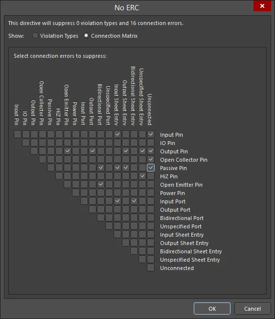
No ERC ダイアログに、Violation Types モード(1 枚目の画像)と Connection Matrix モード(2 枚目の画像)が表示されている例
このダイアログには、上記の No ERC モードの Properties パネルの Suppressed Violations 領域にある Specific Violations をクリックしてアクセスします。

Options and Controls of the No ERC ダイアログ
-
Top statement - このステートメントにより、現在いくつの違反タイプおよび接続エラーが抑制されているかを素早く確認できます。ダイアログ内で変更を行うと、このステートメントは更新されます。
-
Show - Violation Types または Connection Matrix のいずれかを選択して、それぞれの No ERC 指示子を表示および設定します。
Violation Types
このモードでは、違反タイプを抑制または抑制解除できます。
-
Violation Type To Suppress - 設定可能な違反タイプの一覧を表示します。
-
Report Mode - 一覧に表示されている違反タイプの現在のレポートモードを表示します。
-
Suppress - 対応する違反タイプを抑制するにはチェックを入れ、抑制解除するにはチェックを外します。
右クリックメニュー
以下の右クリックメニューコマンド内の [xxx] は、右クリックしたときに選択されていた(またはカーソルがホバーしていた)違反タイプに応じて変化します。
Violations Associated with エントリを右クリックして、そのオブジェクト全体に対する右クリックメニューコマンドにアクセスすることもできます。
-
Suppress only "[xxx]" - 引用符内に列挙されている違反タイプのみを抑制します。
-
Unsuppress only "[xxx]" - 引用符内に列挙されている違反タイプのみを抑制解除します。
-
Suppress All "[xxx]" - 引用符内に列挙されているオブジェクトのすべての違反タイプを抑制します。
-
Unsuppress All "[xxx]" - 引用符内に列挙されているオブジェクトのすべての違反タイプを抑制解除します。
-
Suppress All - オブジェクトやカーソル位置に関係なく、一覧に表示されているすべての違反タイプを抑制します。
-
Unsuppress All - オブジェクトやカーソル位置に関係なく、一覧に表示されているすべての違反タイプを抑制解除します。
-
Toggle All - すべての違反タイプの Suppress チェックボックスをトグルします。
Connection Matrix
このモードでは、接続エラーを抑制または抑制解除できます。
-
Grid - グリッド内のチェックボックスを使用して、目的の接続エラーを抑制(チェックあり)または抑制解除(チェックなし)します。
チェックボックスにカーソルをホバーすると、そのチェックボックスと対応する接続が太字で強調表示されるため、目的の接続エラーを更新しやすくなります。
右クリックメニュー
以下の右クリックメニューコマンド内の [xxx] は、右クリックしたときに選択されていた(またはカーソルがホバーしていた)接続エラーに応じて変化します。
-
Suppress only "[xxx]" - 引用符内に列挙されている接続エラーのみを抑制します。
-
Unsuppress only "[xxx]" - 引用符内に列挙されている接続エラーのみを抑制解除します。
-
Suppress All "[xxx]" - 引用符内にあるすべての接続エラーを抑制します。接続の各側に対して 2 つのコマンドがあります。
-
Unsuppress All "[xxx]" - 引用符内にあるすべての接続エラーを抑制解除します。接続の各側に対して 2 つのコマンドがあります。
-
Suppress All - グリッド内のすべての接続エラーを抑制します。
-
Unsuppress All - グリッド内のすべての接続エラーを抑制解除します。
-
Toggle All - すべての接続エラーのチェックボックスをトグルします。チェックありはチェックなしに、チェックなしはチェックありに切り替わります。
Specific No ERC 指示子は、複数のエラー/警告を生成する回路をサポートするために、複数の違反を対象とするように設定できます。
-
SCH List および SCH Filter パネルから編集します。List パネルを使用すると、1 つ以上のドキュメントから設計オブジェクトを表形式で表示でき、オブジェクト属性の迅速な確認と変更が可能になります。適切なフィルタリング(該当する Filter パネルや Find Similar Objects ダイアログ を使用)と組み合わせることで、アクティブフィルタの範囲に含まれるオブジェクトだけを表示でき、複数の設計オブジェクトをより正確かつ効率的にターゲットして編集できます。

汎用の No ERC 指示子は、Properties パネル(Suppressed Violations セクション内)から、あるいは SCH List パネル上の Suppress Specific Violations プロパティをトグルすることで、素早く Specific No ERC 指示子に切り替えることができ、その逆も可能です。
No ERC 指示子の無効化
No ERC 指示子を削除する代わりに、非アクティブ(バリデーション上は無効)にすることができます。この状態は、指示子の Active プロパティを切り替えることで変更できます。これは、いずれの編集方法からでも利用可能です。非アクティブな No ERC 指示子は、デザイン空間上でグレー表示されます。

No ERC 指示子の使用を一時的にやめたい場合は、削除するのではなく非アクティブにしてください。
No ERC 指示子の印刷制御
既定では、No ERC マーカーは印刷時に含まれます。これを制御して、完全に印刷対象から外すか、特定のシンボルだけを除外するには、以下に示すように Print ダイアログ を使用します。

Print ダイアログで No ERC マーカーの印刷を制御します。
No ERC
 No ERC マーカーを使用して、回路内の特定ノードに対するエラー/警告メッセージを抑制します。
概要
No ERC オブジェクトは設計指示子です。これは回路内のノード上に配置され、回路図プロジェクトのコンパイル時に検出される、すべての Electrical Rule Check の警告および/またはエラー違反状態を抑制します。No ERC を使用して、警告が発生することが分かっている回路上の特定ポイント(未接続ピンなど)で意図的にエラーチェックを制限しつつ、回路の残りの部分については包括的なチェックを実行します。
No ERC 指示子は複数のスタイルをサポートしており、任意の色で表示できます。この機能を利用して、その回路ポイントに対する設計意図を反映させてください。
そのポイントでの機能を最もよく表す No ERC スタイルを選択してください。
No ERC 指示子には 2 種類あります:
-
All Violations – あり得るすべての警告および/またはエラー状態を抑制します。
-
Specific Violations – 選択した警告またはエラー状態のみを抑制し、それ以外の警告やエラーは検出・報告されます。
利用可能性
No ERC 設計指示子は、回路図エディタでのみ配置可能です。No ERC 指示子を配置するには:
-
メインメニューから Place » Directives » Generic No ERC をクリックして、すべての違反を対象とするよう事前設定された No ERC マーカーを配置します。これは汎用 No ERC 指示子(Generic No ERC directive)と呼ばれることがあります。
-
回路図エディタ内で右クリックし、Place » Directives » Generic No ERC をクリックします。
配置 - 汎用 No ERC 指示子
コマンドを起動すると、カーソルは十字カーソルに変わり、配置モードに入ります。No ERC 指示子を配置するには、次の操作を行います:
-
カーソルをワイヤまたは他のネットオブジェクト上に移動し、その回路ポイントに指示子を配置するために Enter をクリックします。
-
続けて他の No ERC 指示子を配置するか、右クリックするか Esc を押して配置モードを終了します。
配置中に実行できる追加操作は次のとおりです:
配置中に属性を変更することは可能ですが(Tab を押して Properties パネルにアクセス)、これらは Permanent オプションが Preferences ダイアログのSchematic – Defaults ページで有効になっていない限り、以降の配置に対する既定設定になります。このオプションを有効にすると、変更は配置中のオブジェクトと、同一配置セッション中に配置される後続オブジェクトにのみ適用されます。
グラフィカル編集
No ERC マーカーは、その位置を変更する以外にグラフィカルに修正することはできません。No ERC マーカーを移動するには、クリックして押したままドラッグし、新しい位置に移動します。
Locked プロパティが有効なオブジェクトをグラフィカルに修正しようとすると、編集を続行するかどうかを確認するダイアログが表示されます。Protect Locked Objects オプションが Preferences ダイアログのSchematic – Graphical Editing ページで有効になっており、かつその設計オブジェクトに対して Locked オプションも有効な場合、そのオブジェクトは選択もグラフィカル編集もできません。ロックされたオブジェクトをクリックして選択し、Locked プロパティを List パネルで無効にするか、Protect Locked Objects オプションを無効にして、そのオブジェクトをグラフィカルに編集できるようにします。
非グラフィカル編集
非グラフィカル編集には、次の方法が利用できます。
No ERC ダイアログまたはプロパティパネルによる編集
パネル ページ: No ERC Properties
この編集方法では、関連する No ERC ダイアログと Properties パネルモードを使用して、オブジェクトのプロパティを変更します。

 No ERC ダイアログ(1 枚目の画像)と Properties パネルの No ERC モード(2 枚目の画像)
配置後、No ERC ダイアログには次の方法でアクセスできます:
-
配置済みの No ERC オブジェクトをダブルクリックします。
-
No ERC オブジェクト上にカーソルを置き、右クリックしてコンテキストメニューから Properties を選択します。
配置中は、Properties パネルの No ERC モードに Tab キーを押してアクセスできます。No ERC を配置すると、すべてのオプションが表示されます。
配置後、Properties パネルの No ERC モードには、次のいずれかの方法でアクセスできます:
-
Properties パネルがすでにアクティブな場合は、No ERC オブジェクトを選択します。
-
No ERC オブジェクトを選択した後、ワークスペース右下の Properties パネルを パネルs ボタンから選択するか、メインメニューから View » パネルs » Properties を選択します。
Double Click Runs Interactive Properties オプションがPreferences ダイアログの Schematic - Graphical Editing ページで無効(既定)になっている場合、プリミティブをダブルクリックするか、選択したプリミティブを右クリックして Properties を選択すると、ダイアログが開きます。Double Click Runs Interactive Properties オプションが有効な場合は、Properties パネルが開きます。
ダイアログとパネルでオプションは同じですが、オプションの順序や配置は若干異なる場合があります。
関連プロパティダイアログによる編集
この編集方法では、No ERC ダイアログを使用して、特定 No ERC オブジェクトの違反タイプおよび接続エラーを変更します。
と Connection Matrix モード(2 枚目の画像)")
 No Erc ダイアログの Violation Types モード(1 枚目の画像)と Connection Matrix モード(2 枚目の画像)
このダイアログには、Specific Violations をクリックしてアクセスします。クリック場所は Suppressed Violations 領域の No ERC ダイアログ、または Properties パネルの No ERC モードです。
特定 No ERC 指示子は、複数のエラー/警告を生成する回路をサポートするために、複数の違反を対象とするよう構成できます。
複数オブジェクトの編集
Properties パネルは複数オブジェクト編集をサポートしており、現在選択されているすべてのオブジェクトで同一のプロパティ設定をまとめて変更できます。同一タイプのオブジェクトを手動で複数選択するか、Find Similar Objects ダイアログ 、または SCH Filter や SCH List パネルを使用して選択した場合、Properties パネル内でアスタリスク(*)が表示されていないフィールドは、選択されたすべてのオブジェクトに対して編集できます。

リストパネルによる編集
パネル ページs: SCH List, SCH Filter
List パネルを使用すると、1 つ以上のドキュメントから設計オブジェクトを表形式で表示でき、オブジェクト属性の迅速な確認と変更が可能になります。適切なフィルタリング(該当する Filter パネル、または Find Similar Objects ダイアログ を使用)と組み合わせることで、アクティブフィルタの範囲に含まれるオブジェクトのみを表示し、対象オブジェクトを絞り込んで、より正確かつ効率的に複数の設計オブジェクトを編集できます。
No ERC Properties
回路図エディタのオブジェクトプロパティは、配置されたオブジェクトの表示スタイル、内容、動作を指定する定義可能なオプションです。各オブジェクトタイプのプロパティ設定は、次の 2 通りの方法で定義されます:

-
Post-placement settings – すべての No ERC オブジェクトプロパティは、デザイン空間内で配置済みの No ERC を選択したときに、No ERC ダイアログおよび Properties パネルで編集可能です。

Double Click Runs Interactive Properties オプションが
Preferences ダイアログの
Schematic - Graphical Editing ページ で無効(デフォルト)になっている場合、プリミティブをダブルクリックするか、選択したプリミティブを右クリックして
Properties を選択すると、ダイアログが開きます。
Double Click Runs Interactive Properties オプションが有効な場合は、
Properties p
anel が開きます。
ダイアログとパネルでオプション自体は同じですが、オプションの順序や配置は若干異なる場合があります。
以下のプロパティ一覧では、Preferences ダイアログ ではデフォルト設定として使用できないオプションには「Properties panel only」と記載されています。
Location (Properties panel only)
-
(X/Y)
-
X (最初のフィールド) - オブジェクトの基準点の現在の X(水平)座標で、現在のデザイン空間の原点を基準とします。編集してオブジェクトの X 位置を変更します。値はメートル法またはヤード・ポンド法のいずれでも入力できます。現在のデフォルト単位以外の単位で値を入力する場合は、単位を含めて入力してください。
-
Y (2 番目のフィールド) - オブジェクトの基準点の現在の Y(垂直)座標で、現在の原点を基準とします。編集してオブジェクトの Y 位置を変更します。値はメートル法またはヤード・ポンド法のいずれでも入力できます。現在のデフォルト単位以外の単位で値を入力する場合は、単位を含めて入力してください。
-
Rotation - ドロップダウンを使用して回転を選択します。
Properties
-
Color - カラーボックスをクリックしてドロップダウンを開き、デフォルト色を選択します。
-
Symbol - ドロップダウンを使用して、利用可能な選択肢からデフォルトを選択します。
-
Active - 有効にするとプリミティブがアクティブになります。
Suppressed Violations (Properties panel only)
-
All Violations - このオブジェクトに対するすべての違反を表示する場合に選択します。違反の Violation Type および Report Mode がグリッドに表示されます。
-
Specific Violations - このオブジェクトに対する特定の違反のみを表示する場合に選択します。違反の Violation Type および Report Mode がグリッドに表示されます。
-
Add - クリックして No ERC ダイアログを開き、新しい違反を追加します。OK をクリックすると、新しい違反がグリッドに追加されます。現在選択されている違反を削除するには、
 をクリックします。
PCB Design Violation Types
バスに関連する違反
Bus indices out of range
この違反は、バスに接続されている構成ネットのインデックスが、そのバスが関連付けられているネットで指定された範囲外にある場合に発生します。
Messages パネルでの通知
通知は Messages パネルに次の形式で表示されます。
Bus index out of range on <NetPrefix> Index = <NetIndex>
ここで、
-
NetPrefix は、バスに接続されている構成ネットのプレフィックスです(例: バスがネット A[0..7] に関連付けられている場合、ネット A8 に対する A など)。.
-
NetIndex は構成ネットの誤ったインデックスです(例: ネット A8 のインデックスが 8 である場合)。
解決のための推奨事項
問題のネットのインデックスを修正して正しい範囲内に収まるようにするか、ネット名自体を変更してください。後者は、そのネットを誤って命名しており、バスオブジェクトによって伝送されるネットの構成要素ではない場合に典型的です。
Bus range syntax errors
この違反は、バスが関連付けられているネットの構文が正しく指定されていない場合に発生します。
Messages パネルでの通知
通知は Messages パネルに次の形式で表示されます。
Bus range syntax error <NetName> at <Location>
ここで、
-
NetName は、問題のバスオブジェクトが関連付けられている親ネットの名前です。
-
Location は、問題のバスオブジェクトの電気的ホットスポットの X, Y 座標です。
解決のための推奨事項
問題のネット識別子(ネットラベル、ポート、シートエントリなど)のバス構文を正しく定義してください。正しい構文は次のいずれかの形式になります。
-
NetName[LowerIndex..UpperIndex]
-
NetName[UpperIndex..LowerIndex]
たとえば、2 つの構成ネット A0 と A1 を運ぶバスを考えます。この場合のバス構文は A[0..1] または A[1..0] である必要があります。不正な構文の例としては、A[0.1]、A[1-0]、A[0,1]、A[..1]、A[0..] などがあります。
Illegal bus range values
この違反は、バスに関連付けられたネットの構文内に、少なくとも 1 つのインデックスが負の値として指定されている場合に発生します。
Messages パネルでの通知
通知は Messages パネルに次の形式で表示されます。
Illegal bus range value <BusLabel> at <Location>
ここで、
-
BusLabel は、不正な値が検出されたバスラベリングの定義です。
-
Location は、問題のバスオブジェクトの電気的ホットスポットの X, Y 座標です。
解決のための推奨事項
問題のネット識別子(ネットラベル、ポート、シートエントリなど)のバス構文を正しく定義してください。正しい構文は次のいずれかの形式になります。
-
<NetName>[<LowerIndex>..<UpperIndex>]
-
<NetName>[<UpperIndex>..<LowerIndex>]
LowerIndex および UpperIndex は 0 または正の整数である必要があり、負の値にすることはできません。
Mismatched bus label ordering
この違反は、同じバススライスに関連付けられた 2 つのネット識別子が、バスラベルの順序を同じ方向(昇順または降順)で定義していない場合に発生します。
Messages パネルでの通知
通知は Messages パネルに次の形式で表示されます。
Mismatched bus ordering on <NetName> Low value first and High value first
ここで、
-
NetName は、順序が不一致なバスが関連付けられている親ネットの名前です。
解決のための推奨事項
バスの順序が一貫していないネット識別子(ポート、ネットラベル、シートエントリなど)を特定します。正しい順序を決定し、誤っているオブジェクトの名前を修正してください。
Mismatched bus widths
この違反は、同じバススライスに関連付けられた 2 つのネット識別子が、異なる幅のバスラベルを定義している場合に発生します。たとえば、名前が A[0..7] のポートが、接続先のバスに対して A[0..15] と定義されたネットラベルを持っている場合などです。
Messages パネルでの通知
通知は Messages パネルに次の形式で表示されます。
Mismatched bus widths on bus section <NetName> (<BusSize1> and <BusSize2>)
ここで、
-
NetName は、幅が不一致なバスオブジェクトが関連付けられている親ネットの名前です。
-
BusSize1 は、問題のバスオブジェクトのうち 1 つ目の幅です。
-
BusSize2 は、問題のバスオブジェクトのうち 2 つ目の幅です。
解決のための推奨事項
バスラベルの幅が一貫していないネット識別子(ポート、ネットラベル、シートエントリなど)を特定します。正しい幅を決定し、誤っているオブジェクトの名前を修正してください。
Mismatched Bus/Wire object on Wire/Bus
この違反は、ワイヤオブジェクトが誤ってバスに接続されている場合、またはバスオブジェクトが誤ってワイヤに接続されている場合に発生します。たとえば、ポート A がバスに接続されているにもかかわらず、そのポート名に正しいバスラベル構文(例: A[0..1])が入力されていない場合です。実質的には、そのポートは単一信号(ワイヤ)オブジェクトでありながら、誤ってバスに接続されていることになります。
Messages パネルでの通知
通知は Messages パネルに次の形式で表示されます。
<ObjectIdentifier> at <Location> placed on a <ObjectType>
ここで、
-
ObjectIdentifier は不一致オブジェクトを表し、バスまたはワイヤオブジェクト(ピン、ポート、パワーポート、ネットラベル、オフシートコネクタ、シートエントリなど)のいずれかになります。識別子は次の 2 つの形式のいずれかで表示されます。
-
バスの場合 –
Bus <Object> <Name>(例: Bus Net Label GND_BUS[..])。
-
ワイヤの場合 –
Wire <Object> <Name>(例: Wire Port TXD)。
-
Location は、そのオブジェクトの電気的ホットスポットの X,Y 座標です。
-
ObjectType は、問題のオブジェクトが配置されている対象であり、ワイヤまたはバスのいずれかです。
解決のための推奨事項
問題を解決するには、次の点を検討してください。
-
Is the connection correct? – オブジェクトに接続されているバスは、本来ワイヤであるべきではないか、その逆ではないかを確認します。
-
Is the object defined correctly? – バスオブジェクトの場合、オブジェクト名が
<Name>[<LowIndex>..<HighIndex>] または <Name>[<HighIndex>..<LowIndex>] の形式で正しいバス構文を使用して指定されていることを確認します。たとえば、1 バイト幅のデータ出力ポートは DAT_OUT[7..0] のように指定できます。ワイヤオブジェクトの場合、オブジェクト名が単一信号を定義しており、バス構文で定義されていないことを確認します。
Mixed generic and numeric bus labeling
この違反は、同じバススライスに接続されている 2 つのネット識別子(ポート、ネットラベル、シートエントリなど)が、異なるバス構文を使用している場合に発生します。1 つは数値形式(例: A[0..2])でバス範囲を定義し、もう 1 つはジェネリック形式(例: A[0..b])で範囲を定義している場合です。
Messages パネルでの通知
通知は Messages パネルに次の形式で表示されます。
Mismatched generic and numeric bus labeling on <NetName> <Level> value first and Generic
ここで、
-
NetName は、ラベリングが不一致なバスが関連付けられている親ネットの名前です。
-
Level は、ネットの数値順序に依存します。昇順(例: [0..2])の場合、Level は Low と表示されます。降順(例: [2..0])の場合、Level は High と表示されます。
解決のための推奨事項
バスラベル指定が誤っているオブジェクトを特定し、そのラベル指定を正しく修正してください。
バス名での Generics の使用はサポートされていません。必ず数値を使用してください。
コンポーネントに関連する違反
Component has been deleted
この違反は、プロジェクト設計から少なくとも 1 つのコンポーネントが削除されたときに発生します。「ソフト削除」として動作し、削除されたコンポーネントは専用の Trash 場所に移動され、Restore で復元するか、Permanently Delete で完全に削除することができます。これらの操作は、接続された Workspace のブラウザーインターフェース内で、削除済みエントリのメニューオプション (⋯) から実行します。
メッセージパネルでの通知
Messages パネルに、次の形式で通知が表示されます:
ComponentName: Component has been deleted
ここで:
-
ComponentName は Workspace コンポーネントの名前です。
解決のための推奨事項
コンポーネントを誤って削除した場合は、適切なアクセス権を持つユーザーが Workspace のブラウザーインターフェースの Trash ページから復元できます。そうでない場合は、設計で使用しているコンポーネントを、接続された Workspace で is 利用可能な同等コンポーネントに置き換えてください。
Component Implementations with invalid pin mappings
この違反は、Integrated Library Package (*.LibPkg) をコンパイルした際に、回路図コンポーネントとリンクされたモデル間のピンマッピングが無効であることが判明した場合に発生します。
メッセージパネルでの通知
Messages パネルに、次の形式で通知が表示されます:
ComponentName: Could not find port <ModelPinNumber> on model <ModelName> for pin <ComponentPinNumber> – PCB モデル関連
ComponentName: Could not map port <ModelPinNumber> on model <ModelName> to a pin – シミュレーションモデル関連
ここで:
-
ComponentName はソース回路図ライブラリ内のコンポーネント名です。
-
ModelPinNumber は、リンクされたモデル上で見つからなかったピン/パッドに対して期待されるデジグネータです。
-
ModelName はコンポーネントにリンクされているモデル名です。
-
ComponentPinNumber は、モデルの誤ったピンがマッピングされている、ソース回路図コンポーネント上のピンのデジグネータです。
解決のための推奨事項
解決には、回路図シンボルとターゲットドメインモデル間のマッピングにアクセスする必要があります。そのためには、まず対象となる回路図ライブラリコンポーネントのプロパティを表示する必要があります。SCH Library パネル の Components リストでコンポーネントのエントリをダブルクリックし、そのコンポーネントのプロパティが読み込まれた Properties パネル にアクセスします。
PCB モデル関連の違反メッセージが表示されている場合は、パネルの Footprint セクションでモデルを選択し、リスト下の  ボタンをクリックして PCB Model ダイアログ にアクセスします。そこで Pin Map ボタンをクリックして Model Map ダイアログ を開きます。Component Pin Designator 列で、メッセージでフラグが立てられているピン番号 (
ComponentPinNumber) を探します。違反は、対応する Model Pin Designator 列のエントリが、PCB モデル内に存在しないパッドデジグネータを指しているために発生します。必要に応じてエントリを修正してください。通常は 1 対 1 のマッピングとなり、両側のデジグネータは同じになります。
シミュレーションモデル関連のメッセージが表示されている場合は、パネルの Models セクションでモデルを選択し、リスト下の ボタンをクリックして Sim Model ダイアログにアクセスします。そこで Port Map タブをクリックします。モデルピンが回路図コンポーネントのピンに正しくマッピングされていない場合に、この違反が発生します。これは、モデルピンのエントリがすでにマッピングされているピン、または Not Connected に設定されている場合に起こり得ます。必要に応じてエントリを修正してください。
Component revision has inapplicable state
この違反は、接続された Workspace から配置された Component Item Revision の配置インスタンスのうち、少なくとも 1 つが不適用状態であると検出された場合に発生します。たとえば、コンポーネントが現在 Depracated または Obsolete であり、そのため最新の設計スピンには使用すべきでない場合です。適用可否は、State Properties ダイアログ 内の Allowed to be used in designs オプションによって決定されます。Edit Lifecycle Definitions ダイアログ 内から、対象状態のエントリをライフサイクル定義内でダブルクリックするか、そのエントリを選択して表示される編集アイコン ( ) をクリックすることで、このダイアログにアクセスします。このオプションが有効な場合、その状態にある Item Revision は設計で使用することが許可され、「Applicable」と見なされます。このオプションが無効な場合、その状態にある Item Revision は有効に使用することができず、「Inapplicable」(または非適用)と見なされます。
Edit Lifecycle Definitions ダイアログ自体は、
Preferences ダイアログの
Data Management – Servers ページ からアクセスします。アクティブにサインインしている Workspace の
Properties ボタンをクリックし、ドロップダウンメニューから
Lifecycles を選択します。
メッセージパネルでの通知
Messages パネルに、次の形式で通知が表示されます:
Component <Designator> <Comment>: Component revision has inapplicable state
ここで:
-
Designator はコンポーネントインスタンスの Designator です。
-
Comment はコンポーネントインスタンスの Comment です。
解決のための推奨事項
Item Manager ダイアログ を使用して、設計で有効に使用できる Component Item Revision を選択し、置き換えてください。不適用状態にある各コンポーネントについてこれを行います。あるいは、個々のコンポーネントレベルで、既存の Component Item Revision を別のリビジョン、または別の Component Item のリビジョンに切り替えることもできます。回路図上でコンポーネントを選択し、Properties パネル からそのプロパティにアクセスします。パネルの Properties セクションで、Update ボタンをクリックして現在の Component Item の最新リビジョンを使用するか、Design Item ID フィールド右側の  ボタンをクリックして Workspace にアクセスし、使用する別の Component Item Revision を参照して選択します。
Properties パネルまたは Item Manager ダイアログで利用可能なコントロールを使用して、適用可能な状態で is している Item の後続リビジョンを選択するか(これが不可能な場合、つまりその Item 自体が設計用途に適さない場合)、別の Item の適用可能なリビジョンを選択してください。
注意
-
配置済みコンポーネントがソース Workspace との接続を失った場合(たとえば、配置元の Workspace が切断された、または Workspace からサインアウトした場合など)、そのコンポーネントは Component revision has inapplicable state チェックに違反します。これは Messages パネル に、次の形式のエントリとして反映されます: Component <Designator> <Comment>: Can't perform revision status validation: Failed to get session: Access denied! User login required for this service.
-
また、設計リリースプロセス中に、設計内で不正に使用されているコンポーネントを検出することもできます。全体的なリリース検証手順に Component State Checking を追加・設定してください。
Component revision is Out of Date
この違反は、接続された Workspace から配置されたコンポーネントが、最新版ではないと検出された場合に発生します。
メッセージパネルでの通知
Messages パネルに、次の形式で通知が表示されます:
Component <Designator> at <Location>: Component revision is Out of Date
ここで:
-
Designator はコンポーネントインスタンスの Designator です。
-
Location は問題のコンポーネントインスタンスの原点を示す X, Y 座標です。
解決のための推奨事項
Item Manager ダイアログ を使用して、最新リビジョンではないコンポーネントを特定し、更新します。Item Manager には Revision Status 列があり、最新リビジョンではないコンポーネントについては、そのステータスが Out of Date となります。古いコンポーネントを選択し、右クリックしてメニューから Update to latest revision を選択します。これを行った後、影響を受ける回路図にこれらの変更を適用するために Generate an ECO を実行します。
または、個々のコンポーネントレベルで、既存の Component Item Revision を最新リビジョンに切り替えることもできます。回路図上でコンポーネントを選択し、Properties パネル からそのプロパティにアクセスします。パネルの Properties セクションで、Update ボタンをクリックして、現在の Component Item の最新リビジョンを使用します。
注意
配置済みコンポーネントがソース Workspace との接続を失った場合(たとえば、配置元の Workspace が切断された、または Workspace からサインアウトした場合など)、そのコンポーネントは Component revision is Out of Date チェックに違反します。これは Messages パネルに、次の形式のエントリとして反映されます: Component <Designator> <Comment>: Can't perform revision status validation: Failed to get session: Access denied! User login required for this service.
Components containing duplicate sub-parts
この違反は、マルチパートコンポーネントインスタンスの同じパートが、回路図設計内に 2 回以上配置された場合に発生します。たとえば、デジグネータ U9 の 74HC32 コンポーネントを配置したが、誤ってこのコンポーネントのパート 1 を 2 回配置してしまい、設計内に U9A が 2 つ存在するような場合です。
メッセージパネルでの通知
Messages パネルに、次の形式で通知が表示されます:
Component <ComponentName> has duplicate sub-parts at <Location1> and <Location2>
ここで:
-
ComponentName は、デジグネータとライブラリ参照で表される問題のコンポーネント名です。
-
Location1 は、該当サブパートの最初のインスタンスの X, Y 座標です。
-
Location2 は、該当サブパートの重複インスタンスの X, Y 座標です。
解決のための推奨事項
問題のパーツについて、必要に応じてパート番号を変更します。これは Increment Part Number コマンドを使用して行います。このコマンドはメインの Edit メニュー、または(パート上で右クリックしたときの)Part Actions サブメニューから利用できます。Edit メニューからコマンドを起動する利点は、インクリメントモードのままになるため、目的の番号に到達するまでパート番号を順に切り替えられる点です。
Components with duplicate pins
この違反は、コンポーネント内の 2 つ以上のピンが同じデジグネータを持っている場合に発生します。
メッセージパネルでの通知
Messages パネルに、次の形式で通知が表示されます:
Duplicate pins in component Pin <Identifier1> and Pin <Identifier2>
ここで:
-
Identifier1 は、複製されたピンの最初のインスタンスを表す識別子で、部品デザインator-ピンデザインatorの組み合わせで表されます。
-
Identifier2 は、複製されたピンの 2 番目のインスタンスを表す識別子で、部品デザインator-ピンデザインatorの組み合わせで表されます。
解決のための推奨事項
問題となっているピンのデザインatorを変更し、それぞれが一意に割り当てられるようにします。すでに配置済みコンポーネントのピンデザインatorは、回路図エディタ内で編集できます。
通常、この重複はライブラリコンポーネント内に存在するため、その場合はソース回路図ライブラリ内で該当コンポーネントのピンデザインatorを編集し、Update From Libraries(回路図エディタ)または Update Schematics(回路図ライブラリエディタ)コマンドを使用して、変更を配置済みコンポーネントインスタンスに反映させます。これら両コマンドは、それぞれのエディタのメイン Tools メニューから利用できます。
注意
Messages パネルには、各コンポーネントごとに 1 つの違反インスタンスのみがリストされます。コンポーネントに同じデザインatorを持つピンが 2 つ以上存在する場合でも、パネルの Details 領域で違反を調査するときには、最初の 2 つの重複ピン(ピン名のアルファベット順)が表示されるだけです。
Duplicate Part Designators
この違反は、設計内のソース回路図シート間で、少なくとも 2 つの部品が同じデザインatorを持っている場合に発生します。
Messages パネルでの通知
通知は、Messages パネルに次の形式で表示されます。
Duplicate Component Designators <PartDesignator>
ここで:
-
PartDesignator は問題となっているデザインatorです。
解決のための推奨事項
必要に応じて、重複しているデザインatorに対して、互いに異なる一意のデザインatorを割り当てます。これは、各問題のあるデザインatorを手動で編集するか、Annotate ダイアログ(Tools » Annotation » Annotate Schematics)を使用して行うことができます。
あるいは、まず Tools » Annotation » Reset Duplicate Schematic Designators コマンドを使用して重複しているコンポーネントデザインatorをリセットし、その後 Tools » Annotation » Annotate Schematics Quietly コマンドを使用して Annotate ダイアログを起動せずにアノテートを行います。
Generic Component
この違反は、Generic Component が最終設計に含まれている場合に発生します。Generic Components は、利用可能なコンポーネントソースから特定のメーカー部品を探して選択することなく、設計に素早く配置できるもので、後から適切なコンポーネントに容易に置き換えられるプレースホルダとして意図されています。
Messages パネルでの通知
通知は、Messages パネルに次の形式で表示されます。
Generic Component <PartDesignator> is placed at <Location>
ここで:
-
Designator は、配置された Generic Component インスタンスの Designator です。
-
Location は、問題となっている Generic Component インスタンスの原点を示す X, Y 座標です。
解決のための推奨事項
設計が進み、Generic Component を特定の物理コンポーネントに置き換えられる段階になったら、Properties パネルの Design Item ID field で三点リーダーメニューを選択し、Replace Component ダイアログ を使用できます。これは Item Manager から、またはプロジェクトの ActiveBOM document を通じても実行できます。
Mismatched hidden pin connections
この違反は、マルチパートコンポーネントにおいて、複数のサブパートで共通の非表示ピンが異なるネットに接続されている場合に発生します。
Messages パネルでの通知
通知は、Messages パネルに次の形式で表示されます。
Mismatched hidden pin connections in Pin <Identifier> and Pin <Identifier>
ここで:
-
Identifier は、問題となっているピンを識別するために使用されます。この識別子は PhysicalComponentName-PinDesignator(例: U2-7)という形式で表示されます。
解決のための推奨事項
問題となっているピンを正しいネットに再割り当てします。非表示ピンは、対応する List パネル(SCHLIB List パネルまたは SCH List パネル)がピンプロパティを表示しているときに、その Hidden Net Name フィールドにネット名を入力することでネットに割り当てられます。これを SCH List パネルで行う場合は、パネル内で右クリックし、ピンをパネルにリスト表示するために Show Children オプションを有効にします。
Mismatched pin visibility
この違反は、マルチパートコンポーネントの電源ピン(VCC および GND)に関連しています。通常、これらのピンはパート 0 に関連付けられ、設計の VCC および GND ネットに自動的に接続され、非表示になっています。コンポーネントパートのいずれかでこのようなピンの可視性を有効にすると、そのピンはもはや対象の電源ネットに接続されなくなり、エラーがフラグされます。
Messages パネルでの通知
通知は、Messages パネルに次の形式で表示されます。
Pin is visible in one sub-part and hidden in another sub-part
解決のための推奨事項
設計空間で問題となっている電源ピンの表示を無効にするか、ピンを表示したままにする場合は、そのピンに VCC および/または GND の電源ポートオブジェクトが適切に接続されていることを確認します。
Missing Component Models
この違反は、Integrated Library Package(*.LibPkg)をコンパイルする際に、ソース回路図ライブラリ内のコンポーネントにリンクされているモデルが見つからなかった場合に発生します。
Messages パネルでの通知
リンクされているモデルがフットプリントモデルまたはシミュレーションモデルである場合、通知は Messages パネルに次のいずれかの形式で表示されます。
<ComponentName>: Could not find <ModelName> – モデル検索スコープが Any の場合。
<ComponentName>: Could not find <ModelName> in <LibraryName> – モデル検索スコープが Library Name の場合。
<ComponentName>: Could not find <ModelName> in <Path> – モデル検索スコープが Library Path の場合。
ここで:
-
ComponentName は、ソース回路図ライブラリ内のコンポーネント名です。
-
ModelName は、ソースコンポーネントにリンクされており、見つからなかったフットプリントまたはシミュレーションモデルの名前です。
-
LibraryName は、リンクされたモデルを含むと指定されているライブラリファイルの名前です。
-
Path は、リンクされたモデルを含むと指定されているライブラリファイルへの絶対パスです。
リンクされているモデルがシグナルインテグリティモデルである場合、メッセージは Messages パネルに次の形式で表示されます。
<ComponentName>: Could not find 'GenericEntity' in <Path>
ここで:
-
ComponentName は、ソース回路図ライブラリ内のコンポーネント名です。
-
Path は、ライブラリ/モデルへの絶対パスです。
解決のための推奨事項
リンクされたフットプリントまたはシミュレーションモデルが原因の場合
この問題は、通常次のいずれかの状況によって引き起こされます。
-
モデルリンクを定義する際に、モデル名が誤って指定されている。
-
リンクされたモデルが、指定されたライブラリファイル内に存在しない。
-
リンクされたモデルを含むライブラリファイルが移動または削除されている。
この違反を解決するための最初の確認先は、リンク先のモデルタイプに対応するセットアップダイアログ、すなわち PCB Model ダイアログ または Sim Model ダイアログです。いずれの場合も、次の点を確認します。
-
リンク先モデルの名前が正しいこと。
-
そのモデルが存在するライブラリ/モデルファイルを特定するために、正しいオプションが使用されていること。
表示されるエラーメッセージの形式は、モデルを検索する際に有効にしている検索スコープによって異なり、モデルリンクの問題を追跡するうえで大いに役立ちます。
-
指定パス内でモデルが見つからない場合(検索スコープ:
Library path)、指定したライブラリ/モデルファイルがその場所に実際に存在することを確認し、さらにそのライブラリ/モデルファイル内に指定名のモデルが存在するかを確認します。
-
指定されたライブラリ/モデルファイル内でモデルが見つからない場合(検索スコープ:
Library name)、そのライブラリ/モデルファイルが Available Libraries リスト(Project Libraries、Installed Libraries、Project Search Paths)に追加されていることを確認します。また、そのライブラリ/モデルファイルに、リンクで指定した名前と同じモデルが含まれていることも確認します。
-
モデルが単に見つからない場合(検索スコープ:
Any)、リンクで指定した名前と同じモデルを含むライブラリ/モデルファイルが Available Libraries リストに追加されていることを確認します。
リンクされたシグナルインテグリティモデルが原因の場合
通常、シグナルインテグリティモデルの種類(例:ダイオード、IC)が指定されていない場合に発生します。これは、シグナルインテグリティモデル用の関連する設定ダイアログで解決できます。最も簡単なアクセス方法は、選択したコンポーネントのプロパティを表示しているときに、Properties パネル を使用することです。パネルの General タブの Models セクションで正しいモデルを使用しているか確認し、必要に応じて修正してください。Add および ボタンを使用して新しいモデルを作成(リストから Signal Integrity を選択)するか、既存のシグナルインテグリティモデルを修正できます。これにより Signal Integrity Model ダイアログにアクセスでき、Import Ibis ボタンを使用して Ibis モデルファイルからピンモデルをインポートできます。
Ibis モデルは、Add » Ibis model をクリックして直接追加することもできます。その後に表示される Ibis Model ダイアログを使用して、モデルおよびファイルへのリンクを定義します。
Missing pin found in component display mode
この違反は、部品のいずれかの表示モードでピンの欠落が検出された場合に発生します。
メッセージパネルでの通知
Messages パネルには、次の形式で通知が表示されます。
<NumberOfMissingPins> missing pins in <DisplayMode> of design item <DesignItemID>
ここで:
-
NumberOfMissingPins は、その部品で見つかった欠落ピンの数です。
-
DisplayMode は、欠落ピンが見つかった、その部品の特定のグラフィカル表現モードです。部品には Normal モードがあり、最大 255 個までの Alternate モードを定義できます。
-
DesignItemID は、問題の部品の Design Item ID プロパティです。
解決のための推奨事項
この違反は通常、コンポーネントに代替グラフィカルモードが定義されているものの、Normal モードで指定されているすべてのピンが Alternate モードで指定されていない場合に発生します(つまり、グラフィカル表示モード間でピン数が同一でなければなりません)。
元の回路図ライブラリで、既存の表示モードから不足しているピンをコピーし、そのコンポーネントの問題の表示モードに貼り付けます。これは、すでに配置済みの部品に対して回路図シート上で直接行うこともできますが、通常はライブラリ内で問題に対処し、その後変更を反映させます(Tools » Update Schematics)。
Sheet Symbol with duplicate entries
この違反は、シートシンボル内に同じ名前を持つ 2 つのシートエントリが存在する場合に発生します。
メッセージパネルでの通知
Messages パネルには、次の形式で通知が表示されます。
Sheet Symbol with duplicate entries Sheet Entry <Identifier> at <Location1> and <Location2>
ここで:
-
Identifier は、問題のシートエントリを表すために使用されます。この識別子は SheetSymbolName-SheetEntryName(SheetEntryIOType) という形式で表示されます。
-
Location1 は、1 つ目の違反シートエントリの X, Y 座標です。
-
Location2 は、2 つ目の違反シートエントリの X, Y 座標です。
解決のための推奨事項
必要に応じて、問題のシートエントリオブジェクトの名前を変更します。これは、その場で名前を編集するか、問題のシートエントリをダブルクリックして Properties パネル の Properties セクションでその Name を編集することで行えます。このパネルには、選択したシートエントリのすべてのプロパティが表示されます。
シートエントリ名は、親シートシンボルのプロパティを参照しているときに、
Properties パネル の
General タブ上の
Sheet Entries セクションから編集することもできます。
Sheet Symbols with duplicated indexes
この違反は、multi-channel design において、同じ子回路図シートを参照し、かつ Designator フィールドに Repeat キーワードを含む 2 つ以上のシートシンボルが、同じチャネルインデックス範囲の値を共有している場合に発生します。
メッセージパネルでの通知
Messages パネルには、次の形式で通知が表示されます。
Sheet Symbols <ChannelIdentifier> have duplicated indexes: <ChannelIndexList>
ここで:
-
ChannelIdentifier は、シートシンボルの Designator フィールドで使用されているチャネル識別子です。
-
ChannelIndexList は、問題のシートシンボル間で重複しているチャネルインデックスのカンマ区切りリストです。
解決のための推奨事項
問題のシートシンボルオブジェクトのデジグネータを変更し、それぞれのインデックス範囲が共通の値を持たないようにします。これは、その場でデジグネータを編集するか、問題のシートシンボルをダブルクリックして Properties パネル の Properties セクションでその Designator を編集することで行えます。このパネルには、選択したシートシンボルのすべてのプロパティが表示されます。
Un-Designated parts requiring annotation
この違反は、設計内のコンポーネントにデフォルトデジグネータ(末尾に ? が付く)が付いている場合、すなわちまだアノテートされていないか、デジグネータがリセットされている場合に発生します。
メッセージパネルでの通知
Messages パネルには、次の形式で通知が表示されます。
Un-Designated Part <PartDesignator>
ここで
-
PartDesignator は、未指定部品のデフォルトデジグネータです(例:U?、D?、C? など)。
解決のための推奨事項
必要に応じて、問題のコンポーネントに一意のデジグネータを割り当てます。これは、デジグネータを手動で編集するか、Annotate ダイアログ(Tools » Annotation » Annotate Schematics)を使用して行うことができます。
あるいは、Tools » Annotation » Annotate Schematics Quietly コマンドを使用して Annotate ダイアログを起動せずにアノテートすることもできます。
注意
Messages パネルには、各デジグネータタイプ(U?、D?、C? など)ごとに 1 つのエラーインスタンスのみがリストされます。複数のエラーが存在する可能性があります。
Unused sub-part in component
この違反は、マルチパートコンポーネントインスタンスの一部が設計内で使用されていない場合に発生します。たとえば、74HC32 コンポーネントの 4 パートのうち 3 パートが配置および配線されているが、4 つ目が未使用の場合などです。
なお、プリミティブを含まないパートが回路図に配置されていない場合(かつ、シンボルエディタでシンボルを編集しているときに SCH Library パネルに表示されるシンボルパーツの一覧で、プリミティブを持たないパートがプリミティブを持つすべてのパートの下にリストされている場合)、この違反は発生しません。
メッセージパネルでの通知
Messages パネルには、次の形式で通知が表示されます。
Component <Identifier> has unused sub-part(s) (<PartNumber>)
ここで
-
Identifier は親コンポーネントで、Designator Library Reference という形式で表されます(例:U11 74HC32)。
-
PartNumber は、どのパートが未使用であるかを示す整数です(例:1 はパート A、2 はパート B を表す、など)。
解決のための推奨事項
未使用のパートを配置し、その入力を GND に接続します。同じルートデジグネータを確保するには、そのコンポーネントインスタンスの既存パートをコピーし、貼り付け後にパート番号を適切にインクリメントします。
ドキュメントに関連する違反
Ambiguous Device Sheet Path Resolution
この違反は、Sheet Symbol の File Name フィールドで指定されたターゲットデバイスシートが、複数の宣言済みデバイスシートフォルダ内で見つかった場合に発生します。
メッセージパネルでの通知
Messages パネルには、次の形式で通知が表示されます。
Ambiguous Device Sheet Resolution for <DeviceSheetName>
ここで:
-
DeviceSheetName は、親デバイスシートシンボルの File Name フィールドに対する現在のエントリです。File Name フィールド内のエントリとは異なり、メッセージには拡張子(*.SchDoc)も含まれます。
解決のための推奨事項
Messages パネルの Details 領域を使用して、問題のデバイスシートシンボルへクロスプローブします。シンボルをダブルクリックして Properties パネル からそのプロパティにアクセスします。パネルの General タブ上の Source セクションには、現在使用されているデバイスシートインスタンスへのフルパスが表示されます。
使用されるデバイスシートインスタンスは、宣言済みデバイスシートフォルダ全体を検索した際に最初に検出されたものであり、これらのフォルダは Preferences ダイアログの Data Management – Device Sheets ページ で宣言され、上から下の順に検索されることを忘れないでください。現在使用されているデバイスシートが正しいインスタンスであれば、この違反は無視して構いません。そうでない場合は、正しいインスタンスが存在するフォルダを選択し、そのフォルダがリストの先頭に来るまで Move Up ボタンをクリックします。
ただし、これによりこの特定のデバイスシートに関する即時の問題は解決されるかもしれませんが、あいまいさ自体は残る点に注意してください。この問題を完全に解決するには、冗長なデバイスシートを特定し、それらを他の宣言済みデバイスシートフォルダから削除します。
Circular Document Dependency
この違反は、Design メインメニューから Create Sheet Symbol From Sheet コマンドを使用し、すでにプロジェクト内で子として使用されている回路図ドキュメントを Choose Document to Place ダイアログで選択し、かつ選択した回路図ドキュメント同士に Device Sheet リンクが存在する場合に発生します。
メッセージパネルでの通知
Messages パネルには、次の形式で通知が表示されます。
Circular dependency between document <DocumentName1> and document <DocumentName2>
ここで:
-
DocumentName1 および DocumentName2 は、互いに Device Sheet リンクを持つ 2 つのドキュメント名です。
解決のための推奨事項
エラーメッセージにリストされている回路図ドキュメントを確認し、それらの間の Device Sheet リンクを修正します。
Missing child sheet for sheet symbol
この違反は、シートシンボルとターゲット回路図サブドキュメント間のリンクが無効な場合に発生します。これは次のような場合に起こり得ます。
-
シートシンボルが手動で配置されているが、そのシンボルの File Name フィールドにサブレベルドキュメント参照が入力されていない。
-
シンボルの File Name フィールド内のドキュメント参照が誤って入力されており、実在しないドキュメントを参照している。
-
参照されているターゲットドキュメントがプロジェクトから削除された、または削除されている。
メッセージパネルでの通知
Messages パネルには、次の形式で通知が表示されます。
Missing child-sheet in <SymbolFileName> in Symbol <SymbolDesignator>
ここで:
-
SymbolFileName は、親シートシンボルの File Name フィールドに対する現在のエントリです。
-
SymbolDesignator は、親シートシンボルのデジグネータです。
解決のための推奨事項
シートシンボルがデザイン空間内で選択されている状態で、Properties パネル の General タブにある Properties セクション内の、シートシンボルの File Name フィールドのエントリを確認します。標準のシートシンボルの場合、ターゲットドキュメント自体は同じタブ内の Source セクションで指定され、ソースは Local に設定されます。必要なターゲットドキュメントがすでに存在する場合は、そのドキュメント名(拡張子を含む)がフィールドに正しく入力されていることを確認してください。ターゲットドキュメントがプロジェクトから削除されていて、かつそのドキュメントにアクセスできる場合は、プロジェクトに再追加してください。ターゲットドキュメントが存在しない場合は、シンボルを右クリックし、Sheet Symbol Actions サブメニューから Create Sheet From Symbol コマンドを選択します。
注意
このエラーは、Device Sheet Symbol が配置されているにもかかわらず、ターゲットの Device Sheet が見つからない場合にも生成されます。デバイスシートシンボルがデザイン空間内で選択されている状態で、ターゲットドキュメント自体は Properties パネル の General タブにある Source セクションで指定され、デバイスシートシンボルの場合、ソースは Device に設定されます。
Multiple Top-Level Documents
この違反は、階層デザインにおいて、2 つ以上の回路図シートが構造のトップレベルに存在する場合に発生します。
Messages パネルでの通知
Messages パネルには、次の形式で通知が表示されます。
Multiple top level documents: <SheetName> has been used
ここで、
-
SheetName は、現在トップレベルシートとして使用されている回路図ドキュメントの名前です。
解決のための推奨事項
この問題は通常、真のトップシート上のシートシンボルが、意図したサブシートを正しくターゲットしていないことが原因で発生します。この問題を解決するには、まずどの回路図シートが意図したサブシートであるかを特定します。トップレベル回路図上に、その意図したサブシート用のシートシンボルが配置されているか確認します。
-
シートシンボルが存在しない場合は、手動で配置するか、メインメニューの Design » Create Sheet Symbol From Sheet コマンドを使用して作成します。
-
シートシンボルが存在する場合は、それがサブシートを参照していることを確認します。シートシンボルがデザイン空間内で選択されている状態で、Properties パネル の General タブにある Properties セクション内の、シートシンボルの File Name フィールドのエントリを確認します。ターゲットドキュメント自体は同じタブ内の Source セクションで指定され、標準のシートシンボルの場合、ソースは Local に設定されます。
Port not linked to parent sheet symbol
この違反は、子シート上のポートが、親シートシンボル上のシートエントリと一致していない場合に発生します。親シートシンボル内のすべてのシートエントリは、子シート上の対応するポートと同期(マッチ)していなければなりません。
Messages パネルでの通知
Messages パネルには、次の形式で通知が表示されます。
Port <PortName> not matched to Sheet-Entry at <Location>
ここで、
-
PortName は、子シート上のポート名です。
-
Location は、そのポートの電気的ホットスポットの X, Y 座標です。
解決のための推奨事項
この問題は、次のような理由で発生する可能性があります。
-
そのポートに対応するシートエントリが存在しない。
-
そのポートに対応するシートエントリは存在するが、名前が異なる。
-
そのポートに対応するシートエントリは存在するが、I/O Type が異なる。
該当するポート上で Ctrl+Double Click を使用して親シートシンボルへ昇格します。シートシンボルを右クリックし、表示されるメニューから Sheet Symbol Actions » Synchronize Sheet Entries and Ports を選択します。これにより、そのシートシンボル用の Synchronize Ports To Sheet Entries ダイアログ が開きます。
ダイアログを使用して、問題のポートを必要なシートエントリにマッチさせます。シートエントリが存在しない場合は、ダイアログから直接作成できます。シートエントリが存在するが Name や I/O Type が異なる場合は、マッチングの一環として、Name と I/O Type をポート側とシートエントリ側のどちらから採用するかを決定できます。
注意
シートエントリとポートが存在するものの、Name や I/O Type が異なる場合、「シートエントリがポートとマッチしていない」という内容の対応するエラーメッセージが表示されます。シートエントリをポートと同期させることで、両方のエラーが解消されます。
Sheet Entry not linked to child sheet
この違反は、親シートシンボルで参照されている子シート上に、シートエントリとマッチするポートが存在しない場合に発生します。親シートシンボル内のすべてのシートエントリは、子シート上の対応するポートと同期(マッチ)していなければなりません。
Messages パネルでの通知
Messages パネルには、次の形式で通知が表示されます。
Sheet-Entry <SheetEntryName> not matched to Port at <Location>
ここで、
-
SheetEntryName は、親シートシンボルに関連付けられているシートエントリの名前です。
-
Location は、そのシートエントリの電気的ホットスポットの X, Y 座標です。
解決のための推奨事項
この問題は、次のような理由で発生する可能性があります。
-
そのシートエントリに対応するポートが存在しない。
-
そのシートエントリに対応するポートは存在するが、名前が異なる。
-
そのシートエントリに対応するポートは存在するが、I/O Type が異なる。
問題のシートエントリを持つ親シートシンボルを右クリックし、表示されるメニューから Sheet Symbol Actions » Synchronize Sheet Entries and Ports を選択します。これにより、そのシートシンボル用の Synchronize Ports To Sheet Entries ダイアログ にアクセスできます。
ダイアログを使用して、問題のシートエントリを必要なポートにマッチさせます。ポートが存在しない場合は、ダイアログから直接作成できます。ポートが存在するが Name や I/O Type が異なる場合は、マッチングの一環として、Name と I/O Type をシートエントリ側とポート側のどちらから採用するかを決定できます。
注意
シートエントリとポートが存在するものの、Name や I/O Type が異なる場合、「ポートがシートエントリとマッチしていない」という内容の対応するエラーメッセージが表示されます。シートエントリをポートと同期させることで、両方のエラーが解消されます。
Sheet Names Clash
この違反は、プロジェクト内に、異なるフォルダに同じ名前の回路図ドキュメントが複数存在する場合に発生します。
Messages パネルでの通知
Messages パネルには、次の形式で通知が表示されます。
Project <ProjectName> contains several documents named <SchematicDocumentName>
ここで、
-
ProjectName は、エラーに関連付けられているプロジェクト名です。
-
SchematicDocumentName は、プロジェクト内の他の回路図ドキュメントと同じ名前を持つ回路図ドキュメントです。
解決のための推奨事項
問題となっている回路図ドキュメントを、異なる名前で保存してください。
ハーネスに関連する違反
Conflicting Harness Definition
この違反は、同じ Harness Type に対して、グラフィカルレベルまたはテキストレベル(Harness Definition File 内)で競合する Harness Entry が存在する場合に発生します。
Messages パネルでの通知
Messages パネルには、次の形式で通知が表示されます。
Conflicting Harness Definition for <HarnessType>
ここで、
-
HarnessType は、現在競合している Harness Type です。
解決のための推奨事項
Harness Definition File を更新して変更内容を反映させるか、問題となっている Harness Entry を削除するか、その Harness Entry の Harness Type を変更してください。
そのデザイン用の Harness Definition File は、
Projects パネル の
Settings\Harness Definitions Files フォルダ内にあります。
Harness Connector Type Syntax Error
この違反は、Harness Type に [ ] { } . : などの無効な文字が含まれている場合、または Harness Type が空白の場合に発生します。
Messages パネルでの通知
Messages パネルに通知が表示されます。
Harness Type に無効な文字が含まれている場合、メッセージは次の形式で表示されます。
Harness Connector Type <HarnessType> should not contain these characters [] {}. :
ここで、
-
HarnessType は、現在競合している Harness Type です。
Harness Type が空白の場合、メッセージは次の形式で表示されます。
Harness Connector Type cannot be Blank
解決のための推奨事項
問題となっている Harness Connector を選択した状態で、Properties パネル の Properties セクション内で有効な Harness Type を指定します。入力内容に無効な文字が含まれていないことを確認してください。
Invalid Connection to a Harness Connector
この違反は、ワイヤ、バス、または Signal Harness が、ハーネスコネクタの内部で終端している、あるいはハーネスコネクタのエッジに接続されているにもかかわらず、ハーネスエントリに接続されていない場合に発生します。
Messages パネルでの通知
Messages パネルには、次の形式で通知が表示されます。
<ObjectType> (<Location1> To <Location2>) ends inside Harness Connector <HarnessType> but it is not connected to any of its Harness Entries
ここで、
-
ObjectType は問題オブジェクトの種類であり、Net(ワイヤの場合)、Bus、または Signal Harness のいずれかです。
-
Location1 は、問題オブジェクトの開始点の X, Y 座標です。
-
Location2 は、問題オブジェクトの終端点の X, Y 座標です。
-
HarnessType は、問題となっているハーネスコネクタの Harness Type です。
解決のための推奨事項
ワイヤ、バス、または Signal Harness が、ハーネスコネクタのハーネスエントリに接続されていることを確認するか、ワイヤ / バス / Signal Harness を編集して、ハーネスコネクタの内部で終端しない、またはハーネスコネクタのエッジに接続されないようにします。
Missing Harness Type on Harness
この違反は、Sheet Entries 間、または Sheet Entry と Port 間を接続している Signal Harness に Harness Type が指定されていない場合に発生します。
Messages パネルでの通知
Messages パネルには、次の形式で通知が表示されます。
Missing Harness Type on Signal Harness
解決のための推奨事項
少なくともいずれかのオブジェクトに対して、Signal Harness 全体にわたる Harness Type を指定してください。
Multiple Harness Types on Harness
この違反は、Signal Harness 全体で複数の Harness Type が定義されている場合に発生します。
Messages パネルでの通知
Messages パネルには、次の形式で通知が表示されます:
Multiple harness types on harness <HarnessType1>, <HarnessType2>
ここで:
-
HarnessType1 および HarnessType2 は、Signal Harness 全体で指定されている複数の Harness Type です。
解決のための推奨事項
Signal Harness 全体で 1 つの Harness Type のみを指定します:
Unconnected Harness Entry
この違反は、ワイヤ、バス、または Signal Harness が harness entry に接続されていない場合に発生します。
Messages パネルでの通知
Messages パネルには、次の形式で通知が表示されます:
Unconnected Harness Entry <Identifier>
ここで:
-
Identifier は問題となっている harness entry を識別するために使用されます。識別子は HarnessType-HarnessName の形式で表示されます。
解決のための推奨事項
ワイヤ、バス、または Signal Harness が harness entry に接続されていることを確認します。
Unknown Harness Type
この違反は、Harness Type が見つかったにもかかわらず、対応する定義が Harness Definition ファイル内に見つからない場合に発生します。これは次の 2 つの理由のいずれかで発生する可能性があります:
-
Signal Harness が、未知の Harness Type を持つオブジェクト(Sheet Entry、Port、または Harness Entry)に接続されている。
-
Harness Definition ファイル内の Harness Entry が、未知の Harness Type を参照している。
Messages パネルでの通知
Messages パネルには、次の形式で通知が表示されます:
Unknown Harness Type <HarnessType>
ここで:
-
HarnessType は現在の未知の Harness Type です。
解決のための推奨事項
Sheet Entry、Port、および Harness Entry に既知の Harness Type が設定されていること、また Harness Definition が正しいことを確認します:
ネットに関連する違反
Adding hidden net to sheet
この違反は、プロジェクト内に同じ値が Hidden Net Name プロパティに入力されている非表示ピンが 2 つ以上存在する場合に発生します。非表示ピンは、マルチパートコンポーネントの電源ピンを定義するために使用されることがあります。通常、この警告は、非表示ピンを持つライブラリコンポーネントが使用されているにもかかわらず、設計者がそれらの非表示ピンの存在に気付いていない場合に発生します。
Messages パネルでの通知
Messages パネルには、次の形式で通知が表示されます:
Adding hidden net
解決のための推奨事項
問題は、該当するピンに対して次のプロパティが設定されている場合に発生します:
-
Hide オプションが有効になっている
-
Hidden Net Name フィールドに特定の電源ネット名が入力されている
これが意図した設計であれば、この警告は無視してかまいません。あるいは、設計空間でピンを表示するように設定することもできます。ただし、多数の非表示ピンが電源ネットに接続されている場合、このオプションは望ましくない場合があります。これらのピンを設計空間に表示すると、それぞれのピンを適切な電源ポートオブジェクトに配線する必要があり、回路図の可読性が低下し、煩雑になる可能性があります。
非表示ピンを表示することを選択し、それらのピンが Part Zero に割り当てられている場合、それらはプロジェクト内に配置されたすべてのパートに表示されます。非表示ではないマルチパートコンポーネントの電源ピンについては、電源ピン専用の別パートをコンポーネント内に作成する方がよい場合があります。
Hidden Net Name フィールドには、SCHLIB List パネルまたは SCH List パネルからのみアクセスできます。複数のオブジェクトを扱う場合は、List パネルでそれらのプロパティを編集する方が効率的です。

注意
この違反タイプのインスタンスは、Messages パネル内に 1 つだけリストされます。パネルの Details 領域を使用してエラーを調査する際には、追加されているネットを反映する単一のエントリのみがリストされます。GND や VCC など、複数のネットが追加されている場合がありますが、アルファベット順で決定される 1 つだけがリストされます。特定のネットに対する違反をクリアすると、この違反タイプの下に次のネット(順番に)が表示されます。
Adding Items from hidden net to net
この違反はコンポーネントに関連しており、1 つ以上のピンを非表示にし、設計内の既存のネットに接続するよう指定した場合に発生します。典型的には、VCC や GND に接続された電源ピンなどです。
Messages パネルでの通知
Messages パネルには、次の形式で通知が表示されます:
Adding items to hidden net <NetName>
ここで:
解決のための推奨事項
問題は、関連する Component Pin Editor ダイアログ において、該当するピンに次のプロパティが見られる場合に発生します:
この問題の解決はコンポーネントごとであり、またコンポーネントが複数のサブパートを含むかどうかにも依存します。
マルチパートではないコンポーネントの場合、設計空間でピンを表示するように設定します(Show オプションを有効にします)。接続したいネットの電源ポートに、各ピンを配線する必要があります。
前述の解決策はマルチパートコンポーネントにも適用できますが、より優れた解決策は Part Number フィールドを 0 に設定することです。ピンの Show オプションは無効のままにします。この方法で電源ネットに接続されている各ピンについて繰り返します。理想的には、電源ネットへの接続は、ソースライブラリコンポーネント内で part 0 を使用して割り当てるべきです。
Bus Object on a Harness
この違反は、Signal Harness 内の Port、Sheet Entry、または Net Label が、バスオブジェクトを示す [X..Y] 形式の名前を持つ場合に発生します。
Messages パネルでの通知
Messages パネルには、次の形式で通知が表示されます:
Bus <Object> <ObjectName> at <Location> placed on a harness
ここで:
-
Object は問題となっている port、sheet entry、または net label です。
-
ObjectName は問題となっているオブジェクトの名前です。
-
Location は問題となっているオブジェクトの X, Y 座標です。
解決のための推奨事項
問題となっているオブジェクトの名前を、バス構文を使用しないように修正します。
Differential Pair Net Connection Polarity Inversed
この違反は、差動ペアネットの極性が、それが接続されている差動ペアピンの極性と一致しない場合に表示されます。たとえば、正のネットが負のピンに接続されている、またはその逆の場合です。
Messages パネルでの通知
Messages パネルには、次の形式で通知が表示されます:
Inversed connection on differential pair <PairName>: net <NetName> is connected to pin <PinDesignator> (<Polarity>)
ここで:
-
PairName は差動ペアの名前です(例: V_TX1)。
-
NetName は問題となっているネットの名前です(例: V_TX1_P)。
-
PinDesignator は問題となっているネットが接続されているデバイスピンのデジグネータです(例: E6)。
-
Polarity はピンの極性です(例: negative)。
解決のための推奨事項
接続されているワイヤに付けられたネットラベルが、接続先の差動ペアピンの極性と同じであることを確認します。たとえば、ピン名が IO_L02N_0 でネットラベルが V_TX1_P の場合、ネットラベルを V_TX1_N に変更します。
このタイプの違反メッセージがペアで表示される場合 – ペアの正のネットがデバイスの負のピンに接続されているものと、同じペアの負のネットが正のピンに接続されているもの – 単純に接続されているネットラベルを入れ替えてください。
Differential Pair Net Unconnected To Differential Pair Pin
この違反は、差動ペアネットが物理デバイスの差動ペアピンに接続されていない場合に表示されます。
Messages パネルでの通知
Messages パネルには、次の形式で通知が表示されます:
Net <NetName> of differential pair <PairName> is not connected to a differential pair pin
ここで:
-
NetName はペア内の正または負の極性ネットの名前です(例: V_RX1_N または V_RX1_P)。
-
PairName は差動ペアの名前です(例: V_RX1)。
解決のための推奨事項
真のディファレンシャルペアピンは、物理デバイス(例: Xilinx Virtex-II Pro FPGA デバイス)に対してハードワイヤされています。このようなピンは、その名前の一部として N(負)や P(正)という識別子を持っている場合がありますが、名前を変更するだけでピンをディファレンシャルにすることはできません。
この種類の違反を解決する際には、次の点を検討してください。
-
ディファレンシャルペアネット自体は正しいが、デバイスの誤ったピンに接続/配線されている場合は、正しいピンを特定し、それに合わせてネットラベルを移動します。
-
ディファレンシャルペアネットが誤ってディファレンシャルペアネットとして指定されている場合は、対応するネットラベルを正しい(非ディファレンシャルな)名前に変更し、接続している配線からディファレンシャルペアディレクティブを削除します。
-
ディファレンシャルペアネットが現在接続されているピンが、実際には設計内でまったく使用されない場合は、そのネットラベル、配線、およびディファレンシャルペアディレクティブを削除し、そのピンに No ERC マーカーを配置してください。
Differential Pair Unproperly Connected to Device
この違反は、ディファレンシャルペアネットが物理デバイスのディファレンシャルペアピンに正しく接続されていない場合に発生します。
メッセージパネルでの通知
Messages パネルには、次の形式で通知が表示されます。
Misconnected differential pair <PairName>: net <NetName> should be connected to pin <PinDesignator>
ここで、
-
PairName はディファレンシャルペアの名前(例: V_TX1)です。
-
NetName はペア内の正または負の極性ネットの名前(例: V_TX1_N または V_TX1_P)です。
-
PinDesignator は、問題のネットが接続されるべきデバイスピンのデジグネータ(例: E6)です。
解決のための推奨事項
この種の違反は通常、ディファレンシャルペアネットの配線オブジェクトが、デバイスの対象ピンと電気的に接続されていないときに発生します。ネットの配線とデバイスピンとの間に正しい接続が行われていることを確認してください。
Duplicate Nets
この違反は、設計内で同じ名前を持つ 2 つのネットが検出された場合に発生します。
メッセージパネルでの通知
Messages パネルには、次の形式で通知が表示されます。
Duplicate Net Names <Object> <NetName>
ここで、
-
Object は Wire または Bus Slice、あるいは(バス要素の場合)Element[n] のいずれかです。
-
NetName は影響を受けるネットの名前です。
解決のための推奨事項
設計データモデルが作成される際、ネットは次のように作成されます。
-
各シート内では、接続された電気オブジェクトの各セットに対して一意のネットが作成されます。
-
次に Net Identifier Scope がチェックされ、設計がフラットか階層かが判定されます。
-
設計がフラットな場合、シートレベルのネットは各シート間で直接接続されます。
-
設計が階層の場合:
-
下位レベルネットに接続された Port を使用して、その Port から親シート上の Sheet Symbol 内の Sheet Entry まで接続性が作成され、さらに
-
その Sheet Entry と、親シート上の他の接続された電気オブジェクトとの間に接続性が作成されます。
フラット設計と階層設計の詳細については、Creating Circuit Connectivity in Your Schematics ページを参照してください。
この違反は、例えば次のような場合に発生することがあります。
-
設計がフラットで、設計内で Port が使用されている場合。Net Identifier Scope が自動的に(または手動で)
Flat (Only ports global) に設定されているとします。この場合、同じネットラベルがシート間で使用されていると違反が発生します。これは、各シートで定義されたネットラベルは、同じ名前であってもそのシートにローカルなままであるためです。この場合の解決策は、シート間で一意のネットラベルを使用するようにすることです。
-
フラット化された回路図シート間のネット連続性が、名前の異なる Port や Off Sheet Connector を誤って使用したことにより途切れている場合。各シートでネットを入出力 Port までたどり、Port 名が同じになるようにしてください。
-
階層設計の 2 つの異なるブランチで同じネット名を使用している場合があります。すなわち、異なる子シートを参照するために異なる Sheet Symbol を使用しているが、トップレベルの Sheet Entry と子孫の Port に同じ名前を使用し、さらに 2 つのシンボルが物理的な配線またはバスで接続されている場合です。これらのブランチ間のネット連続性は、名前の異なる Sheet Entry を誤って使用したり、Sheet Entry 間を接続する物理バス/配線を省略したりすることで途切れる可能性があります。2 つの Sheet Symbol を接続する物理配線が存在し、正しく配線されていること、また Sheet Entry の名前が同じであることを確認してください。
External and Schematic Net Names are Unsynchronized
この違反は、回路図上の FPGA コンポーネントのピンの Net Name が、外部ソースファイルのピンの Net Name と一致しない場合に発生します。
メッセージパネルでの通知
Messages パネルには、次の形式で通知が表示されます。
External <NetLabelName> and Schematic <NetLabelName> are Unsynchronized for Pin <xx>
ここで、
-
NetLabelName は問題のネットラベル名です。
-
xx はピン番号です。
解決のための推奨事項
問題のピンを選択した状態で Pin Mapper ダイアログ の Schematic 領域にて、ドロップダウンの解決オプションにアクセスし、Update Pin File( )を選択して、回路図から外部 FPGA ピンファイルへネット名を転送し、その後プロジェクトを再度検証します。
Floating net labels
この違反は、設計内でネットラベルが浮いている、すなわち配線またはバスオブジェクトに接続されていないと検出された場合に発生します。また、回路の残りの部分と電気的に接続されていないバス電源ポートオブジェクトについても、このメッセージが表示されます。
メッセージパネルでの通知
Messages パネルには、次の形式で通知が表示されます。
Floating Net Label <NetLabelName>
ここで、
-
NetLabelName は問題のネットラベル名です。
解決のための推奨事項
問題のネットラベルオブジェクトが、必要な配線またはバスオブジェクトに接続されていることを確認してください。ネットラベルが不要であれば、設計から削除します。
また、配線/バスオブジェクトおよび関連するネットラベルがグリッド上にあることも確認してください。オブジェクトは手動で、または Edit » Align » Align To Grid コマンドを使用してグリッド上に戻すことができます。
さらに、配線が本当に really 配線であり、ラインオブジェクトではないことも確認してください。
Floating power objects
この違反は、電源ポートオブジェクトが設計内で浮いている、すなわちコンポーネントに電気的に接続されていないと検出された場合に発生します。例えば、電源ポートが配置されているが、まだ回路の残りの部分に配線されていない場合などです。
メッセージパネルでの通知
Messages パネルには、次の形式で通知が表示されます。
Floating Power Object <NetName>
ここで、
-
NetName は浮いている電源ポートオブジェクトに関連付けられたネットの名前です。
解決のための推奨事項
問題の電源ポートオブジェクトが、必要に応じて回路に接続されていることを確認してください。電源ポートが不要であれば、設計から削除します。
注意
このメッセージは、標準的な単一信号の電源ポートオブジェクトに関連しています。
Global Power-Object scope changes
この違反は、Port や Off Sheet Connector などのポートベースオブジェクトが、電源ポートオブジェクトに接続されている場合に発生します。電源オブジェクトはもはやグローバルレベル(グローバル電源ネットに接続)として存在できず、代わりにローカルレベルの電源ネットに変更されます。
メッセージパネルでの通知
Messages パネルには、次の形式で通知が表示されます。
Global Power-Object <NetName> at <Location1> has been reduced to local level by presence of port at <Location2>
ここで、
-
NetName は電源ポートオブジェクトが関連付けられているネットです。
-
Location1 は電源ポートオブジェクトの電気的ホットスポットの X, Y 座標です。
-
Location2 はポートオブジェクトの電気的ホットスポットの X, Y 座標です。
解決のための推奨事項
この違反は通常、電源ポートオブジェクトが、意図したピンや Sheet Entry ではなく、誤って Port に配線されている場合に発生します。ただし、この種のスコープ変更を意図的に行い、利用したい場合もあるかもしれません。Port と電源ポート間の接続が意図したものであるかどうかを評価し、そうでない場合は電源ポートを削除し、残りの Port オブジェクトを本来の接続先へ必要に応じて配線してください。
Harness Object on a Bus
この違反は、Port、Sheet Entry、Harness Entry などのオブジェクトに、Signal Harness への接続を表す Harness Type が関連付けられているにもかかわらず、そのオブジェクトがバスに配線されている場合に発生します。
メッセージパネルでの通知
Messages パネルには、次の形式で通知が表示されます。
Harness <Object> <ObjectName> at <Location> placed on bus
ここで、
-
Object は問題の Port、Sheet Entry、または Harness Entry です。
-
ObjectName は問題のオブジェクトのラベルです。
-
Location は問題のオブジェクトの X, Y 座標です。
解決のための推奨事項
問題のオブジェクト(Port、Sheet Entry、または Harness Entry)がバスではなく、Signal Harness に接続されていることを確認してください。
Harness Object on a Wire
この違反は、Port、Sheet Entry、Harness Entry などのオブジェクトに、Signal Harness への接続を表す Harness Type が関連付けられているにもかかわらず、そのオブジェクトが配線(ワイヤ)に接続されている場合に発生します。
メッセージパネルでの通知
Messages パネルには、次の形式で通知が表示されます。
Harness <Object> <ObjectName> at <Location> placed on wire
ここで、
-
Object は問題の Port、Sheet Entry、または Harness Entry です。
-
ObjectName は問題のオブジェクトのラベルです。
-
Location は問題のオブジェクトの X, Y 座標です。
解決のための推奨事項
問題のオブジェクト(Port、Sheet Entry、または Harness Entry)が配線ではなく、Signal Harness に接続されていることを確認してください。
Missing Negative Net in Differential Pair
この違反は、設計内の特定の差動ペアオブジェクトについて、負極性ネットが検出されなかった場合に発生します。ペアの正極性ネットは存在しています。
メッセージパネルでの通知
Messages パネルに、次の形式で通知が表示されます。
Missing Negative Net for differential pair <PairName>, positive net <NetName>
ここで、
-
PairName は、すでに正極性ネットが定義されている差動ペアの名前です(例: V_RX1)。
-
NetName は、正極性ネットの名前です(例: V_RX1_P)。
解決のための推奨事項
この違反は、通常次のような状況で発生します。
-
信号ペアの負極性側の配線に、差動ペアディレクティブが接続されていない。必要なネットラベル(例:
V_RX1_N)は、配線に正しく接続されている。
-
信号ペアの負極性側の配線に、適切な名前のネットラベル(例:
V_RX1_N)が接続されていない。必要な差動ペアディレクティブは、配線に正しく接続されている。
この違反を解決するには、該当ペアの負極性側配線オブジェクトを特定し、ネットラベルと差動ペアディレクティブの両方が接続されていること、またネットラベル名が要求どおりに指定されていることを確認します。負極性側配線のネットラベルは、正極性側配線のネットラベルと基本的に同じですが、末尾が _N ではなく _P になります。あるいは、負極性側配線オブジェクトが適切な名前のポートオブジェクトに接続されている場合は、配線にネットラベルを接続する代わりに、Project Options ダイアログの Options タブ で Allow Ports to Name Nets オプションを有効にすることもできます。
Project Options ダイアログの Options タブでは、カスタム差動ペア接尾辞を追加して、独自の差動ペア命名スキームを定義することもできます。
Missing Positive Net in Differential Pair
この違反は、設計内の特定の差動ペアオブジェクトについて、正極性ネットが検出されなかった場合に発生します。ペアの負極性ネットは存在しています。
メッセージパネルでの通知
Messages パネルに、次の形式で通知が表示されます。
Missing Positive Net for differential pair <PairName>, negative net <NetName>
ここで、
-
PairName は、すでに正極性ネットが定義されている差動ペアの名前です(例: V_RX1)。
-
NetName は、負極性ネットの名前です(例: V_RX1_N)。
解決のための推奨事項
この違反は、通常次のような状況で発生します。
-
信号ペアの正極性側の配線に、差動ペアディレクティブが接続されていない。必要なネットラベル(例:
V_RX1_P)は、配線に正しく接続されている。
-
信号ペアの正極性側の配線に、適切な名前のネットラベル(例:
V_RX1_P)が接続されていない。必要な差動ペアディレクティブは、配線に正しく接続されている。
この違反を解決するには、該当ペアの正極性側配線オブジェクトを特定し、ネットラベルと差動ペアディレクティブの両方が接続されていること、またネットラベル名が要求どおりに指定されていることを確認します。正極性側配線のネットラベルは、負極性側配線のネットラベルと基本的に同じですが、末尾が _N ではなく _P になります。 あるいは、正極性側配線オブジェクトが適切な名前のポートオブジェクトに接続されている場合は、配線にネットラベルを接続する代わりに、Project Options ダイアログの Options タブ で Allow Ports to Name Nets オプションを有効にすることもできます。
Project Options ダイアログの Options タブでは、カスタム差動ペア接尾辞を追加して、独自の差動ペア命名スキームを定義することもできます。
Net Parameters with no name
この違反は、パラメータセットオブジェクトがネットオブジェクト(ワイヤまたはバス)に接続されており、そのセット内で定義されている少なくとも 1 つのパラメータに名前が割り当てられていない場合に発生します。
メッセージパネルでの通知
Messages パネルに、次の形式で通知が表示されます。
Invalid net-parameter name at <Location>
ここで、
-
Location は、そのネットに関連付けられたパラメータセットオブジェクトのホットスポットの X, Y 座標です。
解決のための推奨事項
問題のパラメータセットオブジェクトに対して、Properties パネルの Parameter Set モード にアクセスし、セット内で定義されているすべてのパラメータに名前が割り当てられていることを確認します。不要なパラメータであれば、そのパラメータをセットから削除します。
Net Parameters with no value
この違反は、パラメータセットオブジェクトがネットオブジェクト(ワイヤまたはバス)に接続されており、そのセット内で定義されている少なくとも 1 つのクラスに値が割り当てられていない場合に発生します。
メッセージパネルでの通知
Messages パネルに、次の形式で通知が表示されます。
Invalid net-parameter value at <Location>
ここで、
-
Location は、そのネットに関連付けられたパラメータセットオブジェクトのホットスポットの X, Y 座標です。
解決のための推奨事項
デザイン空間で問題のパラメータセットオブジェクトを選択し、Properties パネルでそのプロパティにアクセスします。パネルの Classes セクションで定義されているすべてのパラメータに値が割り当てられていることを確認します。不要なクラスパラメータであれば、そのパラメータをセットから削除します。
クラスパラメータがデザイン空間上に表示されている場合は、その値を直接入力することもできます(1 回クリックして選択し、もう一度クリックしてインプレース編集を開始)、または選択して
Properties パネルを開きます。その後、パネルの
Properties セクションにある
Value フィールドを使用して値を入力します。
Nets containing floating input pins
この違反は、設計内に配置された部品の入力ピンが浮いている、すなわち回路の他のどの部分にも電気的に接続されていないと検出された場合に発生します。
メッセージパネルでの通知
Messages パネルに、次の形式で通知が表示されます。
Net <NetName> contains floating input pins (<PinList>)
ここで、
-
NetName は、問題のネットの名前です。
-
PinList は、そのネット内で浮いているピンのカンマ区切りリストです。
解決のための推奨事項
この違反は、さまざまな状況で発生する可能性があります。次の点を考慮して、この種の違反を解決してください。
-
そのピンを設計内で使用しない場合は、適切な電源ライン(例:
GND)に接続するか、そのピンに No ERC directive を配置します。
-
ピンへの配線が電気的に接続されていること、すなわちワイヤまたはバスがピンの電気的ホットスポットに接続されていることを確認します。
-
Navigator パネルを使用して、問題のピンが属する親ネットの接続性をトレースします。ネットのどこかに断線があると、ピンが「浮いている」と見なされる場合があります。たとえば、ピンがシート上の入力ポートから信号を受け取り、そのポートがさらに設計階層の上位にあるリンクされたシートエントリから信号を受け取っている場合、そのシートエントリへの入力が未接続であることがあります。このシートエントリへの接続を修正すれば、浮いている入力ピンの違反は解消されます。
-
同じ親ネットに関連する、特に未接続オブジェクトに言及している追加の違反メッセージが Messages パネルにないか確認します。これにより、接続の断線箇所を特定する手がかりが得られます。
Nets containing multiple similar objects
この違反は、同じ種類(ピン、ポート、シートエントリ)で、同じ電気的 I/O 指定を持つ 2 つ以上のオブジェクトが、同一の親ネット内で互いに接続されていると検出された場合に発生します。たとえば、Input Port が Input Port に接続されている場合などです。
メッセージパネルでの通知
Messages パネルに、次の形式で通知が表示されます。
Net <NetName> contains multiple <ObjectType> (<ObjectList>)
ここで、
-
NetName は、問題のネットの名前です。
-
ObjectType は、問題のネット内で複数インスタンスが見つかったオブジェクトの種類です。このエントリには、そのオブジェクトの電気的タイプも反映されます。
-
ObjectList は、問題のネット内で見つかった当該オブジェクトのすべてのインスタンスのカンマ区切りリストです。
解決のための推奨事項
接続されている問題のオブジェクトが、実際に接続性の問題を引き起こしているかどうかを判断し、問題がある場合は、一方または両方のオブジェクトの I/O 指定を適切に変更します。オブジェクトが冗長であれば、設計から削除します。別の箇所に配線されるべきオブジェクトが誤った接続先に接続され(その結果、誤ったネットの一部になっている)場合は、そのオブジェクトを現在のネットから切り離し、正しいネットに配線し直してください。
注意
-
この種の違反に対して実際に使用されるレポートモードは、特定のオブジェクトタイプ、その電気的 I/O タイプ、および Options for Project ダイアログの Connection Matrix タブ で定義されている対応するレポートレベルに依存します(Project » Project Options)。
-
Report Mode 設定(Error Reporting タブ の Options for Project ダイアログ内)は、Messages パネル内に表示される、この種の違反に対する Report Mode 設定には影響しません。ただし、これはデザイン空間内でのオンライン(リアルタイム)エラー報告で使用されます。オンライン報告の制御は、Preferences ダイアログの Schematic – Compiler ページ で行えます。なお、Connection Matrix 内でその組み合わせに対する個別チェックが
No Report に設定されている場合、その特定のオブジェクトタイプと I/O タイプのペアに対するオンラインエラー報告は行われません。
Nets with multiple names
この違反は、設計内の 1 つのネットに複数の名前が関連付けられていることが検出された場合に発生します。
Messages パネルでの通知
Messages パネルには、次の形式で通知が表示されます。
Nets <Identifier> has multiple names (<NameList>)
ここで、
-
Identifier は接続の種類とネット名を表します。接続は次のいずれかになります。
-
Wire – 識別子は
Wire NetName(例: Wire DTSA)という形式で表示されます。
-
Bus – 識別子は
Bus Slice NetName(例: Bus Slice A[0..7])という形式で表示されます。
-
Bus Element – 識別子は
Element[n]: NetPrefix(例: Element[0]: A)という形式で表示されます。
-
NameList は、問題のネットに関連付けられているすべての名前のカンマ区切りリストです。これらの名前は、接続されたネットラベル、シートエントリ、パワーポート、オフシートコネクタから取得されます。
解決のための推奨事項
この違反は、特定のネットに関連付けられているすべてのネット識別子の名前を同一にすることで解消できます。ただし、多くの場合、特定のネットに対して異なる名前を使用した方が有益なことがあります。たとえば、そのネットが階層設計の異なるブランチに存在し、それぞれのブランチで伝送される信号をより適切に表す名前を使いたい場合などです。同様に、特定のシートシンボルのシートエントリを、入出力ワイヤまたはバスに接続されたネットラベルとは異なる名前で記述したい場合もあります。
設計内のネットに対して複数の名前を自由に使用し、関連する違反メッセージが Messages パネルに表示されないようにするには、Options for Project ダイアログの Error Reporting タブ で、この違反タイプに対する Report Mode を No Report に設定します(Project » Project Options)。
Nets with no driving source
この違反は、設計内のネットにドライビングソースが存在しないと検出された場合に発生します。つまり、そのネットに、次のいずれかの電気的タイプを持つピンが 1 つも含まれていない状態です。
-
IO
-
Output
-
Open Collector
-
HiZ
-
Open Emitter
-
Power
ネットにこれらのタイプのピンが含まれないことは珍しくありません。たとえば、次のような場合に発生します。
-
ネットがコネクタピンから入力ピンへ接続されている。
-
ネットが直列の受動部品(パッシブピンを持つ)から入力ピンへ接続されている。
Messages パネルでの通知
Messages パネルには、次の形式で通知が表示されます。
Net <NetName> has no driving source (<PinList>)
ここで、
-
NetName は問題のネット名です。
-
PinList は、そのネット内のピンのカンマ区切りリストです。
解決のための推奨事項
コネクタ/受動部品のピンを編集し、上記のいずれかの電気的タイプに変更します。
Nets with only one pin
この違反は、コンポーネントピンが電気的オブジェクト(ワイヤやネットラベルなど)に接続されており、そのピンがネットに属していることを示しているにもかかわらず、そのネット内に他のピンが存在しない場合に発生します。通常、これは配線エラーがある場合、または未使用のコンポーネントピンにワイヤの一部が接続されている場合に発生します。
Messages パネルでの通知
Messages パネルには、次の形式で通知が表示されます。
Net <NetName> has only one pin (Pin <PinName>)
ここで、
-
NetName は親ネットの名前です。
-
PinName はコンポーネントデジグネータとピンデジグネータの識別子です。
解決のための推奨事項
既定では、このメッセージは Messages パネルには表示されません。この違反タイプの報告を有効にしていて問題を解決したい場合は、問題のネットが設計内で少なくとも 2 つのコンポーネントピンに配線されていることを確認してください。
Nets with possible connection problems
この違反は、同じネット上で接続されている 2 つのオブジェクトの電気的タイプが一致せず、問題のある接続性を引き起こす可能性がある場合に発生します。このエラーチェックで対象となるオブジェクトタイプの組み合わせは、ピン、ポート、シートエントリの任意の組み合わせです。たとえば、Output Port が Bidirectional Port に接続されている場合などです。
Messages パネルでの通知
Messages パネルには、次の形式で通知が表示されます。
<NetName> contains <ObjectType1> and <ObjectType2> objects (<Reference>)
ここで、
-
NetName は、競合の可能性があるオブジェクトを含む親ネットの名前です。
-
ObjectType1 は 1 つ目の問題オブジェクトタイプです。
-
ObjectType2 は 2 つ目の問題オブジェクトタイプです。
-
Reference は、1 つまたは両方のオブジェクトの識別子です(例:
Port PortName, Pin PinName, and Sheet EntrySheetSymbolName-SheetEntryName)。
解決のための推奨事項
問題となっている接続オブジェクトが実際に接続性の問題を引き起こすかどうかを判断し、問題がある場合は、一方または両方のオブジェクトの I/O 指定を適切に変更します。
注意
-
この種の違反に対して実際に使用されるレポートモードは、特定のオブジェクトタイプ、その電気的 I/O タイプ、および Options for Project ダイアログの Connection Matrix タブ で定義されている対応するレポートレベルに依存します(Project » Project Options)。
-
Report Mode 設定(Error Reporting タブ の Options for Project ダイアログ内)は、Messages パネル内に表示される、この種の違反に対する Report Mode 設定には影響しません。ただし、これはデザイン空間内でのオンライン(リアルタイム)エラー報告で使用されます。オンライン報告の制御は、Preferences ダイアログの Schematic – Compiler ページ で行えます。なお、Connection Matrix 内でその組み合わせに対する個別チェックが
No Report に設定されている場合、その特定のオブジェクトタイプと I/O タイプのペアに対するオンラインエラー報告は行われません。


 AI で翻訳