Есть поговорка, что проектирование печатной платы на 90% состоит из размещения и на 10% — из трассировки. Хотя о доле каждого можно спорить, в целом принято считать, что грамотное размещение компонентов критически важно для хорошего дизайна платы. Помните, что по мере трассировки вам также может понадобиться подстраивать размещение.
Посадочное место компонента (footprint) определяет пространство и точки подключения, необходимые для монтажа физического компонента на печатной плате. Это групповой объект — набор простых примитивов, включая площадки (pads), линии и дуги, а также другие объекты проектирования.
 для описания реального компонента.")
Посадочное место определяет монтаж и подключения компонента на PCB и также может включать 3D-объекты тела (3D body) для описания реального компонента.
Площадки обеспечивают точки монтажа и подключения выводов компонента. Дополнительные примитивы, такие как линии и дуги, часто добавляют, чтобы задать контур формы компонента на слое компонентной графики (silkscreen).
Посадочное место также может включать необязательные 3D body objects, которые определяют физическое пространство/габарит (envelope) реального компонента, установленного на плате. Если физический компонент задан с помощью 3D body objects или импортированных STEP-моделей, можно выполнять трёхмерную проверку зазоров между компонентами.
Посадочные места создаются в редакторе PCB footprint путём размещения подходящих объектов проектирования, формирующих геометрию, необходимую для монтажа и подключения компонента. Опорная точка компонента — это начало координат рабочего пространства редактора PCB footprint; в редакторе её можно установить в: вывод 1, геометрический центр или заданную пользователем точку на компоненте. Подробнее о создании посадочных мест см. на странице Creating a PCB Footprint .
Component Properties

Режим Component панели Properties.
Вкладка General
Location
Значок

справа от этой области должен отображаться как

(unlocked) , чтобы получить доступ к полям ниже. Переключайте значок блокировки/разблокировки, чтобы изменить его состояние.
-
(X/Y)
-
X (первое поле) – текущая координата X (горизонтальная) опорной точки компонента относительно текущего начала координат рабочего пространства. Отредактируйте, чтобы изменить положение компонента по X. Значение можно вводить как в метрических, так и в дюймовых единицах; указывайте единицы при вводе значения, если они отличаются от текущих единиц по умолчанию. Опорная точка для посадочного места задаётся в Library Editor.
-
Y (второе поле) – текущая координата Y (вертикальная) опорной точки компонента относительно текущего начала координат. Отредактируйте, чтобы изменить положение компонента по Y. Значение можно вводить как в метрических, так и в дюймовых единицах; указывайте единицы при вводе значения, если они отличаются от текущих единиц по умолчанию. Опорная точка для посадочного места задаётся в Library Editor.
-
Rotation – угол поворота компонента (в градусах), измеряемый против часовой стрелки от нуля (по 3 o'clock горизонтали). Отредактируйте, чтобы изменить поворот компонента. Минимальное угловое разрешение — 0,001°.
Используйте команду
Tools » Optimize Component Rotation в главном меню для оптимизации поворота компонента, переводя 360 в 0 градусов.
Properties
-
Layer – задаёт слой, на котором размещён компонент. Компоненты можно назначать на слой Top или Bottom. Выберите другой слой в выпадающем списке. Изменение слоя меняет местами все примитивы компонента на соответствующие противоположные слои. Например, перенос компонента с Top на Bottom означает, что односторонние слои меняются местами с верхнего на нижний, примитивы на Top Overlay переназначаются на Bottom Overlay, а примитивы на парном механическом слое меняются на другой механический слой в этой паре. Ориентация компонента будет отражена относительно оси X, а текст на слое component overlay будет читаться снизу.
-
Reuse Block – когда компонент является частью блока повторного использования (reuse block), это поле показывает имя родительского reuse block. Щёлкните Reuse Block гиперссылку, чтобы посмотреть свойства этого reuse block.
-
Designator – позиционное обозначение (designator) компонента — это буквенно-цифровая строка длиной до 255 символов. Каждый компонент должен иметь уникальную строку Designator. Переключайте  или
или  , чтобы показать/скрыть позиционное обозначение. Щёлкните Designator гиперссылку, чтобы открыть свойства designator компонента.
-
Comment – комментарий (comment) компонента — это буквенно-цифровая строка длиной до 255 символов. Переключайте или , чтобы показать/скрыть комментарий. Щёлкните Comment гиперссылку, чтобы открыть свойства comment компонента.
-
Area – площадь размещённого компонента, отображаемая в текущих единицах платы. Площадь может быть задана пользователем; если нет — она автоматически вычисляется по области выделения компонента:
-
Чтобы задать площадь компонента, отредактируйте Area в панели Properties panel for the footprint в редакторе PCB Footprint. Чтобы отправить обновлённый footprint в открытую PCB, щёлкните правой кнопкой по имени footprint в панели PCB Library, затем выберите Update PCB With <ComponentName> в контекстном меню.
-
Также можно задать площадь компонента, уже размещённого на PCB: выберите компонент и затем введите значение в этом поле.
-
Чтобы переключиться с пользовательской площади на вычисляемую для компонента, размещённого на PCB, удалите значение в этом поле; поле автоматически заполнится заново автoвычисленным значением.
-
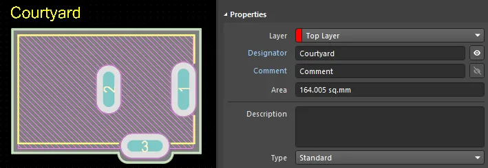
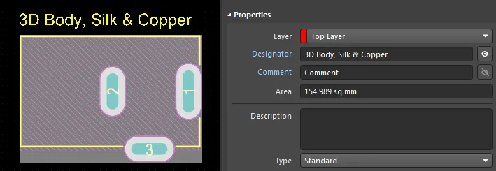
Автоматически вычисляемая площадь — это область, которая подсвечивается при щелчке для выбора компонента. Область выделения определяется по геометрии на слое Courtyard; если этого слоя нет — по совокупности геометрий на слоях Silkscreen, объектов 3D Body и медных слоёв (строки/надписи не учитываются). Верхние изображения ниже показывают площадь компонента, когда контур задан на слое Courtyard; нижнее изображение показывает площадь, когда она вычисляется по геометрии на слоях Silkscreen, 3D Body и Copper.
-
Граница Courtyard проходит по осевой линии контурных треков и дуг, формирующих границу Courtyard.
-
Дуги можно использовать для создания изогнутой формы Courtyard компонента, как показано на верхнем изображении выше, где Courtyard огибает площадку 3.
-
Поле Area отображает площадь выбранного компонента. Если выбрано несколько компонентов, оно покажет площадь одного компонента, если у всех выбранных компонентов площадь одинаковая, либо отобразит *, если значения площади различаются. Чтобы вычислить площадь нескольких выбранных компонентов, используйте панель List panel для отображения площадей этих компонентов. Там можно щёлкнуть правой кнопкой и скопировать значения, затем вставить их в таблицу и вычислить сумму (show image).
► Узнайте больше о том, как вычисляется область выделения и о других режимах, доступных для определения области выделения.
► Узнайте больше о Working with Mechanical Layers.
-
Description – описание этого компонента на уровне компонента. Обычно описание задаётся при создании компонента, но его также можно отредактировать/добавить для компонента на схеме. Это то описание, которое отображается в панели Components panel.
-
Type – выберите здесь один из следующих типов компонента для данного footprint. Доступные типы:
-
Standard – эти компоненты обладают стандартными электрическими свойствами, всегда синхронизируются между схемой и PCB (посадочное место, выводы/площадки и назначения цепей должны совпадать) и включаются в BOM. Пример — стандартный электрический компонент, например резистор.
-
Mechanical – эти компоненты не имеют электрических свойств, не синхронизируются (их нужно размещать вручную в обоих редакторах) и включаются в BOM. Пример — радиатор.
-
Graphical – эти компоненты не имеют электрических свойств, не синхронизируются (их нужно размещать вручную в обоих редакторах) и not включаются в BOM. Пример — логотип компании.
-
Net Tie (in BOM) – эти компоненты используются для замыкания (соединения) двух или более разных цепей между собой. Они всегда синхронизируются между схемой и PCB (посадочное место, выводы/площадки и назначения цепей должны совпадать) и включаются в BOM. Они отличаются от компонента типа Standard тем, что связность, создаваемая медью внутри посадочного места, не проверяется — именно эта медь позволяет замкнуть цепи. Примечание: включите Verify Shorting Copper параметр в диалоге Design Rule Checker, чтобы проверить, что внутри компонента нет несвязанной меди.
-
Net Tie – эти компоненты используются для замыкания (соединения) двух или более разных цепей между собой. Они всегда синхронизируются между схемой и PCB (посадочное место, выводы/площадки и назначения цепей должны совпадать) и not включаются в BOM. Они отличаются от компонента типа Standard тем, что связность, создаваемая медью внутри посадочного места, не проверяется — именно эта медь позволяет замкнуть цепи. Примечание: включите Verify Shorting Copper параметр в диалоге Design Rule Checker, чтобы проверить, что в компоненте нет несвязанной меди.
-
Standard (No BOM) – эти компоненты обладают стандартными электрическими свойствами, всегда синхронизируются между схемой и PCB (посадочное место, выводы/площадки и назначения цепей должны совпадать) и not включаются в BOM. Пример — компонент тестовой точки (testpoint), который вы хотите исключить из BOM.
-
Jumper – эти компоненты используются для добавления перемычек (wire links) в проект PCB, например на односторонней плате, которую невозможно полностью развести в одном слое. Для этого типа компонентов посадочное место и выводы синхронизируются между схемой и PCB, но назначения цепей — нет, при этом компонент включается в BOM. Помимо выбора этой опции на уровне компонента, обе площадки в компоненте должны иметь JumperID, установленный в одно и то же ненулевое значение. Компоненты типа Jumper не обязательно соединять проводниками на схеме; их нужно добавлять на схему только если они требуются в BOM. Если они не требуются в BOM, их можно разместить непосредственно на PCB — при этом задаётся Component Type , задаются JumperIDs , а Nets для площадок назначаются вручную.
-
Design Item ID – отображает Design Item ID для выбранного компонента. Это поле недоступно для редактирования.
-
Source – отображает исходный документ компонента. Нажмите  , чтобы открыть диалог для просмотра и выбора другого исходного документа.
-
Revision State – показывает состояние ревизии компонента библиотек Workspace с точки зрения его состояния жизненного цикла а также статуса ревизии, т.е. является ли это последняя выпущенная ревизия данного компонента (Up to date) или более ранняя ревизия (Out of date).
-
Height – поле высоты компонента. Это поле определяло высоту компонента на плате до появления объекта 3D Body, однако 3D‑модель предоставляет более совершенный способ задания высоты компонента для таких задач, как 3D‑проверка столкновений. Обратите внимание: значение, заданное в этом поле Height, используется Altium MCAD CoDesigner, а не высота 3D‑модели (learn more).
-
3D Body Opacity – введите требуемый процент непрозрачности или используйте ползунок.
-
Primitives – нажмите соответствующий значок замка, чтобы заблокировать/разблокировать.  – заблокировать все примитивы компонента так, чтобы его можно было рассматривать как единый объект.
  – разблокировать, чтобы изменять отдельные примитивы, из которых состоит компонент. После редактирования примитивы компонента следует снова заблокировать.
-
Обратите внимание: когда примитивы компонента заблокированы, большинство их свойств нельзя изменять графическими (например, перетаскиванием) или неграфическими (например, с помощью Properties или панели List ) методами редактирования.
-
Обратите внимание: при необходимости свойства площадок компонента можно открыть и изменить без разблокировки примитивов — для этого дважды щёлкните непосредственно по площадке.
-
Strings – нажмите соответствующий значок замка, чтобы заблокировать/разблокировать. – заблокировать все строки компонента. – разблокировать, чтобы изменять строки компонента.
Выберите кликабельные ссылки Designator и Comment в режиме Component панели Properties, чтобы перейти к соответствующим панелям Properties этих объектов, где можно редактировать их параметры.
Footprint
-
Footprint Name – отображает имя посадочного места, соответствующего выбранному компоненту.
-
Design Item ID – идентификатор выбранного компонента.
-
Source – имя Workspace, в котором был размещён выбранный компонент.
-
Description – описание посадочного места компонента, заданное в редакторе посадочных мест PCB.
Swapping Options
-
Enable Pin Swapping – установите флажок, чтобы разрешить функцию перестановки выводов (pin swapping).
-
Enable Part Swapping – установите флажок, чтобы разрешить функцию перестановки частей (part swapping) (например, четырёх частей микросхемы серии 74).
Schematic Reference Information
При первоначальной передаче проекта справочная информация схемы переносится из редактора схем в редактор PCB. Чтобы обновить эти данные позже, нажмите кнопку Perform Update в диалоге Edit Component Links dialog.
-
Designator – позиционное обозначение (designator) компонента на схеме, с которым был сопоставлен этот компонент PCB.
-
Hierarchical Path – отображает, где в иерархической структуре схемы находится этот компонент.
-
Channel Offset – при первой передаче проекта со схемы на PCB каждому компоненту на каждом листе схемы назначается уникальное смещение канала (channel offset).
Parameters Tab
-
Table – отображает Name, Value и Source для каждого параметра в списке.
Component Designators and Comments
Поля позиционного обозначения (designator) и комментария (comment) являются дочерним объектом параметров компонента PCB (part). Позиционное обозначение используется для уникальной идентификации каждого размещённого элемента, чтобы отличать его от всех остальных элементов, размещённых во всех документах PCB проекта. Комментарий используется для добавления дополнительной информации к размещённому объекту. И комментарий, и позиционное обозначение настраиваются после размещения родительского объекта компонента (part). Это не объект проектирования, который можно разместить напрямую.

Размещённый объект Designator

Размещённый объект Comment
Позиционные обозначения компонентов PCB 2D/3D будут автоматически увеличиваться на единицу при размещении, если исходный компонент имеет обозначение, оканчивающееся числовым символом. Измените обозначение первого компонента до размещения в панели Properties.
Чтобы получить алфавитное или числовое приращение обозначений, отличное от 1, используйте функцию Paste Array. Элементы управления этой функцией находятся в диалоге Setup Paste Array dialog, который открывается нажатием кнопки Paste Array в диалоге Paste Special (Edit » Paste Special).
Графический способ редактирования позволяет выбрать размещённый объект обозначения или комментария непосредственно в рабочей области и изменить его положение, поворот, ориентацию и размер.
Когда выбран объект обозначения или комментария, доступны следующие маркеры редактирования:

Выбранный Designator
-
Щёлкните и перетащите B, чтобы повернуть обозначение/комментарий вокруг его опорной точки A (обозначена маленьким x).
-
Щёлкните и перетащите C, чтобы изменить размер ограничивающей рамки обозначения/комментария одновременно по вертикали и по горизонтали.
-
Щёлкните и перетащите D, чтобы изменить размер ограничивающей рамки обозначения/комментария по вертикали и по горизонтали раздельно.
-
Щёлкните в любом месте обозначения/комментария вдали от маркеров редактирования и перетащите, чтобы переместить его. Во время перетаскивания комментарий можно поворачивать или зеркалировать:
-
Нажмите Spacebar, чтобы повернуть обозначение/комментарий против часовой стрелки, или Shift+Spacebar — по часовой стрелке. Поворот выполняется в соответствии со значением Rotation Step , заданным на странице PCB Editor – General page диалога Preferences.
-
Нажмите клавиши X или Y, чтобы отзеркалить обозначение/комментарий относительно оси X или оси Y.
Свойства объекта Designator или Comment можно изменить в режиме Parameter панели Properties.
Команду
Tools » Add Designators for Assembly Drawing из главных меню можно использовать для автоматического добавления и обновления сборочных позиционных обозначений компонентов на
Designator Component Layer Pair в документе PCB. После запуска команды появится диалоговое окно, в котором будет показано общее количество сборочных позиционных обозначений, которые были добавлены/обновлены. Если документ PCB не содержит
Designator Component Layer Pair, откроется диалоговое окно с предложением добавить Component Layer Pair.
Parameter Properties

Режим Parameter панели Properties.
Location
-
(X/Y)
-
X (первое поле) — текущая координата X (горизонтальная) опорной точки позиционного обозначения относительно текущего начала координат рабочей области. Отредактируйте, чтобы изменить положение позиционного обозначения по X. Значение можно вводить как в метрических, так и в дюймовых единицах; указывайте единицы при вводе значения, если они отличаются от текущих единиц по умолчанию.
-
Y (второе поле) — текущая координата Y (вертикальная) опорной точки позиционного обозначения относительно текущего начала координат. Отредактируйте, чтобы изменить положение позиционного обозначения по Y. Значение можно вводить как в метрических, так и в дюймовых единицах; указывайте единицы при вводе значения, если они отличаются от текущих единиц по умолчанию.
-
Rotation — угол поворота позиционного обозначения (в градусах), отсчитываемый против часовой стрелки от нуля (по 3 o'clock горизонтали). Отредактируйте, чтобы изменить поворот позиционного обозначения. Минимальное угловое разрешение — 0,001°.
Properties
-
Parameter type — отображает тип параметра (Component, Sheet Symbol и т. п.) и имя параметра.
-
Name — имя позиционного обозначения.
-
Value — используйте это поле, чтобы ввести требуемое значение позиционного обозначения. Нажмите значок «глаз», чтобы переключать отображение значения: видно/не видно в области проектирования.
Отображение позиционного обозначения или комментария для размещённого компонента можно переключать между «не скрыто» и «скрыто», щёлкнув компонент правой кнопкой мыши в области проектирования и выбрав в контекстном меню команду
Component Actions » Hide Designator /
Component Actions » Show Designator или
Component Actions » Hide Comment /
Component Actions » Show Comment соответственно.
-
Layer — используйте выпадающий список, чтобы выбрать нужный слой. При необходимости включите Mirror .
-
Autoposition — используйте выпадающий список, чтобы выбрать требуемое автоматическое положение относительно связанного объекта.
-
Text Height — используйте это поле, чтобы задать требуемую высоту текста.
-
Font Type
-
TrueType — выберите, чтобы использовать шрифты, доступные на вашем ПК (в папке \Windows\Fonts ). Шрифты TrueType обеспечивают полную поддержку Unicode. По умолчанию ПО ссылается на используемый шрифт TrueType (они не сохраняются в файле PCB), а это означает, что один и тот же шрифт должен присутствовать на каждом ПК, на который переносится проект. Либо можно внедрить используемые шрифты TrueType в файл PCB с помощью параметров на странице PCB Editor - True Type Fonts диалога Preferences , где также можно выбрать Substitution Font , который будет использоваться, если невстроенный шрифт недоступен.
-
Justification — используйте, чтобы задать расположение позиционного обозначения внутри прямоугольной рамки.
-
Left (
 ) — нажмите левую кнопку, чтобы выровнять горизонтальный текст по левому краю.
-
Center (
 ) — нажмите центральную кнопку, чтобы выровнять горизонтальный текст по центру.
-
Right (
 ) — нажмите левую кнопку, чтобы выровнять горизонтальный текст по правому краю.
-
Above (
 ) — нажмите верхнюю кнопку, чтобы выровнять вертикальный текст по верхнему краю.
-
Middle (
 ) — нажмите среднюю кнопку, чтобы выровнять вертикальный текст по середине.
-
Below (
 ) — нажмите нижнюю кнопку, чтобы выровнять вертикальный текст по нижнему краю.
-
Font — используйте выпадающий список, чтобы выбрать нужный шрифт TrueType. Используйте параметры B (bold) и/или I (italic) для выделения текста по необходимости.
-
Inverted — используйте , чтобы отображать текст инвертированным с возможностью управления размером рамки вокруг текста. Для дополнительной настройки текста можно использовать следующие параметры:
-
Size (Width/Height) —
-
Width — ширина прямоугольной рамки.
-
Height — высота прямоугольной рамки.
-
Stroke
-
Justification — используйте, чтобы задать расположение позиционного обозначения внутри прямоугольной рамки.
-
Left () — нажмите левую кнопку, чтобы выровнять горизонтальный текст по левому краю.
-
Center () — нажмите центральную кнопку, чтобы выровнять горизонтальный текст по центру.
-
Right () — нажмите левую кнопку, чтобы выровнять горизонтальный текст по правому краю.
-
Above () — нажмите верхнюю кнопку, чтобы выровнять вертикальный текст по верхнему краю.
-
Middle () — нажмите среднюю кнопку, чтобы выровнять вертикальный текст по середине.
-
Below () — нажмите нижнюю кнопку, чтобы выровнять вертикальный текст по нижнему краю.
-
Font — используйте выпадающий список, чтобы выбрать нужный Stroke-шрифт. Варианты:
-
Default — простой векторный шрифт, предназначенный для перьевой и векторной фотоплоттерной печати.
-
Sans Serif — сложный шрифт, который замедляет формирование векторного вывода, например Gerber.
-
Serif — сложный шрифт, который замедляет формирование векторного вывода, например Gerber.
-
Stroke Width — отображает ширину штриха.
-
Border Mode
-
Margin — нажмите эту кнопку, чтобы включить редактирование параметра Margin Border.
-
Text Offset — величина, на которую позиционное обозначение смещается внутрь от края/угла, относительно которого выполняется выравнивание. Этот параметр не влияет на результат, когда выбран режим выравнивания Center . Этот параметр недоступен для Margin.
-
Offset — нажмите эту кнопку, чтобы включить редактирование параметра Text Offset.
-
Margin Border — используйте, чтобы задать размер поля (margin border), окружающего позиционное обозначение. Этот параметр недоступен для Offset.
Доступность компонентов на PCB
Когда проект передаётся из редактора схем в редактор PCB, посадочные места компонентов PCB автоматически размещаются из доступных библиотек. Это называется Design Synchronization — процесс обнаружения и устранения различий между схемой и PCB.
Altium Designer поддерживает набор инструментов, упрощающих размещение требуемого посадочного места компонента в области проектирования PCB. См. следующие страницы, чтобы узнать об этих инструментах:
Просмотр размещённых компонентов
В режиме PCB panel’s Components три основные области панели изменяются, чтобы отражать иерархию компонентов текущего проекта PCB (сверху вниз):
-
Component Classes
-
Components внутри класса
-
Component Primitives

Области панели PCB позволяют выполнять накопительный выбор фильтра: от классов компонентов к отдельным компонентам и далее к примитивам компонентов.
Щёлкните правой кнопкой по записи компонента или примитива компонента и затем выберите команду Properties (или дважды щёлкните по записи), чтобы открыть панель Properties, где можно просматривать/изменять свойства компонента/примитива по необходимости.
Щёлкните правой кнопкой по записи класса компонентов и затем выберите Properties (или дважды щёлкните по записи), чтобы открыть диалог Edit Component Class dialog для этого класса. В диалоге можно просматривать/изменять состав класса, переименовывать его или добавлять дополнительные классы.

Редактирование выбранного класса компонентов.
Отображение/включение каждого типа примитивов компонента в области Component Primitives панели зависит от того, включён ли соответствующий параметр для каждого типа в меню правой кнопки мыши, доступном из областей Components или Component Primitives.

Щёлкните правой кнопкой по записи компонента или примитива компонента, чтобы выбрать элементы для включения.
Во время просмотра компоненты можно легко блокировать или разблокировать, дважды щёлкнув в поле справа от столбца Footprint в области Components.
Блокировка/разблокировка из панели PCB избавляет от необходимости переходить в панель Properties.
Ограничивающий прямоугольник выбора компонента
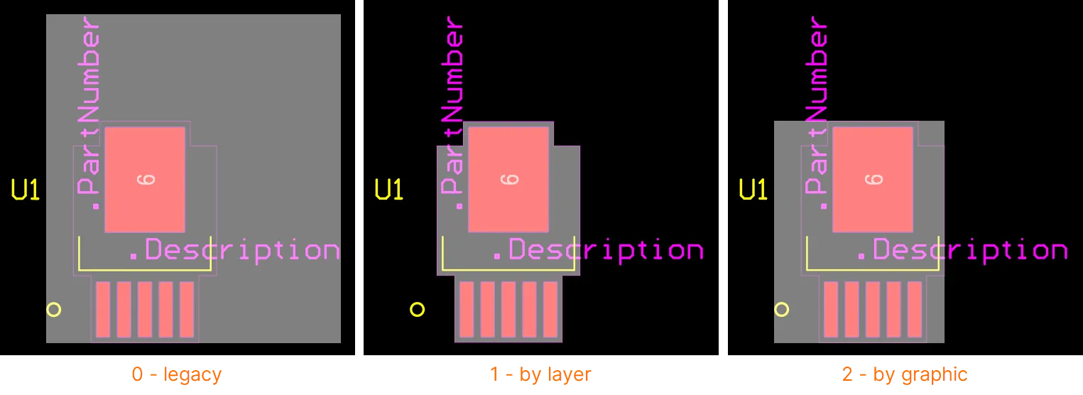
Когда вы щёлкаете и выбираете компонент, появляется ограничивающий прямоугольник выбора. Чтобы управлять тем, какие слои используются для определения этого прямоугольника, можно использовать параметр PCB.ComponentSelection в диалоге Advanced Settings dialog . Параметр поддерживает три режима (введите значение 0, 1 или 2; режим по умолчанию — 2):
-
0 - legacy mode — этот режим объединяет геометрию со всех слоёв, кроме строк Silkscreen Designator и Comment.
-
1 - by layer mode — использовать геометрию первого из перечисленных ниже слоёв, который содержит объекты, со следующим приоритетом:
-
Тип слоя Courtyard
-
Слой 3D Body (модели STEP хранятся в объекте 3D Body, размеры которого соответствуют наименьшему прямоугольному параллелепипеду, вмещающему модель. Для выбора компонента используется именно этот 3D Body, а не форма STEP‑модели)
-
Слой шелкографии плюс медные слои
-
Медные слои
-
2 - by graphic mode - этот режим объединяет геометрии, обнаруженные по типу слоя Courtyard, на шелкографии, в объектах 3D Body и на медных слоях. Строки (текст) исключаются.
-
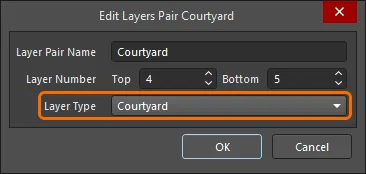
Ссылки на слой Courtyard относятся к паре слоёв компонента (Component Layer Pair) с Layer Type = Courtyard; имя пары слоёв не учитывается.
-
Если компонент включает 3D‑модель, для проверки столкновений компонентов используется фактическая форма 3D‑модели, тогда как форма рамки выбора компонента определяется, как описано выше.
-
Объекты механических слоёв исключаются из ограничивающей рамки выбора, но включаются в ограничивающую рамку проверки столкновений, когда не определены 3D Body или объекты на слое Courtyard. Исключение составляют текстовые строки .Designator и .Comment, которые всегда исключаются. Подробнее см. Working with Mechanical Layers.
-
Когда ограничивающая рамка выбора компонента задаётся дорожками на слое courtyard, для определения рамки используется осевая линия этих дорожек (как видно при выборе компонента — 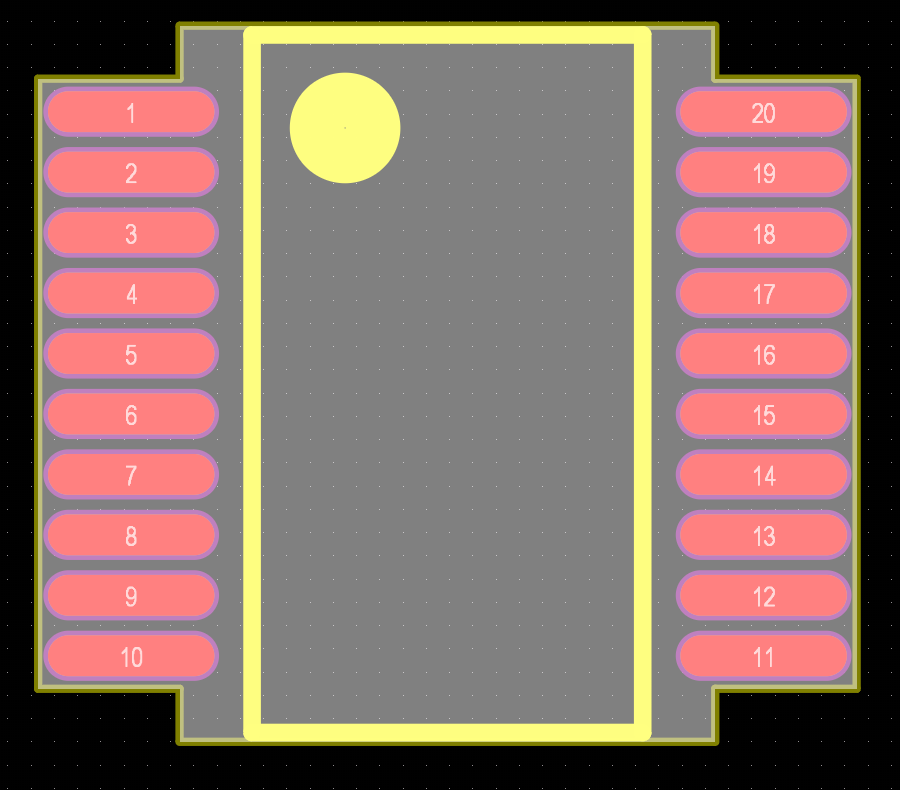 ). Обратите внимание: это справедливо только в случае, когда форма, заданная на слое courtyard, является замкнутой, а конечные вершины дорожек совпадают (точно соприкасаются). В противном случае ограничивающая рамка определяется как наименьший прямоугольник, охватывающий все объекты на слое courtyard.
-
Ограничивающая рамка выбора компонента используется для расчёта площади компонента и при размещении компонентов в режимах размещения препятствий Push и Avoid placement modes.
Добавление примитивов в компонент
Выбранные примитивы можно добавить в компонент, выбрав команду Tools » Convert » Add Selected Primitives to Component в главном меню. После выбора команды укажите компонент, в который нужно добавить выбранные примитивы. После подтверждения новые примитивы будут распознаны как часть единого объекта компонента и могут использоваться совместно с исходными примитивами компонента.
Для выполнения этой операции целевой компонент должен иметь разблокированные примитивы. Используйте значок замка Primitives в свойствах компонента, чтобы разблокировать примитивы компонента.
Разбиение компонента на примитивы
Компонент можно преобразовать в составляющие его примитивные объекты с помощью команды Tools » Convert » Explode Component to Free Primitives из главного меню или щёлкнув правой кнопкой мыши по размещённому компоненту (выбранному или нет) и затем выбрав команду Component Actions » Explode Component To Free Primitives (или Explode Selected Components To Free Primitives) в контекстном меню. Разбитый компонент перестаёт быть компонентом, поэтому обозначение (designator) и комментарий будут удалены, а компонент вернётся к набору примитивов, из которых он был собран.
Команда Explode не влияет на модель посадочного места, хранящуюся в соответствующей исходной библиотеке, а только на преобразованные экземпляры компонента(ов), размещённые в документе PCB.
-
Explode — необратимый процесс; команды для повторной группировки разбитого компонента нет. Однако для этого можно использовать команду Undo.
-
Команду Explode не следует использовать для изменения свойств компонента. Примитивы компонента можно редактировать, разблокировав их (с помощью значка замка Primitives в свойствах компонента), внеся необходимые изменения и затем снова заблокировав их.
Доступ к кликабельным ссылкам на справочную информацию
Если в компонент добавлены именованные ссылки на документы, можно открыть указанный URL документа/страницы — заданный через определённый базовый параметр URL‑ссылки — для выбранного компонента или компонента под курсором. Эта функция позволяет отображать именованные ссылки на документы, перенесённые из компонентов схемы, как именованные ссылки PCB‑компонента на PDF, текстовые файлы или HTML‑страницы. Это происходит, когда именованные ссылки на документы для компонента были обновлены из схемы в PCB (Design » Update PCB Document). В процессе обновления (через ECO) именованные ссылки схемы преобразуются в пары параметров ComponentLink (ComponentLinknDescription/ComponentLinknURL) для соответствующего PCB‑компонента. Например:
| Параметр компонента схемы |
|
Параметры PCB‑компонента |
| Name |
Url |
⇒
|
Name |
Value |
STM32 Family Web Page |
http://www.st.com/stm32 |
ComponentLink1Description |
STM32 Family Web Page |
ComponentLink1URL |
http://www.st.com/stm32 |
Номер индекса ссылки (n), используемый в параметрах компонента, определяет упорядоченную позицию соответствующей PCB Component Link в подменю References. При выбранном компоненте на PCB определённые пары параметров ComponentLink отображаются в разделе Parameters панели Properties panel.
После запуска команды целевая веб‑страница по URL или указанный документ откроется напрямую (если доступно).
-
Веб‑URL будет открыт либо во внешнем браузере, либо как документ во вкладке внутри Altium Designer — в зависимости от параметра Open internet links in external Web browser на странице System - View page диалога Preferences. Учтите: чтобы открыть во внешнем браузере, значение (URL) параметра ссылки должно включать префикс http://.
-
Подробнее о создании параметров ссылок на документы в пространстве схемы см. на странице Schematic Libraries.


 Локализовано с помощью ИИ