
Altium Designer の新機能
このページでは、Altium Designer、Altium Designer Develop、Altium Designer Agile の将来的なバージョンに含まれる改善点について説明します。各更新には、既存のテクノロジーを発展させ成熟させる様々な改善を提供すると共に、AltiumLive コミュニティの BugCrunch システムを通じてお客様から寄せられたフィードバックに基づいてソフトウェア全体に渡る多くの修正と機能強化も組み込まれており、最先端のエレクトロニクス テクノロジーの開発を継続できるように支援します。
バージョン 26.3
Altium Designer Develop – リリース日: 2026年2月5日 – バージョン 26.3.0 (build 5)
Altium Designer Agile – リリース日: 2026年2月5日 – バージョン 26.3.0 (build 18)
Altium Designer – リリース日: 2026年2月5日 – バージョン 26.3.0 (build 6)
PCB デザインの改善
SOLIDWORKS、および Parasolid 形式の対応を強化
-
3D 外形 で作業する時、SOLIDWORKS 2024、および 2025 モデル (
*.SldPrt) を対応しました。 -
PCB を Parasolid ファイル形式 (
*.x_t) でエクスポートする際に、Parasolid バージョン 35.1 が使用されるようになりました。これにより、SOLIDWORKS の最新バージョン (2024 と 2025) でファイルを正しく開いたりインポートできます。
詳細については、Mechanical Data Import-Export Support のページをご参照ください。
ハーネスデザインの改善
ジャンパワイヤの表示
wiring diagram で定義されたジャンパワイヤが、関連する layout drawing に正しく配置されるようになりました。ジャンパワイヤは、同じコネクタの 2 つの cavity を接続します。layout drawing でバンドルを選択すると、Properties パネルの Bundle Objects 領域に、同じ接続点で開始、および終了するジャンパワイヤがそのバンドルの一部として含まれるようになりました。
このようなワイヤの長さは、手動でのみ定義できます。入力された値は、ハーネスプロジェクトの ActiveBOM ドキュメントと製造図 (BOM table と wiring list) に含まれます。
このハーネスデザインの例では、ワイヤ W7 は wiring diagram 内の同じコネクタ (P3) の cavity を接続するため、ジャンパワイヤと見なされます。
デザインの layout drawing では、ワイヤ W7 は P3 へ接続されたバンドルのバンドルオブジェクトとしてリスト表示されます。
詳細については、Creating the Layout Drawing のページをご参照ください。
'Update From Libraries' 機能の改善
ハーネスデザインの wiring diagrams (*.WirDoc) と layout drawings (*.LdrDoc) のライブラリからの更新 (Tools » Update From Libraries) を改善しました。
-
wiring diagram からこの機能を実行した時、ワイヤ、cavity コンポーネント、および関連部品も含まれるようになりました。

-
layout drawing からこの機能を実行した時、ハーネスカバー、レイアウトラベル、および関連部品も含まれるようになりました。

詳細については、Defining the Wiring Diagram と Creating the Layout Drawing のページをご参照ください。
プラットフォームの改善
EULA を Master Services Agreement に変更
Altium Designer Develop、または Altium Designer Agile のインストール時に、End User License Agreement (EULA) を Master Services Agreement (MSA) に変更しました。
詳細については、Installing & Managing Altium Designer Develop と Installing & Managing Altium Designer Agile のページをご参照ください。
バージョン 26.2
Altium Designer Develop – リリース日: 2026年1月8日 – バージョン 26.2.0 (build 10)
Altium Designer Agile – リリース日: 2026年1月8日 – バージョン 26.2.0 (build 28)
Altium Designer – リリース日: 2026年1月8日 – バージョン 26.2.0 (build 7)
ワイヤボンディングの改善
面付け PCB の対応
面付け PCB ドキュメントを 3D で表示する時、ボンドワイヤとダイパッドが表示されるようになりました。

また、面付け PCB ドキュメントからの Wire Bonding Table Report の生成も対応するようになりました。
面付け PCB の詳細については、Board Panelization のページをご参照ください。
ボンドワイヤを検出するための新しいクエリ キーワード
PCB/PcbLib 内のオブジェクトのフィルタリング、またはデザインルールのスコープ設定で使用する論理クエリ式を構築する時、新しい IsBondwire クエリ キーワード (PCB Object Type Check) を利用できます。

詳細については、Object Type Checks のページをご参照ください。
ハーネスデザインの改善
ハーネスバンドルの Break Point を配置する機能
harness layout drawing (*.LdrDoc) 内のハーネスバンドルに、バンドルが非縮尺 (Not to Scale (NTS)) であることを示すために使用される break point を配置できるようになりました。バンドルには、以下の最初の画像に示す様に、最長セグメントの中央に break symbol が表示され、properties には、デザインスペースで描画されたバンドルの長さを反映する Drawn Length が表示されます。通常、物理的なバンドルの長さはかなり長くなります。Length 欄 (実際の物理的な長さ) が設定されていて、描画された長さと異なる時、バンドルが非縮尺 (Not to Scale (NTS)) であることを示すために、バンドルの最長セグメントの中央に break symbol が表示されます。break を配置するには、bundle properties の Properties 領域で Add Break Symbol オプションを有効にします。break point のあるハーネスバンドルを覆うハーネスカバーにも、同じ場所に break が表示されます。ハーネスカバーがハーネスバンドルの break point で終了する場合、2 番目の画像に示す様に、カバーは少し長く描画されます。
バンドル上に配置した break point
配置された break point 上に配置されたカバー
詳細については、Creating the Harness Layout Drawing のページをご参照ください。
データ管理の改善
コンポーネントを同期する時にライフサイクル状態を保持する機能
このバージョンでは、Altium Designer の Components Synchronization 機能を使用して、Workspace とコンポーネント データベース間でコンポーネントの同期を実行する時、ライフサイクル状態を保持できるようになりました。
この機能は、新しい Preserve lifecycle state オプションで実行します。Components Synchronization Configuration ドキュメント (*.CmpSync) でデータソース (table) を選択すると、Properties パネルの Advanced の項目にこのオプションが表示されます。

この機能は、Allow to skip lifecycle state change for new revisions 操作権限 (詳細は、Setting Global Operation Permissions for a Workspace をご覧ください) が割り当てられているユーザが利用できることに注意してください。
Components Synchronization 機能の詳細にいては、Component Database to Workspace Data Synchronization のページをご参照ください。
Altium Designer 26.2 で完全に公開された機能
以下の機能は、このバージョンで正式に公開されるようになりました:
-
BOM CoDesign - 25.1 から利用可能
-
Excluding Supplier-related Fields from BOM Comparison Result - 26.1 から利用可能
バージョン 26.1
Altium Designer Develop – リリース日: 2025年12月3日 – バージョン 26.1.0 (build 6)
Altium Designer Agile – リリース日: 2025年12月3日 – バージョン 26.1.0 (build 13)
Altium Designer – リリース日: 2025年12月3日 – バージョン 26.1.0 (build 7)
PCB デザインの改善
Solder Mask Expansion ルールのデフォルトを 0 ミルに設定 (Open Beta)
パッドスタックのデフォルトに関して IPC-7351B 規格を遵守すると、solder mask の開口は通常、ランドサイズの 1:1 の比率であり、Solder Mask Expansion ルール (PCB ドキュメント内) とルール駆動の solder mask expansion (PCB ライブラリ ドキュメント内) の値は、デフォルトで 0 mil (以前は 4 mil) に設定されるようになりました。
PCB ライブラリ (*.PcbLib) の場合、これらの新しいデフォルト値の対応はライブラリレベルであり、そこに作成された全てのコンポーネント フットプリントで継承されます。以下のパッドオブジェクトに示す様に、同じ PCBlib では、全てのオブジェクトのルール駆動の solder mask expansion について、Altium Designer の以前のバージョンで開口した場合は 4 ミルの開口が表示され、このバージョン以降で開いた場合は 0 ミルの開口が表示されます。

PCB ドキュメント (*.PcbDoc) の場合、既存の Solder Mask Expansion ルールは、初期値が保存されます。新しく作成されたルールに使用されるデフォルト値は、そのルールが作成された Altium Designer のバージョンによって決定され、別のバージョンの Altium Designer で開いている間は変更されません。従って、以下に示す様に、Altium Designer の以前のバージョンで作成され、他のバージョンで開いた場合、デフォルトは 4 ミルの開口となり、このバージョン (または、それ以降) で作成され、他のバージョンで開いた場合、デフォルトは 0 ミルの開口になります。

Constraint Manager で新しく作成された Solder Mask Expansion デザインルール。

PCB Rules and Constraints Editor ダイアログで新しく作成された Solder Mask Expansion デザインルール。
Solder Mask Expansion デザインルールの詳細については、Mask Rule Types のページをご参照ください。
制約マネージャの改善
クラスをフィルタリングする機能を追加
クラスをフィルタリングする機能を制約マネージャの Clearances ビューに実装し、多数のクラスの作業を活用できるようになりました。これにより、クラスのフィルタ (または、グループ化) を構築して、clearances matrix のフォーカスしたサブセット間で切り替えたり、サブセットで作業できます。
Clearances ビューの右上にある ![]() ボタンを使用してポップアップにアクセスし、フィルタの作成、編集、削除、有効化/無効化を行うことができます。
ボタンを使用してポップアップにアクセスし、フィルタの作成、編集、削除、有効化/無効化を行うことができます。
![]()
新しいフィルタを作成するには、![]() ボタンをクリックし、表示されるポップアップの
ボタンをクリックし、表示されるポップアップの ![]() ボタンをクリックします。
ボタンをクリックします。
![]()
新しいフィルタの固有の名称を定義し、必要なクラスのグループを有効にして、![]() をクリックします。
をクリックします。
![]()
フィルタを作成したら、ポップアップで利用できるコントロールを使用して、必要に応じて、フィルタを有効、無効、編集、または削除します。フィルタが有効の場合、右上のボタンは ![]() として表示されることに注意してください。
として表示されることに注意してください。
clearance matrix での作業の詳細については、Defining Design Requirements Using the Constraint Manager のページをご参照ください。
Draftsman の改善
Draftsman ドキュメントへの DXF インポートの強化 (Open Beta)
この機能により、DXF ファイルバージョン R12 以降を製造図ドキュメント (*.PCBDwf、*.HarDwf、*.MbDwf) へインポートできます。スプラインを含む DXF ファイルのインポートも対応するようになりました。
DXF ファイルのインポートの詳細については、Draftsman Placement & Editing Techniques のページをご参照ください。
ワイヤボンディングの改善
パネル内のボンドワイヤ プリミティブ
以下の箇所で、ボンドワイヤが正しいタイプ (Bond Wire) で表示されるようになりました:
-
PCB パネルの Nets モード での Primitives 領域 (選択したネットのコンポーネントに関する)。
-
PCB パネルの Components モード での Component Primitives 領域 (選択したコンポーネントのネットに関する)。
-
PCB Library パネル (選択したフットプリントに関する)。
ボンドワイヤ プリミティブを選択すると、デザインスペース内でそのボンドワイヤが選択/ハイライト表示されます。


更に、領域を右クリックして表示されるコンテキストメニューに Show Bond Wires オプションを追加し、ボンドワイヤの表示/非表示を切り替えることができるようになりました。
ワイヤボンディングの詳細については、Wire Bonding のページをご参照ください。
3D-MID デザインの改善
3D-MID デザインルールチェック (Open Beta)
このバージョンでは、3D 基板上の配線済みトラックの Width、Clearance、Length、Matched Lengthsルール違反を検出するバッチ Design Rule Checking (DRC) 機能を追加しました。生成される DRC レポートにはこれら全てのチェック情報が含まれますが、デザインスペース内では clearance 違反のみがハイライト表示されることに注意してください。


詳細については、3D-MID Design のページをご参照ください。
マルチボードデザインの改善
ハーネスエントリの 'Termination Type' を定義する機能
マルチボード回路図で、ハーネスエントリの Termination Type を定義できるようになりました。利用できる termination type は以下です:
-
Connector – PCB 上の mating connector へ接続する時に使用する標準のオプションです。通常は、標準の基板実装コネクタを使用します。
-
Crimps/Ferrules – 個々のワイヤは、PCB 側のコネクタへ挿入される前に、crimps、または ferrules で終端されます。
-
Wire termination – ハーネス端のワイヤは鈍角に切断され、PCB へ直接、ネジ止め、またははんだ付けされます。これは、一部の JST コネクタ等のワイヤと基板を直接、接続する場合に一般的です。
選択したハーネスエントリと対応するモジュールエントリのプロパティにその情報が反映されます。


マルチボード回路図における接続作業の詳細については、Working with Connections のページをご参照ください。
ハーネスデザインの改善
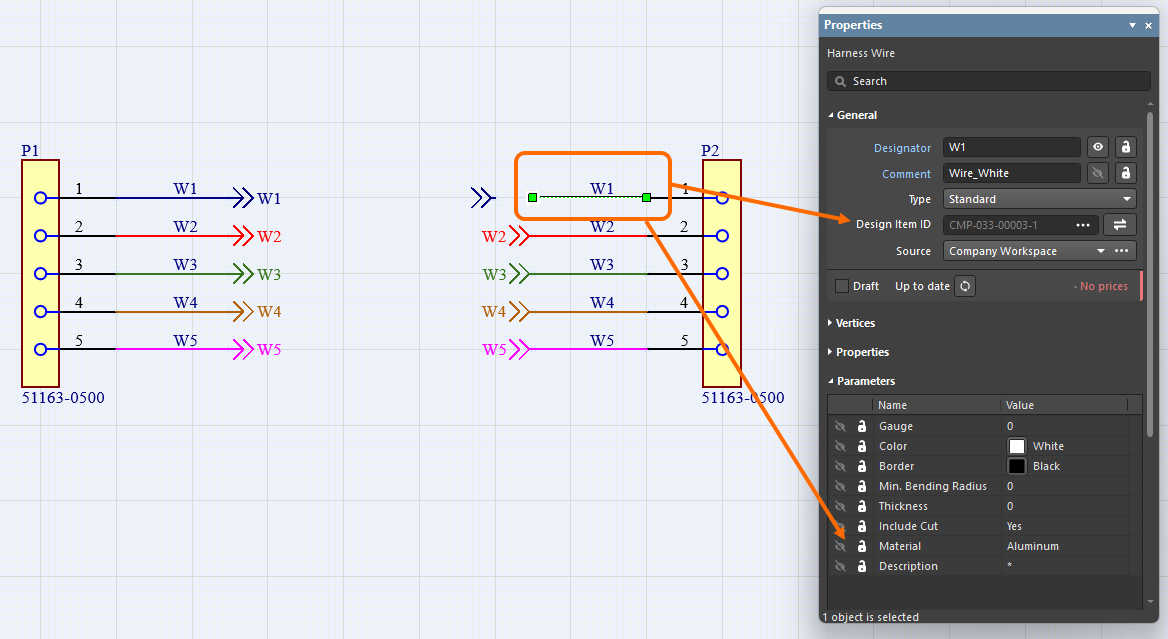
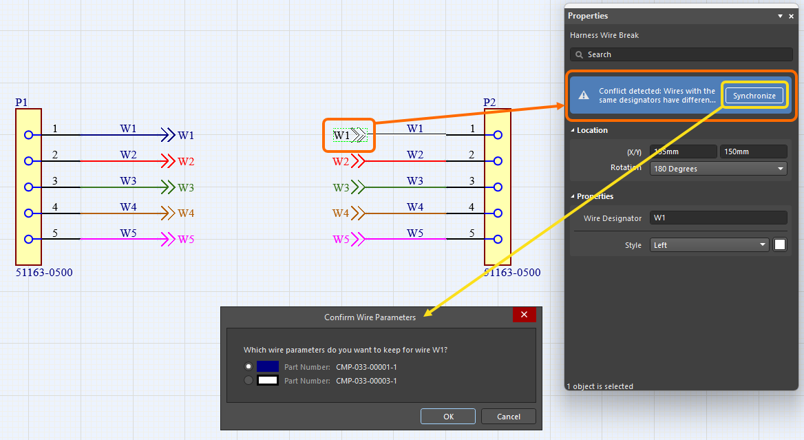
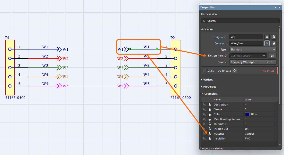
ワイヤの同期を強化
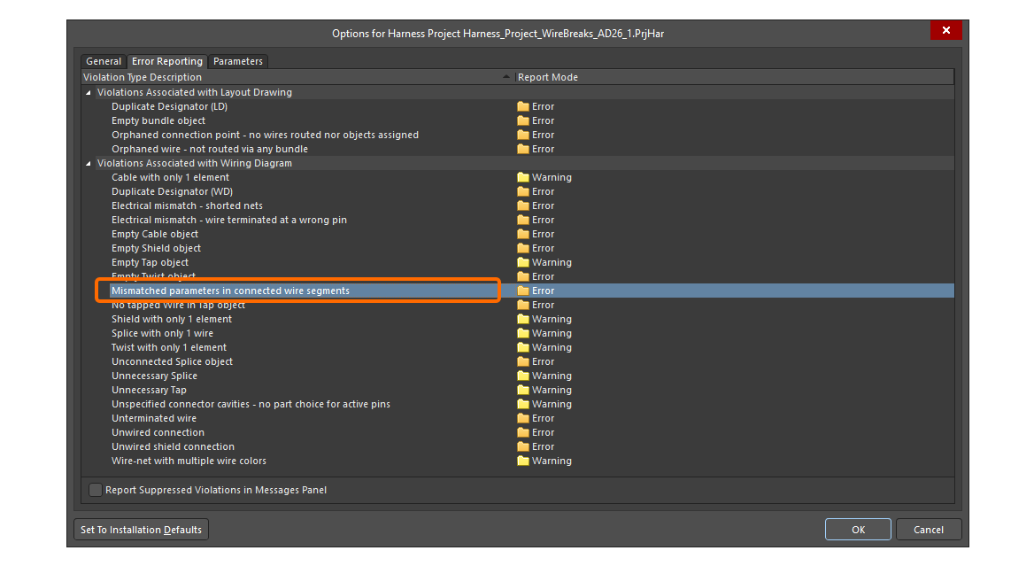
wire break で接続されたハーネスワイヤは、Design Item ID が異なっていても認識されるようになりました。更に、同じ wire break で接続された、同じデジグネータの全てのワイヤセグメントが比較されるようになりました (part number、comment、color、全てのパラメータ)。相違が見つかった場合、Mismatched parameters in connected wire segments の違反がレポートされます。また、ワイヤと wire break の Properties パネルに、パラメータ間で不一致が検出されたことを示す警告が表示されます。警告内で Synchronize をクリックすると、Conflict Wire Parameters ダイアログが開き、ワイヤセグメントに使用するパラメータを選択できます。
ジャンクションポイント上にカバーを配置する機能
ハーネスレイアウト図 (*.LdrDoc) でジャンクションポイント (layout drawing 内で 2 つ以上のバンドルが結合する接続点) 上にハーネスカバーを適用/拡張できるようになりました。これにより、複数のコネクタを含むセクション内のジャンクションポイント間に個別のハーネスカバーを設定する必要がなくなります。

更に、カバーの開始点は経路の最左上点として扱われるようになり、その経路にはカバーが配置されているバンドルのみが含まれるようになりました。
詳細については、Creating the Layout Drawing のページをご参照ください。
特定のオブジェクトについて、BOM の Quantity 欄を 'As Required' へ変更
ワイヤ、ケーブル、ハーネスカバーは長さベースのオブジェクトであり、値は Length 欄に表示されます。混乱を避けるため、Bill Of Materials テーブル、および製造図ドキュメント (*.HarDwf) のActiveBOMドキュメントにおける wire、cable、harness covering エントリの Quantity 欄は、As Required に変更しました。

詳細については、Managing Your Bill of Materials (BOM) with ActiveBOM のページをご参照ください。
Wiring List のピングループ化の改善
ハーネス製造ドキュメント (*.HarDwf) に配置された wiring list におけるピンのグループ化を改善しました。このバージョン以降、下図に示す様に、最も多くのワイヤを持つコネクタへ自動グループ化が適用され、その全ての cavity が wiring list の From 列に正しくグループ化されます。

ハーネスメーカーのための Excel Workbook
ハーネスメーカーが使用するデータを含む単一の Excel Workbook を、出力ジョブを通じて生成する機能を追加しました。この機能を容易にするために、Report Outputs の項目に新しい出力機能 Manufacturing Data を追加しました。

生成された Workbook には、以下の 4 つの個別のシートが含まれます:
-
Bill of Materials – 迅速な見積り作成に役立ちます。
-
Wiring List – ワイヤ加工機用。
-
Labels – Zebra、またはその他のプリンタで使用するために、ハーネスバンドルに印刷する物理的なラベルの概要。
-
Coverings – ハーネスバンドルに適用されるカバーの概要。


詳細については、Preparing Reports のページをご参照ください。
プラットフォームの改善
.NET 8 への切り替え
このバージョンでは、Altium Designer は .NET 6 から .NET 8 の使用に切り替わります。これは、Altium Designer の一部としてバンドルされており、一般的なパフォーマンス強化を含む、.NET の最新の機能と開発を活用できるようになります。
詳細については、System Requirements のページをご参照ください。
WebView2 (Open Beta)
このバージョンから、Altium Designer 内のブラウザ関連要素 (例えば、Home ページ) に WebView2 が使用されます。これにより、Windows を更新するだけで、Altium Designer 内で最新の Web ブラウザエンジンへアクセスできます。
データ管理の改善
プロセスワークフローを使用して Workspace プロジェクトをコピーする機能
定義済み (かつ、有効化済み) のプロセスワークフローを使用して、Workspace プロジェクトのコピーを作成するための機能を追加しました。Workspace プロジェクトを開いた時、Projects パネルでプロジェクトエントリを右クリックし、Make a copy of the managed project サブメニューから有効化されたプロセス定義 (Project Creations テーマの一部) を選択して、そのプロセスの基礎となるワークフローに従ってプロジェクトのコピーを開始できます。

詳細については、Process-based Project Creation のページをご参照ください。
モデルをリリースする時にライフサイクル状態を保持する機能を追加
コンポーネントモデル (回路図シンボル、PCB フットプリント、シミュレーションモデル、または ハーネス配線) の新しいレビジョンを接続された Workspace へリリースする時、モデルの現在のライフサイクル状態を保持できるようになりました。

この機能は、Allow to skip lifecycle state change for new revisions 操作権限 (詳細は、Setting Global Operation Permissions for a Workspace をご欄ください) が割り当てられているユーザが利用できることに注意してください。
Workspace 内容の編集の詳細については、Creating & Editing Content のページをご参照ください。
デザインレビューでのコメントのリンク
デザインレビューの一部としてコメントが追加された時、そのレビューへのリンク (From <DesignReviewName>) が、Comments And Tasks パネルの対応するエントリ内と、そのコメントのコンテキストコメント ウィンドウ (デザインスペース内) 内に表示されるようになりました。リンクをクリックすると、デフォルトブラウザの新しいタブでレビューの Overview ページが開きます。

ドキュメントへのコメントの詳細については、Document Commenting のページをご参照ください。
追加の Unit-aware データタイプの対応
Altium プラットフォーム上の接続された Workspace でコンポーネント テンプレートの一部としてユーザパラメータを定義する時、以下の追加の unit-aware データタイプを対応するようになりました:
-
Area (mm2)
-
Bar (bar)
-
Bit
-
Candela (cd)
-
Decimal
-
Integer
-
Joule (J)
-
Lumen (lm)
-
Millimetre (mm)
-
Pascal (Pa)
-
Pounds per square inch (psi)
-
Rotations per minute (rpm)
-
Siemens (S)
-
Tesla (T)

これらの新しい単位タイプを使用するパラメータは、Components パネル、Component エディタ (single と batch 編集モードの両方)、Library Importer と Components Synchronization 機能 (Properties パネルの Parameter Mapping の項目内) を含む、ソフトウェアの様々な領域で対応しています。
unit-aware コンポーネント パラメータのデータタイプの詳細については、Component Templates のページをご参照ください。
Components Synchronization の使用時に Part Choices を同期する機能
Components Synchronization 機能と、関連する Components Synchronization Configuration ドキュメント (*.CmpSync) を使用して、part choice 情報を定義、および同期する機能を追加しました。同期されたパラメータのコントロールは、ドキュメントでテーブルを選択する時、Properties パネルの Part Choices Mapping 領域で利用できます。part choice パラメータのペア (Manufacturer / Part Number) を追加、削除するボタンやドロップダウンメニューオプションを使用して、マッピングを定義できます。マッピングが定義されると、対応するパラメータがドキュメントリストの Part Choice n 列に表示されます。

Components Synchronization 機能の詳細については、Component Database to Workspace Data Synchronization のページをご参照ください。
Workspace への接続の問題に関する新しい警告
Workspace への接続に問題があり、プロジェクトドキュメントの最新の VCS 状態を更新できない場合、Projects パネルのプロジェクトエントリの横に Refresh VCS Statuses コントロール (関連するツールチップ警告付き) が表示されるようになりました。接続が再開したら、エントリをクリックすると VCS 状態が再び同期され、最新の変更内容が表示されます。

ドキュメントの状態を示す方法の詳細については、Managing Project Documents のページをご参照ください。
BOM CoDesign の改善
BOM 比較結果からサプライヤー関連欄を除外 (Open Beta)
BOM CoDesign 機能を使用して ActiveBOM と、管理された BOM を比較する場合、advanced setting が無効になっていると、ActiveBOM ドキュメントからアクセスした時、Properties パネルの Related BOMs タブの Differences section からサプライヤー関連データ (Supplier と Supplier Part Number パラメータ) が除外されます。


比較結果の調査の詳細については、BOM CoDesign のページをご参照ください。
インポート/エクスポートの改善
Allegro Design のインポートを強化
必要な全ての設定ファイルは、Allegro2Altium.bat ファイルに含まれるようになりました。このバッチファイルは、Altium Designer インストールに含まれており、Allegro バイナリ (*.brd 、または *.dra) ファイルを ASCII 形式へ変換するために使用されます (そのようなデザイン/ライブラリが Altium Designer と同じ PC 上に無い場合)。従って、インポートには bat ファイルのみが必要で、追加のファイルは必要ありません。
比較結果の調査の詳細については、Importing a Design from Allegro のページをご参照ください。
xDX Designer デザインからのコンポーネント Alternative 表示の対応
xDX Designer デザインをインポートする時、生成された回路図と回路図ライブラリ ドキュメントの両方で、コンポーネントの Alternate 表示モードを対応するようになりました。
比較結果の調査の詳細については、Importing a Design from xDX Designer or DxDesigner のページをご参照ください。
Altium Designer 26.1 で完全に公開された機能
以下の機能は、このバージョンで正式に公開されるようになりました:
-
Detailed Pad Stack for Allegro Imports - 25.7 から利用可能
-
Properties Panel Optimization for PCB Object Properties - 25.7 から利用可能
Altium Designer 26.1 のその他の機能
-
Hidden Links to External VCS Repositories (Open Beta): このバージョンでは、新しい advanced settings オプションである
VCS.HideProjectExternalRepositoriesLinksを Advanced Settings ダイアログ で利用できます。このオプションを有効にすると、Preferences ダイアログの Data Management – Design Repositories ページ ( ) で、外部の VCS リポジトリ (外部の VCS のプロジェクトを接続された Workspace で利用できるようにする際に自動で作成される) へのリンクが非表示になります。
-
Simbeor Version (Open Beta): このバージョンでは、新しい advanced settings オプションである
PCB.SimbeorVersionを Advanced Settings ダイアログ で利用できます。この機能は、遅延とインピーダンスの計算に使用する Simbeor のバージョン (Simbeor 2020.3 (オプション '0')、または Simbeor 2023.1 (オプション '1')) をコントロールします。 -
Via Instancing (Open Beta): このバージョンでは、新しい advanced settings オプションである
PCB.ViaInstancingを Advanced Settings ダイアログ で利用できます。このオプションを有効にすると、'via instancing' の概念が活用されます。これは、ビアテンプレートではなく、ビアのインスタンスのジオメトリを構築する手法です。これにより、メモリ消費量とシーン構築時間の両方を削減しながら、パフォーマンスが向上します。 -
Loading Optimization of Pad and Via Templates (Open Beta): このバージョンでは、新しい advanced settings オプションである
PCB.Performance.PadViaTemplate.LoadingOptimizationを Advanced Settings ダイアログ で利用できます。このオプションは、pad and via templates の読み込みを最適化することで、PCB の読み込みを高速化します。 -
ECO Processing Optimization (Open Beta): このバージョンでは、新しい advanced settings オプションである
WSM.DotNetECOImplementationを Advanced Settings ダイアログ で利用でき、高速化された ECO 処理機能の使用が可能になります。
 AI で翻訳