역사적으로 PCB는 PCB의 다양한 레이어를 색상으로 구분해 표시하는 2차원 설계 공간에서 레이아웃해 왔습니다. 하지만 실제 PCB는 3차원 물체이므로, PCB 설계자는 화면의 다층 2D 표현을 머릿속에서 3D 형태로 매핑해야 합니다.
3D 비디오 카드와 이를 지원하는 소프트웨어 기술이 크게 향상되면서, Altium은 이 문제에 대한 해법으로 진정한 3차원 PCB 편집 기능을 개발할 수 있었습니다. 단순한 시각화를 넘어, Altium Designer의 3D 기능을 사용하면 다음을 수행할 수 있습니다:
-
3D 간격(클리어런스) 검사 수행 - 필요에 따라 부품을 서로 및 인클로저와 정밀하게 정렬할 수 있습니다.
-
정비/서비스를 위해 접근이 필요한 커넥터 및 기타 부품을 시각적으로 찾을 수 있습니다.
-
모든 기구적 제약이 반영되었음을 전제로 제조 공정과 조립 순서를 더 명확히 정의할 수 있습니다.
-
사람이 실제로 보게 될 모습에 훨씬 가까운 이미지를 사용해, 더 상세한 수작업 조립 지침서, 사용자 매뉴얼 및 안내서를 생성할 수 있습니다.
-
인클로저 및 주변 환경과 잘 어울리면서도 미적으로 더 만족스러운 제품을 만들기 위해 다양한 색상의 솔더 마스크를 시험해 볼 수 있습니다.
-
최종 제품에 대한 더 구체적인 뷰를 제시함으로써 핵심 이해관계자들의 동의를 더 쉽게 이끌어낼 수 있습니다.

보드의 동일 영역에 대한 2D 및 3D 뷰.
에 대해 자세히 알아보기
표시 모드
Altium Designer는 보드를 2D 또는 3D로 표시하고 편집하는 것을 지원하며, 이를 display modes라고 합니다. View 메뉴에서 필요한 모드를 선택하거나, 1, 2 또는 3 바로가기를 눌러 해당 모드로 즉시 전환할 수 있습니다.
표시 모드는 세 가지이며, 각각 고유한 기능을 제공합니다.
-
Board Planning Mode (바로가기 키 1) - 보드 형상을 정의하고, 리지드-플렉스 설계에서 분할선(split line)과 벤딩 라인(bending line)을 배치 및 구성하는 데 사용합니다. 분할선은 보드를 여러 영역으로 나누는 데 사용되며, 각 영역에는 서로 다른 레이어 스택을 할당할 수 있습니다. 보드 영역과 분할선/벤딩 라인에 대해 더 알아보려면 Defining the Layer Stack을 참조하십시오.
-
2D Layout Mode(바로가기 키 2) - PCB의 전통적인 2D 다층 뷰입니다. Altium Designer에는 Board Insight System이라 불리는, 보드 뷰 관리를 돕는 기능 세트가 포함되어 있습니다.
-
3D Layout Mode(바로가기 키 3) - 진정한 3D 설계입니다. 3D 표시 모드를 3D 마우스와 함께 사용하면, 로드된 3D 보드를 마치 손에 들고 있는 것처럼 보고 조작할 수 있습니다. 3D에서 PCB 뷰를 제어하는 방법은 Controlling the 3D View 페이지를 참조하십시오.
3D Layout Mode 는 Shader Model 3 이상을 지원하는 DirectX 9 이상 호환 그래픽 카드를 필요로 합니다.
 동일한 보드가 Board Planning 모드, 2D Layout 모드, 3D Layout 모드로 표시되어 있습니다.
View Configuration Panel
PCB 편집기의 설계 공간에 현재 무엇이 표시되는지, 그리고 어떻게 표시되는지는 View Configuration 패널에서 구성할 수 있습니다. 여기에는 레이어 가시성과 색상, 객체 가시성과 투명도, 마스킹 및 디밍 수준, 현재 단일 레이어 모드, 그리고 패드/비아/트랙에 넷 이름을 표시하는 것과 같은 추가 설계 공간 표시 기능이 포함됩니다.

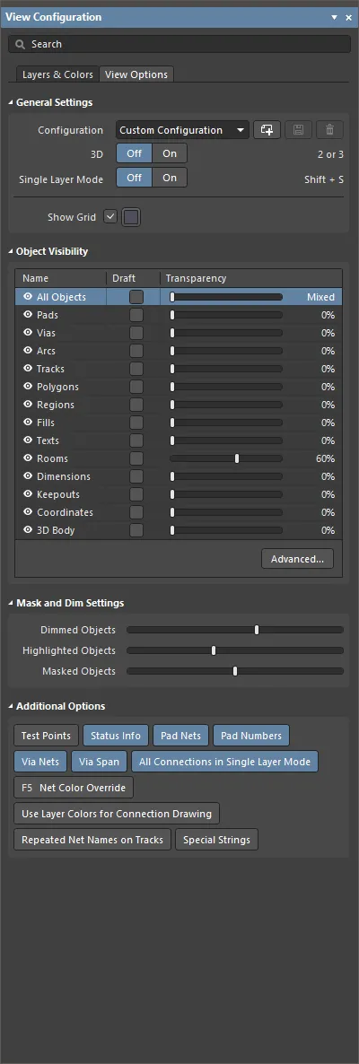
표시 관련 설정은 View Configuration 패널에서 구성합니다.
패널에 접근하는 표준 방법(설계 공간 오른쪽 하단의 Panels 버튼 또는 View » Panels 메뉴) 외에도, View Configuration 패널은 L 또는 Ctrl+D 바로가기 키를 사용해(각각 Layers & Colors 또는 View Options 탭이 표시된 상태로 패널을 열기) 접근할 수 있으며, 설계 공간 왼쪽 하단의 Layer Sets 컨트롤에서 색상 스와치를 클릭( )하여 접근할 수도 있습니다.
패널 내용은 두 개의 탭으로 나뉩니다. 패널 상단의 탭을 클릭하면 해당 탭에서 사용할 수 있는 옵션이 표시됩니다:
-
Layers and Colors 탭 – 사용 가능한 레이어의 가시성을 제어하고, mechanical layers를 추가/이름 변경/삭제하며, 패드 홀, 원점 마커, DRC 오류와 같은 특수 시스템 표시 기능의 색상과 가시성을 구성하는 옵션을 포함합니다.
-
View Options 탭 – 레이어 색상/가시성 구성(Configuration)을 선택, 저장 또는 로드하고, 객체 유형의 가시성을 구성하며, 마스킹 및 디밍 수준을 제어하고, 기타 표시 관련 옵션을 구성하는 옵션을 포함합니다.
사용 가능한 옵션은 현재 Layout Mode(2D 또는 3D)에 따라 달라집니다.
3D Layout 모드에서는
View Configuration 패널에서
Section View 탭도 사용할 수 있습니다. 이 탭을 사용해 PCB의 단면(섹션) 뷰를 구성할 수 있습니다 –
learn more.
레이어 가시성 구성
각 레이어는 View Configuration 패널의 Layers & Colors 탭에 있는 Layers 영역에서 표시하거나 숨길 수 있습니다. 가시성 아이콘( )을 클릭해 가시성을 켜고 끌 수 있습니다.

가시성 아이콘을 사용해 레이어 가시성 관리
해당되는 경우 각 그룹에도 가시성 아이콘이 포함됩니다. 예를 들어 위 이미지에서:
-
문자열 Component Layer Pairs (C) 왼쪽의 가시성 아이콘은 all 컴포넌트 레이어의 가시성을 켜고 끕니다.
-
문자열 Top 왼쪽의 가시성 아이콘은 all top side 컴포넌트 레이어의 가시성을 전환합니다. Bottom 측면(side) 레이어도 같은 방식으로 표시/숨김할 수 있습니다.
Controlling Layer Visibility from the Keyboard
복잡한 PCB 설계에서는 설계 과정 중 레이어를 자주 켜고 끄게 됩니다. 이를 돕기 위해, 다음과 같은 방식으로 키 입력을 사용해 레이어 가시성을 변경할 수 있습니다:
-
L 바로가기 키를 눌러 View Configuration 패널의 Layers & Colors 탭을 표시/활성화합니다. 패널의 제목 표시줄이 색상으로 표시되어, 소프트웨어에서 활성 요소임을 나타냅니다.
-
일부 레이어 및 레이어 세트 오른쪽에는 예를 들어 Component Layer Pairs (C), [1] Top (T)처럼 둥근 괄호 안에 문자와 숫자가 표시되어 있습니다. 이 둥근 괄호 안의 문자/숫자는 키보드 바로가기 키입니다. 예를 들어 L 바로가기를 눌러 패널을 활성화한 다음, T 바로가기를 눌러 Top 신호 레이어의 가시성을 전환할 수 있습니다.
-
레이어 세트에 접근한 상태라면, Spacebar을 눌러 해당 세트의 모든 레이어 가시성을 전환할 수 있습니다.
-
레이어에 접근한 상태라면, 가시성이 즉시 전환되며 이후 Spacebar을 사용해 다시 전환할 수 있습니다.
-
Up 또는 Down 화살표 키를 눌러 목록에서 위/아래로 이동할 수 있습니다. 예를 들어 특정 mechanical layer 또는 컴포넌트 레이어 쌍에 접근한 다음, Spacebar을 사용해 해당 레이어/레이어 쌍의 가시성을 전환할 수 있습니다.
-
대괄호 안의 숫자는 레이어 스택에서 해당 Signal 또는 Plane 레이어가 몇 번째 물리적 구리 레이어인지 나타냅니다. 문자열 [6] Bottom (B)를 예로 들면, [6]은 이것이 레이어 스택의 6번째 구리 레이어임을 의미하고, Bottom는 Layer Stack Manager에서 이 레이어에 사용자가 지정한 이름이며, (B)는 해당 레이어의 가시성을 전환하는 바로가기 키입니다.
-
Signal 및 Plane 레이어의 바로가기 키는 키보드에서 사용 가능한 마지막 숫자 키인 (9)에서 끝납니다.
Layer Sets
Layer Set 은 표시(가시) 레이어들의 이름이 지정된 집합입니다. 기존 Layer Set을 선택하려면 View Configuration 패널의 Layers & Colors 탭에 있는 Layers 영역의 Layers Sets 드롭다운을 사용합니다. 선택하면 해당 Layer Set에서 활성화된 레이어만 보이도록 표시가 업데이트됩니다. 사용자가 정의한 Layer Set은 원하는 만큼 만들 수 있으며, 현재 선택된 Layer Set도 편집할 수 있습니다.
-
새 사용자 정의 Layer Set을 만들려면 Layers 영역에서 필요한 대로 레이어 가시성을 설정한 다음
 버튼을 클릭합니다. 세트는 드롭다운에 My Layers로 표시됩니다. 이후 추가되는 각 Layer Set에는 번호가 매겨집니다.
-
기존 사용자 정의 Layer Set에서 활성화 레이어 구성을 변경하려면 Layers Sets 드롭다운에서 해당 세트를 선택하고 필요한 대로 레이어 가시성을 구성한 다음
 버튼을 클릭하여 Layer Set에 변경 사항을 저장합니다.
-
기존 사용자 정의 Layer Set의 이름을 바꾸려면 Layers Sets 드롭다운에서 선택한 뒤 Layer Sets 필드에 원하는 이름을 입력합니다. Layer Set 이름 변경은 저장 동작이 필요 없으며, 새 이름은 자동으로 저장됩니다.
-
기존 사용자 정의 Layer Set을 삭제하려면 Layers Sets 드롭다운에서 선택하고
 버튼을 클릭합니다.
-
PCB Layer Set File
(*.layerset) 에서 원하는 Layer Set을 가져오거나, 원하는 Layer Set을 PCB Layer Set File로 내보내려면 각각 Import 및 Export 버튼을 사용합니다.
다음 방법으로 표시되는 Layer Set을 전환할 수 있습니다:
-
Layer Set View Configuration 패널의 드롭다운
-
Design » Manage Layer Sets 하위 메뉴
-
Layer Set 컨트롤 - 디자인 공간 하단의 레이어 탭 왼쪽에 있는 버튼의 LS 부분을 클릭하여 접근(
 ).
).
System Colors
System Colors 영역에서는 목록에 있는 항목들에 대해 PCB에서 사용되는 색상을 구성할 수 있습니다. 색상과 가시성은 일반적인 방법으로 구성합니다.
Layer Tabs
View Configuration 패널에서 현재 표시로 설정된 각 레이어에 해당하는 탭은 디자인 공간의 하단 가장자리를 따라 배치됩니다.

이 탭을 통해 활성 레이어(객체를 배치할 레이어)를 전환할 수 있으며, 현재 표시 중인 레이어와 활성 레이어(강조 표시된 탭)가 무엇인지 시각적으로 알려줍니다. 한 번에 표시할 수 있는 레이어 탭 수보다 많으면 화살표  를 사용해 탭을 스크롤합니다.
레이어 색상은 레이어 탭의 왼쪽에 표시되며, 레이어 색상을 더블클릭하면 Choose Color 대화상자가 열립니다.
레이어 이름을 더블클릭하면 Edit Layer 대화상자가 열리며, 여기서 레이어 이름(및 internal plane layer의 경우 넷 이름)을 편집할 수 있습니다.

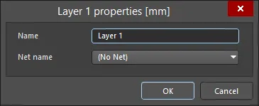
Edit Layer 대화상자
Single-Layer Mode
Single-Layer 2D Display Mode
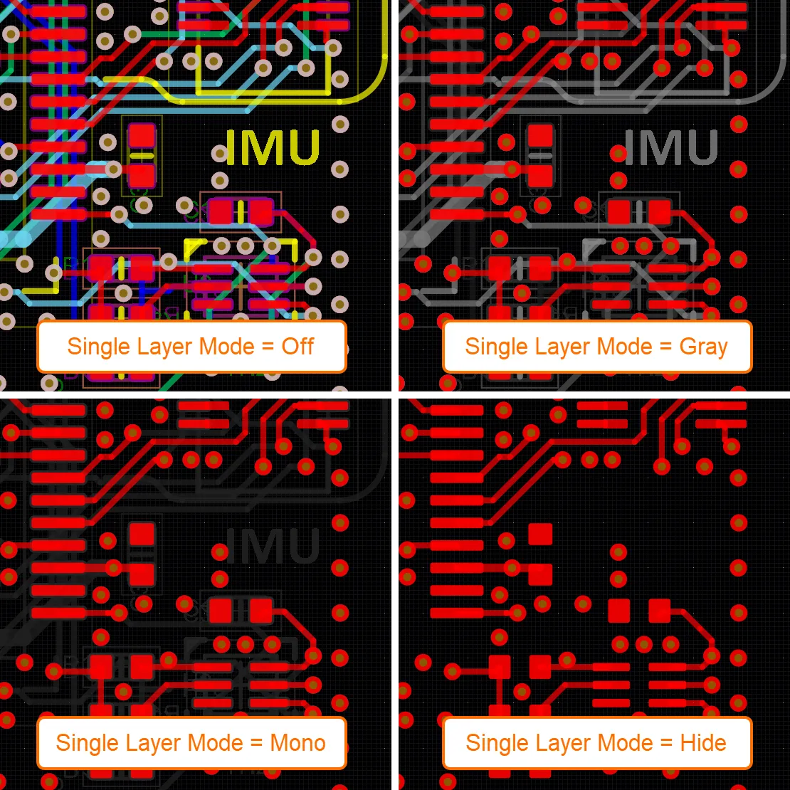
Board Insight에 통합된 Single-Layer 모드 기능은 Preferences 대화상자의 PCB Editor - Board Insight Display 페이지에서 구성합니다. Single Layer 모드는 현재 레이어의 내용은 표시하고, 다른 모든 레이어의 내용은 숨기거나 흐리게 표시합니다. 다른 모든 레이어의 모든 객체를 숨겨 현재 레이어 내용만 표시하는 것 외에도, Single-Layer 모드에는 그레이스케일 및 모노크롬 표시 모드가 있습니다. 다른 레이어의 모든 색상을 그레이스케일 또는 모노크롬으로 변환하면, 관심 레이어에 집중하는 데 방해받지 않으면서도 설계 내 다른 객체 위치에 대한 공간적 관계 정보는 유지할 수 있습니다. 전체 표시와 활성화된 각 단일 레이어 모드 사이를 순환하려면 Shift+S 바로가기를 누르십시오. Shift+S를 누를 때마다 소프트웨어는 다음으로 활성화된 모드로 이동하며, 최종적으로 전체 표시 모드로 돌아옵니다. 단일 레이어 모드는 Preferences 대화상자의 PCB Editor - Board Insight Display 페이지에서 활성화합니다. Shift+S를 눌렀을 때 포함하고 싶지 않은 모드는 비활성화(체크 해제)하십시오. 이 설정은 이 Altium Designer 설치본의 모든 설계에 적용됩니다.
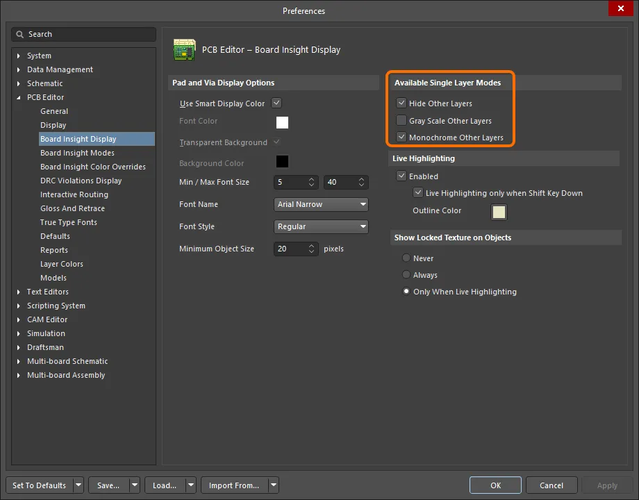
사용 가능한 단일 레이어 모드는 다음과 같습니다:
-
Hide Other Layers - 다른 모든 레이어를 숨김; 활성(현재) 레이어의 내용만 표시.
-
Gray Scale Other Layers - 다른 모든 레이어를 현재 레이어 색상에서 파생된 회색 음영으로 표시; 활성 레이어는 표준 색상으로 표시.
-
Monochrome Other Layers - 다른 모든 레이어를 동일한 회색 음영으로 표시; 활성 레이어는 표준 색상으로 표시.
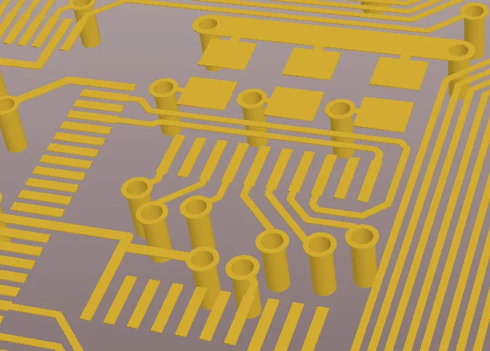
아래 이미지는 일반적인 멀티 레이어 표시와 3가지 단일 레이어 표시 모드를 보여줍니다.
현재 선택된 단일 레이어 모드는 View Configuration 패널의 View Options 탭에 있는 General Settings 영역에 표시됩니다. 모드 링크(On 버튼 옆)를 클릭하면 Preferences 대화상자의 PCB Editor - Board Insight Display 페이지로 이동하며, 여기서 사용 가능한 단일 레이어 모드를 필요에 맞게 구성할 수 있습니다.
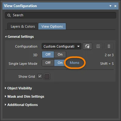
Gray 또는 Mono Single Layer 모드에서 다른 레이어의 밝기를 제어하려면 View Configuration 패널의 View Options 탭에 있는 Mask and Dim Settings 영역의 Masked Objects 슬라이더를 사용합니다.
Single-Layer 3D Display Mode
보드가 3D Layout Mode로 표시될 때도 단일 레이어 모드를 사용할 수 있습니다. 특정 레이어의 라우팅 품질이나 전원 플레인 레이어의 품질을 검사하는 등의 작업에 활용하십시오. 단일 레이어 모드에서는 Ctrl+Shift+Wheel Roll 바로가기를 사용해 레이어를 순차적으로 전환할 수 있습니다.
Single Layer Mode 표시에서 레이어를 항상 표시하기
Single Layer Mode 표시에 레이어를 포함하려면 View Configuration 패널의 Layers & Colors 탭에서 원하는 레이어에 연결된 눈(eye) 아이콘에 대해 Ctrl+Click을 수행하여 해당 레이어를 Single Layer Mode 표시로 추가합니다. 그러면 해당 레이어가 Single Layer Mode에서 항상 표시됨을 나타내기 위해 눈 아이콘 뒤에 사각형이 나타납니다( ).
).
보드를 바닥면에서 보기
보드를 바닥면에서 보려면(즉, 보드를 뒤집으려면) View Configuration 패널의 Layers & Colors 탭에 있는 Layers 영역에서 View From Bottom Side 옵션을 활성화하고, 메인 메뉴에서 View » Flip Board 명령을 선택하거나 Ctrl+F 키보드 바로가기를 사용합니다.
뒤집힌 보드/컴포넌트에 대해서도 모든 동작과 편집 명령이 지원됩니다. 좌표 공간은 논리적으로 동일하게 유지되며, 즉 디자인 공간 원점이 좌하단에서 우하단으로 이동합니다. 현재 그리드 위치는 마우스를 정상적인 좌→우가 아니라 우→좌로 움직일 때 X(수평) 방향으로 증가합니다. 뷰가 뒤집힌 상태에서 생성된 모든 출력은 올바른 ‘위에서 본(viewed-from-top)’ 좌표 정보를 유지합니다.
보드/컴포넌트를 뒤집으면 레이어 그리기 순서도 논리적인 쌍 교환(pair-swapping) 방식으로 변경됩니다. 즉, 현재 레이어 그리기 순서에서 Top Overlay 는 Bottom Overlay와, Top Layer 는 Bottom Layer와, Mid-Layer 1 는 Mid-Layer 30와, Internal Plane 1 는 Internal Plane 16와 서로 위치를 바꾸는 식으로 계속됩니다. 기계(Mechanical) 레이어의 그리기 순서는 변경되지 않습니다.
객체 가시성 제어
레이어를 켜고 끄는 방식으로 디자인 공간의 객체 표시를 제어하는 것 외에도, 객체 유형에 따라 객체의 가시성과 투명도를 제어하는 방법이 있습니다. 2D Layout 모드에서는 View Configuration 패널의 View Options 탭에 있는 Object Visibility 영역에서 제공하는 옵션을 사용하여 유형별 객체 가시성과 투명도를 구성합니다.

패널의 View Options 탭에 있는 Object Visibility 섹션
-
– 해당 가시성 아이콘을 클릭하여 특정 객체 유형의 가시성을 제어합니다. All Objects 가시성 아이콘을 클릭해 모든 객체의 가시성을 토글한 다음, 특정 객체 유형의 가시성을 활성화하십시오.
-
Name – 시각적으로 조정할 수 있는 모든 객체를 나열합니다.
-
Draft – 활성화하면 해당 객체 유형을 윤곽선으로 표시합니다.
-
Transparency – 슬라이더 바를 사용하거나 값을 클릭한 뒤 0~100 사이의 원하는 백분율을 수동으로 입력하여 해당 객체 유형의 투명도를 조정합니다(0%는 완전 표시(불투명/솔리드), 100%는 완전 투명(보이지 않음)). 객체를 투명하게 설정하면 예를 들어 트랙 세그먼트 끝이 패드와 만나는 지점처럼, 한 객체가 다른 객체를 덮는 경우를 확인할 수 있습니다.
-
Advanced – 클릭하면 Object Visibility 대화상자가 열리며, 여기서 서로 다른 레이어에 걸쳐 특정 객체에 대한 공통 투명도 수준을 설정하고, 특정 레이어에서 서로 다른 객체에 대해 서로 다른 투명도를 설정할 수 있습니다.
이 패널의 General Settings 영역에서 Custom Configuration을 생성하여 선호하는 가시성 설정을 쉽게 복원할 수 있습니다.
Mask and Dim Settings
단순한 PCB 설계에서도 매우 많은 객체가 존재할 수 있으므로, 이러한 객체 표시를 관리할 수 있도록 PCB 편집기에는 관심 없는 객체를 페이드(fade) 처리하는 기능이 있습니다. 예를 들어 PCB 패널의 Nets 모드에서 네트를 클릭하고, 패널 드롭다운이 Dim 또는 Mask로 설정되어 있으면 해당 네트에 속하지 않는 모든 객체가 페이드 처리됩니다. 이를 통해 네트 또는 네트 클래스, 컴포넌트 클래스, 특정 설계 규칙이 대상으로 하는 객체 등 특정 설계 요소에 더 쉽게 집중할 수 있습니다. 마스킹과 디밍 수준은 View Configuration 패널의 View Options 탭에 있는 Mask and Dim Settings 영역의 슬라이더로 설정합니다.

View Configuration 패널의 View Options 탭에 있는 Mask and Dim Settings 영역
구성(Configurations) 관리
구성(configuration)은 레이어 색상과 레이어 가시성 설정을 미리 묶어둔 정의입니다. View Configuration 패널의 View Options 탭에 있는 General Settings 영역의 Configuration 드롭다운에서 기존 구성을 선택하거나, 드롭다운 옆 버튼을 사용해 구성을 생성/저장/삭제할 수 있습니다. 사용자 정의 구성은 현재/마지막으로 사용한 2D 및 3D 표시 설정을 모두 저장합니다.
-
– 클릭하여 새 사용자 정의 구성을 만든 다음 새 이름을 입력하고 버튼을 클릭합니다.
-
– 새 사용자 정의 구성을 만들 때 또는 현재 선택된 사용자 정의 구성을 편집한 경우 클릭하여 저장합니다.
-
– 현재 선택된 사용자 정의 구성을 삭제하려면 클릭합니다.
-
생성 및 저장된 사용자 정의 구성은 자동으로 로드되며 Configuration 필드의 드롭다운 목록에서 선택할 수 있습니다.
-
Configuration 필드의 드롭다운에서 Load View Configuration 옵션을 사용하면, 현재 Altium Designer 설치의 표준 위치가 아닌 곳에 저장된 구성 파일을 로드할 수 있습니다. 사용자 정의 구성은 Complex Configuration(파일 확장자
.config_complex)으로 저장되므로, 사용자 정의 구성을 로드할 때 Open 대화상자에서 File Type 드롭다운을 변경해야 할 수도 있습니다.
추가 옵션
View Configuration 패널의 View Options 탭에 있는 Additional Options 영역에는 특정 요소의 뷰를 제어하는 추가 옵션이 있습니다.

View Configuration 패널의 View Options 탭에 있는 Additional Options 섹션
-
Test Points – 이 옵션을 활성화하면 테스트포인트로 구성된 패드와 비아에 추가 정보가 표시됩니다. 패드 또는 비아는 Properties 패널의 해당 모드에서 Fabrication 및/또는 Assembly Testpoint 옵션을 활성화하여 테스트포인트로 구성할 수 있습니다. 테스트포인트는 패드/비아에 문자열
<Layer> Fab Testpoint 또는 <Layer> Assy Testpoint를 추가하여 표시됩니다.
-
Status Info – 이 옵션을 활성화하면 설계 공간에서 객체 위에 마우스를 올렸을 때 좌표 위치, 레이어 등의 요약 정보가 Status Bar에 표시됩니다.
-
Pad Nets – 이 옵션을 활성화하면 패드에 연결된 네트 이름이 표시됩니다. 네트 이름은 충분히 확대(zoom in)했을 때만 보입니다.
-
Pad Numbers – 이 옵션을 활성화하면 패드 번호가 표시됩니다. 패드 번호는 충분히 확대했을 때만 보입니다.
-
Via Nets – 이 옵션을 활성화하면 비아에 해당 네트 이름이 표시됩니다. 네트 이름은 충분히 확대했을 때만 보입니다.
-
Via Span – 이 옵션을 활성화하면 비아가 허용되는 스팬(span) 길이가 표시됩니다. 이후 배치된 비아의 속성(지름, 홀 크기 등)은 설계 규칙 또는 수동으로 정의됩니다. 네트 이름은 충분히 확대했을 때만 보입니다. 비아 스팬에 포함된 레이어 번호는 모든 비아 유형 내부에 표시할 수 있습니다.
-
All Connections in Single Layer Mode – 이 옵션을 활성화하면 Single Layer Mode에서 항상 모든 연결선(connection line)이 표시됩니다. 이 옵션이 비활성화되어 있으면, 현재 레이어에서 시작하거나 끝나지 않는 연결선은 관련이 없다고 가정하여 Single Layer Mode로 전환할 때 함께 숨겨집니다.
-
Net Color Override – 각 네트에는 색상을 할당할 수 있습니다. 색상을 설정하려면 PCB 패널의 Nets 모드에서 해당 네트 이름을 더블클릭하면 Edit Net dialog 가 열립니다. 색상은 해당 네트의 연결선에 자동 적용되며, 이 옵션을 활성화하면 라우팅에도 적용할 수 있습니다. 라우팅에 대한 색상 적용은 Preferences 대화상자의 PCB Editor – Board Insight Color Overrides page 의 현재 설정을 따르며, 여기서 Pattern 옵션으로 색상 적용 방식을 정의하고 Zoom Behavior로 색상이 적용되는 시점을 정의합니다. F5 단축키를 눌러 Net Color Override 옵션을 켜고 끌 수 있습니다.
-
Use Layer Colors for Connection Drawing – 이 옵션을 활성화하면 연결선이 지나가는 시작/종료 레이어의 색상을 사용해 연결선이 표시됩니다. 연결선은 시작/종료 객체에서는 순수 레이어 색상으로 표시되고, 연결선 길이를 따라 두 레이어 색상 사이로 점진적으로 변합니다(morphing). 이 기능은 멀티 레이어 보드를 라우팅할 때 유용하며, 라우팅 중인 연결이 도달해야 하는 대상 레이어를 알려줍니다. 색상 변환은 한 레이어에서 다른 레이어로 이동하는 연결에만 적용됩니다. 연결이 같은 레이어에서 시작하고 끝나면 할당된 네트 색상을 유지합니다.
-
Repeated Net Names on Tracks – 트랙에 반복되는 네트 이름을 표시하도록 활성화합니다.
-
Special Strings – 이 옵션이 활성화되면, 변환된 Special Strings로부터 생성된 배치된 String은 변환되지 않은 Special String 이름이 위에 겹쳐(라벨로) 표시됩니다. 라벨 오버레이를 보려면 String을 확대하세요.


 AI로 번역됨