
간단한 배치
PCB 설계 작업 공간에서는 부품을 이동, 회전, 뒤집기(Flip)할 수 있습니다. 이를 위해 작업 공간에서 해당 부품을 클릭하여 선택합니다. 선택된 부품은 아래 이미지와 같이 현재 선택 색상으로 하이라이트 표시됩니다.
 한 번 클릭하여 부품을 선택합니다.
-
클릭한 채로 드래그하여 선택된 부품을 이동합니다. 커서는 부품 기준점(reference point)으로 이동하거나, Smart Component Snap 옵션이 PCB Editor - General page 의 Preferences dialog에서 활성화되어 있는 경우 가장 가까운 패드 중심으로 이동합니다. 이동 중 Alt 키를 누르면, 최초 이동 방향에 따라 수평 또는 수직 축으로만 이동하도록 방향이 제한됩니다.
-
부품이 커서에 붙어 이동 중일 때 Spacebar를 눌러 회전합니다(Shift+Spacebar는 반대 방향으로 회전). 기본 회전 각도(step)는 90도입니다. 이 설정을 변경하려면 Preferences dialog의 PCB Editor - General page에서 Rotation Step 값을 사용합니다.
-
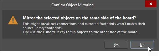
부품이 커서에 붙어 이동 중일 때 L 키를 누르면 보드의 반대면으로 뒤집습니다(Flip).
-
Delete를 눌러 선택된 부품을 PCB에서 제거합니다.
 ).
).연결선(connection line)은 부품 배치 중 서로 연결된 부품을 찾고 방향을 잡는 데 매우 유용합니다. 부품을 이동하면 연결선은 동적으로 최적화되어, 각 연결선이 동일한 넷 이름을 가진 다른 객체까지의 최단 경로를 따르도록 합니다.

연결선을 사용하여 부품의 위치를 찾고 방향을 맞추는 데 활용합니다.
시각적 혼잡을 줄이기 위해, 부품을 이동하는 동안에는 해당 부품에 연결된 연결선을 제외한 모든 연결선이 숨겨집니다. N 키를 눌러 넷 라인 연결 모드를 순환 전환합니다. 다음 모드가 지원됩니다:
- Pad to Pad - 이동 중, 이동 중인 부품의 패드와 보드에서 동일 넷의 가장 가까운 패드 사이에 연결선이 표시됩니다.
- Breaks - 이동 중, 이동 중인 부품의 패드와 보드에서 동일 넷의 트랙 브레이크(track breaks) 사이에 연결선이 표시됩니다.
- Hidden - 연결선이 숨겨집니다.
현재 넷 라인 연결 모드는 Status Bar 및 Heads Up Display에 표시됩니다.
 AI로 번역됨