
Проектирование жестко-гибкой печатной платы
Что такое Rigid-Flex?
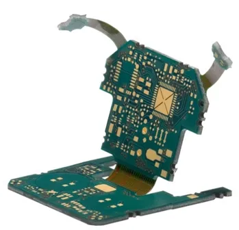
Как следует из названия, гибкая печатная схема — это рисунок проводников, нанесённый на гибкую изоляционную плёнку. Rigid-flex — это название печатной платы, которая представляет собой комбинацию как гибкой(их) схемы(схем), так и жёсткой(их) схемы(схем), как показано на изображении.
Технология гибких печатных схем изначально была разработана для космической программы, чтобы экономить место и массу. Сегодня она популярна, поскольку не только экономит место и вес — что делает её идеальной для портативных устройств, таких как мобильные телефоны и планшеты, — но также может снижать сложность компоновки/упаковки, повышать надёжность изделия и уменьшать стоимость.
Гибкие схемы обычно делят на два класса применения: static статические гибкие схемы, и dynamic динамические гибкие схемы. Статические гибкие схемы (также называемые use A), — это те, которые подвергаются минимальному изгибу во время сборки и эксплуатации. Динамические гибкие схемы (также называемые use B), — это те, которые рассчитаны на частые изгибы, например, в узле головки дискового накопителя, в печатающей головке или как часть шарнира экрана ноутбука. Это различие важно, поскольку оно влияет и на выбор материалов, и на методику построения. Существует ряд конфигураций слоёв (stackup), которые могут изготавливаться как rigid-flex, и каждая из них имеет свои электрические, механические и стоимостные преимущества.
Механическое проектирование Rigid-Flex
Проектирование гибкой или rigid-flex схемы во многом является электромеханическим процессом. Проектирование любой печатной платы — это трёхмерный процесс, но для flex или rigid-flex трёхмерные требования значительно важнее. Почему? Потому что rigid-flex плата может крепиться к нескольким поверхностям внутри корпуса изделия, а процесс крепления и складывания часто происходит во время сборки. Получение работоспособной электромеханической конструкции требует тесного и постоянного взаимодействия между командами механиков и электронщиков. Традиционный способ проверить, помещается ли сложенная плата в корпус, — сделать механический макет, известный как «бумажная кукла» (paper doll cut out). По своей природе этот подход затрудняет достижение требуемой точности и реалистичности.
 Плата с двумя жёсткими областями, соединёнными гибкой областью, в редакторе ECAD PCB и в MCAD.
Altium помогает решать эту задачу с помощью CoDesigner — продвинутой технологии интерфейса «механика‑электроника». CoDesigner позволяет инженерам передавать форму платы и изменения компонентов туда и обратно между средами проектирования ECAD и MCAD непосредственно из ПО ECAD и MCAD.
-
Обзор технологии Altium MCAD CoDesigner
-
Техническая справка: узнайте больше о ECAD-MCAD CoDesign
-
Узнайте больше о передаче rigid-flex проекта в MCAD
Проектирование Rigid-Flex PCB
Печатная плата проектируется как набор слоёв, уложенных друг на друга. Для традиционной жёсткой печатной платы контур платы задаёт плату в плоскости X‑Y, а стек слоёв задаёт плату по оси Z. Контур X‑Y задаётся в основном окне редактирования PCB, а слои настраиваются в Layer Stack Manager. В rigid-flex PCB в готовой плате есть более одной зоны или области (Region), и каждая из этих областей может использовать свой набор слоёв.
Чтобы спроектировать rigid-flex плату, необходимо:
-
Включить требуемый режим Rigid-Flex (Layer Stack Manager, Tools » Features » Rigid-Flex, или Tools » Features » Rigid-Flex (Advanced) command)
-
Определить Substack, необходимый для каждой области (Region) платы, и настроить, как эти Substack выравниваются относительно друг друга по оси Z.
-
Определить форму каждой жёсткой и гибкой области (Region) в плоскости X‑Y и назначить каждой области правильный Substack.
Включение проектирования Rigid-Flex
Чтобы поддержать сложные структуры, присутствующие в современной rigid-flex печатной плате, редактор по оси Z — Layer Stack Manager — предоставляет разные режимы отображения для редактирования структуры платы. Выберите команду Design » Layer Stack Manager, чтобы открыть Layer Stack Manager, где можно включить нужный режим rigid-flex и создать/выровнять Substack, необходимые в вашем rigid-flex проекте.
При открытии Layer Stack Manager будет показан текущий stackup слоёв платы. Для новой PCB это будет простая двухслойная плата. Чтобы включить функции, необходимые для проектирования rigid-flex платы, откройте подменю Tools » Features или нажмите кнопку Features ( ![]() ), чтобы выбрать либо стандартный режим Rigid-Flex (также называемый RF1), либо режим Rigid-Flex (Advanced) (также называемый RF2).
), чтобы выбрать либо стандартный режим Rigid-Flex (также называемый RF1), либо режим Rigid-Flex (Advanced) (также называемый RF2).
 Выберите команду, чтобы включить требуемый режим rigid-flex.
Выбор стандартного или расширенного режима Rigid-Flex
В ПО для проектирования печатных плат Altium доступны два режима проектирования rigid-flex. Исходный, или стандартный режим, называемый Rigid-Flex (или rigid-flex 1), поддерживает rigid-flex проекты, включающие: одно или несколько определений stackup для жёстких и гибких участков. Чтобы использовать стандартный режим rigid-flex, вы должны иметь возможность определить плату целиком как одну плоскую форму при виде сверху, без перекрывающихся областей. Именно так работает режим rigid-flex 1: задаётся единый общий контур платы, затем размещаются линии разделения (split lines), которые делят этот контур на различные жёсткие и гибкие области. После этого каждой области можно назначить стек слоёв.
Узнайте больше о проектировании rigid-flex платы в стандартном режиме.
Если в вашем проекте есть более сложные требования к rigid-flex, например перекрывающиеся гибкие области, тогда нужен режим Advanced Rigid-Flex (также известный как rigid-flex 2.0). Помимо перекрывающихся гибких областей, расширенный режим также добавляет: визуальное определение субстеков в плоскости Z, независимое определение каждой жёсткой и гибкой области платы, сгибы на вложенных вырезах, разделения произвольной формы, возможность задавать структуры типа «книжный переплёт», возможность добавлять coverlay на гибкую область и поддержку проектов только с гибкими участками (flex-only).
Узнайте больше о проектировании rigid-flex платы в расширенном режиме.
Переход со стандартного режима на расширенный
Переход со стандартного режима на расширенный выполняется в Layer Stack Manager, как показано на изображении выше. Когда вы выбираете опцию Rigid-Flex (Advanced) в меню Tools » Features, ПО автоматически преобразует единый контур платы в несколько объектов областей платы (board region) и назначает стеки слоёв соответствующим образом. Видео ниже демонстрирует процесс.
Обзор перехода со стандартного режима rigid-flex на расширенный режим.
Работа с областями платы (Board Regions)
Board Region — термин, используемый для описания каждой определённой пользователем области платы, которой нужно назначить уникальный стек слоёв — стандартное требование для rigid-flex PCB. На изображении ниже контур платы разделён на три отдельные области платы (Board Regions): верхнюю круглую область, тонкую центральную полоску и нижнюю круглую область.
, каждая показывает имя области и назначенный ей стек слоёв.")
Rigid-flex плата в режиме Board Planning Mode; обратите внимание, что контур платы разделён на три отдельные области платы (Board Regions), каждая показывает имя области и назначенный ей стек слоёв.
При создании новой платы по умолчанию она имеет одну область платы (Board Region). Если для проекта требуется несколько областей, то вы можете либо:
- разрезать одну область платы (Board Region) на несколько областей (стандартный режим Rigid-Flex или расширенный режим Rigid-Flex), либо
- разместить несколько областей платы (Board Regions), чтобы собрать общий контур (расширенный режим Rigid-Flex).
Области платы (Board Regions) задаются и редактируются в режиме Board Planning Mode (меню View).
Работа с линиями сгиба
Линии сгиба задаются и редактируются в режиме планирования платы (меню View).
Свойства линии сгиба
Линии сгиба имеют следующие взаимосвязанные свойства:
- Bend Angle (a) — угол, на который должна изгибаться поверхность гибкой (Flex) области.
-
Radius (
r) — расстояние от поверхности сгиба до точки, в которой расположен центр изгиба. -
Width (
w) — ширина участка поверхности, который будет изгибаться для заданных Radius и Bend Angle.
Связь между Bend Angle, Radius и width можно выразить как:
-
w = a/360 * 2*Pi*r -
или словами,
width = Fraction of the circumference being bent * Circumference

Просмотр областей стека слоёв и линий сгиба
В режиме PCB panel’s Layer Stack Regions три основные области панели изменяются и отражают следующее (сверху вниз):
- Имена доступных Layer Stacks.
- Stackup Regions, определённые на плате, или назначенные выбранному стеку слоёв (Layer Stack).
- Список Bending Lines в выбранной области стека (Stackup Region)
При использовании режима Layer Stack Regions панели PCB переключитесь на вид режима планирования платы через меню View » Board Planning Mode или используйте сочетание клавиш 1.
, которым назначаются конкретные варианты построения стека слоёв (Layer Stacks). Области сгиба (Bending Lines) задаются в гибких областях платы.")
Плата может быть разделена на отдельные области (Stackup Regions), которым назначаются конкретные варианты построения стека слоёв (Layer Stacks). Области сгиба (Bending Lines) задаются в гибких областях платы.
Когда в области Layer Stacks панели PCB выбирается имя конкретного стека слоёв, применяется фильтрация с использованием Layer Stack в качестве области действия фильтра. Поэтому любые области платы, назначенные этому стеку, будут перечислены в области Stackup Regions панели. В свою очередь, любые линии сгиба, определённые в выбранной области Stackup Region, будут перечислены в списке области Bending Lines.
Двойной щелчок по области Stackup Region в списке (или двойной щелчок по самой области платы в рабочем пространстве) открывает диалог Board Region dialog (стандартный режим Rigid-Flex) или режим Board Region панели Properties (расширенный режим Rigid-Flex). Используйте этот диалог/панель, чтобы переименовать область, назначить её стеку слоёв или заблокировать её 3D-свойства.
Двойной щелчок по линии сгиба в списке области Bending Line панели открывает диалог Bending Line dialog , в котором свойства линии можно детально отредактировать.
Отображение и складывание Rigid-Flex-проекта в 3D
PCB-редактор включает мощный движок 3D-визуализации, позволяющий показывать высокореалистичное трёхмерное представление загруженной печатной платы. Этот движок также поддерживает Rigid-Flex-платы и, в сочетании с ползунком Fold State на панели PCB , позволяет конструктору просматривать Rigid-Flex-проект в плоском состоянии (без применения настроек линий сгиба), в полностью сложенном состоянии (применены все настройки линий сгиба) и в любом промежуточном положении.
Чтобы переключиться в режим 3D-отображения, нажмите клавишу быстрого доступа 3 (нажмите 2, чтобы вернуться в 2D или 1, чтобы вернуться в режим планирования платы). Плата будет показана в 3D. Если посадочные места компонентов содержат 3D-объекты корпуса, определяющие установленный компонент, они также будут отображены. На изображении ниже видно, что плата включает батарею и держатель батареи.
Чтобы применить все линии сгиба, переместите ползунок Fold State на панели PCB, когда она установлена в режим Layer Stack Regions, как показано на изображении ниже. Обратите внимание: сгибы применяются в порядке, заданном их номером последовательности. Линии сгиба могут иметь одинаковый номер последовательности; это просто означает, что эти сгибы будут выполняться одновременно при использовании ползунка Fold State. Плату также можно складывать/раскладывать, запуская команду View » 3D View Control » Fold/Unfold (или нажимая сочетание клавиш 5).
, чтобы применить все линии сгиба в порядке, определённом их значением последовательности (Fold Index).")
Используйте ползунок Fold State (или сочетание клавиш 5), чтобы применить все линии сгиба в порядке, определённом их значением последовательности (Fold Index).
Поддержка 3D Movie Maker для Rigid-Flex-проектов
Возможность складывать Rigid-Flex-проект также можно записать в виде 3D-видео. Это делается очень просто и не требует использования ключевых кадров во время последовательности складывания.
Подробное описание создания 3D-видео см. на странице Preparing a 3D PCB Video page. В качестве базового руководства:
- Переключите PCB-редактор в 3D-режим.
- Откройте панель PCB 3D Movie Editor и создайте новое видео, нажав кнопку New . Щёлкните по только что созданному видео в области Movie Title, затем задайте ему подходящее имя.
- Создайте начальный Key Frame, показывающий плату в разложенном состоянии.
- Переместите ползунок Fold State, чтобы показать Rigid-Flex-проект в сложенном состоянии, затем расположите сложенную плату нужным образом.
- Теперь создайте второй Key Frame для этого вида и задайте время. Определите, сколько должно занимать складывание Rigid-Flex-проекта (параметр Duration); обычно это несколько секунд.
-
Чтобы проверить, что видео корректно фиксирует процесс складывания, нажмите кнопку воспроизведения (расположена в элементах управления плеером в нижней части панели).

- Чтобы сформировать файл фильма, добавьте PCB 3D Video Documentation Output в файл Output Job. Не забудьте настроить параметры формата видео в диалоге Video settings dialog.
- Щёлкните ссылку Generate Content в файле Output Job, чтобы создать файл фильма.
Видео ниже было создано с использованием этого процесса. В нём есть два ключевых кадра, описанных выше, плюс один дополнительный ключевой кадр, добавленный в конце, чтобы удерживать финальное положение в течение одной секунды.
.") Простое 3D-видео, созданное из трёх ключевых кадров; поведение складывания определяется значениями последовательности линий сгиба (Bending Line Sequence).
Простое 3D-видео, созданное из трёх ключевых кадров; поведение складывания определяется значениями последовательности линий сгиба (Bending Line Sequence).
► Узнать больше о Preparing a 3D PCB Video
Рекомендации по проектированию
Ниже приведено резюме ключевых аспектов, которые необходимо учитывать при проектировании Rigid-Flex-платы:
- Трассировка проводников — важен выбор типа углов для дорожек, проходящих через гибкую область; избегайте острых углов; используйте дугу, чтобы минимизировать напряжения.
- Форма и площадь площадок — используйте скругления (teardrops) с «кроличьими ушами» (анкерными выступами) для одностороннего флекса. Цель — захватить часть формы площадки покровным слоем (coverlayer).
- Сквозные отверстия — старайтесь избегать сквозных отверстий в зоне изгиба, особенно в динамических применениях.
- Покровный слой (coverlayer) — избегайте концентраторов напряжений (оголения входящей дорожки); уменьшите окно в coverlayer до 250 мкм.
- Полигоны/плоскости — по возможности выполняйте сеткой (crosshatched).
- Смещение длин слоёв — чтобы избежать коробления слоёв при изгибе (эффект «переплёта»), смещайте длины слоёв примерно на 1,5 толщины слоя.
- Сервисная петля — сделайте гибкую область немного длиннее, чтобы облегчить сборку/разборку и учесть размерные вариации изделия (дополнительная длина называется service loop).
- Экономия меди — учитывайте, как гибкая схема будет панелизироваться; возможно, лучше скорректировать проект, чтобы обеспечить наилучшее использование материала.
- Панелизация — ориентируйте гибкие области с учётом направления волокон материала (гнуть вдоль волокон).
- Сопротивление разрыву — скруглённые углы; просверленное отверстие в углу; отверстие в прорези; оставляйте металл в углах.
- Трассировка — на двухслойных платах смещайте дорожки, чтобы избежать эффекта «двутавра» (I-beaming), и расширяйте дорожки в зоне изгиба (это особенно важно для постоянных изгибов).
- Static Bend Ratio — задание соотношения радиуса изгиба к толщине схемы. В идеале для многослойных схем соотношение изгиба должно быть не менее 15:1. Для двусторонних схем минимальное соотношение должно быть не менее 10:1. Для однослойных схем минимальное соотношение также должно быть не менее 5:1. Для динамического применения ориентируйтесь на соотношение изгиба 20–40:1.
- Отожжённая прокатанная медь более пластична; гальванически осаждённая медь — не лучший выбор для гибких участков.
Требования к документации и чертежам
Типичные рекомендуемые требования к документации включают:
- Гибкая печатная плата (Flex PCB) должна изготавливаться по стандарту IPC-6013, класс (укажите ваше требование).
- Гибкая печатная плата (Flex PCB) должна соответствовать минимальному классу горючести V-0 (при необходимости).
- Гибкая печатная плата (Flex PCB) должна соответствовать RoHS (при необходимости).
- Жёсткий материал должен быть GFN по IPC-4101/24 (при использовании эпоксидного материала).
- Жёсткий материал должен быть GIN по IPC-4101/40 (при использовании полиимидного материала).
- Гибкий фольгированный материал (copper clad) должен соответствовать IPC 4204/11 (гибкий безадгезивный фольгированный диэлектрический материал).
- Материал покровного слоя (covercoat) должен соответствовать IPC 4203/1.
- Максимальная толщина платы не должна превышать (укажите ваше требование) и применяется после всех процессов ламинирования и металлизации. Измеряется по готовым металлизированным поверхностям.
- Толщина акрилового клея в жёсткой части панели не должна превышать 10% от общей конструкции. См. комментарии выше.
- Для упрощения производства можно использовать материал-«пакет» (pouch material), и он должен быть удалён с гибкой части платы перед отгрузкой.
- Толщина гибкой секции должна быть (укажите ваше требование). Не добавляйте это примечание, если данная толщина не критична.
- Минимальная толщина медной стенки металлизированных сквозных отверстий — (укажите ваше требование; рекомендуется среднее .001”) при минимальной ширине кольца (annular ring) (укажите ваше требование; рекомендуется 002).
- Нанести зелёную паяльную маску LPI (при необходимости) поверх открытой меди с обеих сторон только в жёстких секциях платы. Все открытые металлы будут (укажите требование к финишному покрытию здесь).
- Нанести шелкографию с обеих сторон платы (при необходимости) белой или жёлтой (наиболее распространено) непроводящей эпоксидной краской.
- Требования к маркировке и идентификации.
- Требования к электрическим испытаниям.
- Требования к упаковке и отгрузке.
- Требования по импедансу.
Дополнительные детали чертежа
- Таблица сверления с указанием готового диаметра отверстий, соответствующих допусков и признака металлизации/неметаллизации.
- Размерный чертёж, включая базовую(ые) поверхность(и) (datum), критические размеры, интерфейсы rigid-to-flex, место изгиба и маркеры направления.
- Детали панелизации, при необходимости.
- Детали конструкции и слоёв, с указанием материала для каждого слоя, толщин и толщины меди (copper weight).
Ссылки
Техническое инженерное руководство по гибким и гибко-жёстким схемам - Epec Engineering Technologies
Технология гибких схем - Joe Fjelstad
Руководство по проектированию гибких схем - Minco Products Inc
Ресурсы Minco Products по гибким платам
Сайт Machine Design:
- Основы проектирования гибких схем - Robert Repas
- Сохраняя гибкость - Mark Finstad, инженер по применению
 Локализовано с помощью ИИ