Работа с дорожками
Сегмент дорожки — это прямая линия заданной ширины. Дорожки используются для задания прямых линий в рабочем пространстве проектирования печатной платы. Дорожки размещаются на сигнальном слое, формируя электрические соединения, или трассировку, между площадками компонентов. Дорожки, размещенные на неэлектрическом слое, называются линиями (Lines) и используются как универсальные элементы черчения для создания контуров компонентов, поясняющей информации, границ keepout и т. п. Дорожки также используются в составных объектах проектирования, таких как размеры и координаты.

Объекты дорожек применяются для трассировки и для универсальных линий черчения. На изображении выше размещены четыре сегмента дорожек, и еще один находится в процессе размещения.
Хотя дорожки и линии фактически являются одним и тем же объектом, различие заключается в том, как ведет себя программа при их размещении — поэтому существуют разные команды. Когда выполняется команда размещения дорожки, например Interactive Routing, программа отслеживает место щелчка и автоматически принимает имя цепи (net) существующего объекта (например, площадки) под точкой щелчка. Также она отслеживает и соблюдает все применимые правила проектирования. Когда выполняется команда размещения линии (Place » Line), такое отслеживание не выполняется.
Дорожки доступны для размещения как в PCB Editor, так и в редакторе PCB Library. Независимо от того, какая команда используется (трассировка/дорожка или размещение линии), базовое поведение при размещении одинаково. После запуска команды курсор изменится на перекрестие, и вы перейдете в режим размещения дорожек. Размещение выполняется следующей последовательностью действий:
-
Щелкните или нажмите Enter, чтобы зафиксировать начальную точку первого сегмента дорожки. Если выполняется команда размещения типа трассировки и вы щелкнете, начиная размещение на существующем объекте, дорожка примет имя цепи этого объекта. Для трассировки ширина будет определяться применимым правилом проектирования Routing Width; это можно переопределить некоторыми интерактивными параметрами трассировки, которые подробнее описаны ниже.
-
Переместите курсор, чтобы задать сегмент дорожки, затем щелкните или нажмите Enter , чтобы зафиксировать конечную точку этого первого сегмента — она же является начальной точкой следующего соединенного сегмента.
-
Продолжайте позиционировать курсор, затем щелкайте или нажимайте Enter , чтобы зафиксировать серию вершин, определяющих последовательность соединенных сегментов дорожки.
-
Щелкните правой кнопкой мыши или нажмите Esc, чтобы завершить текущую серию соединенных сегментов дорожки.
Дополнительные действия, которые можно выполнять во время размещения, включают:
-
Нажмите клавишу * на цифровой клавиатуре, чтобы циклически переключаться между доступными сигнальными слоями. Либо используйте сочетание Shift+Ctrl+Wheel Roll для перемещения по слоям трассировки; каждый щелчок колесика мыши будет переходить на следующий (или предыдущий) доступный сигнальный слой.
-
Нажмите клавиши + и - на цифровой клавиатуре, чтобы циклически переключаться вперед и назад по всем слоям, которые в данный момент видимы в проекте.
При размещении сегментов дорожки доступны пять режимов углов, четыре из которых также имеют подрежимы направления угла. Во время размещения:
-
Нажмите Shift+Spacebar, чтобы циклически переключаться между доступными режимами углов.
-
Нажмите Spacebar, чтобы переключаться между двумя подрежимами направления угла.
-
Находясь в одном из режимов угла с дугой, удерживайте клавишу , или . для уменьшения или увеличения дуги. Удерживайте клавишу Shift при нажатиях, чтобы ускорить изменение размера дуги.
-
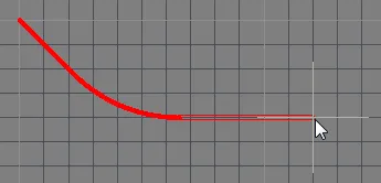
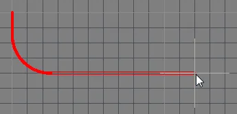
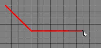
Нажмите сочетание клавиш 1, чтобы переключаться между размещением одного сегмента на щелчок (показано на первых пяти изображениях ниже) и двух сегментов на щелчок (показано на последнем изображении ниже). В первом режиме полый сегмент дорожки называется сегментом предварительного просмотра (look-ahead).
-
Нажмите клавишу Backspace, чтобы удалить последнюю вершину.


Нажмите Shift+Spacebar, чтобы циклически переключаться между пятью доступными режимами углов, нажмите Spacebar, чтобы переключить направление угла, нажмите сочетание 1, чтобы переключить размещение между одним сегментом или двумя сегментами.
Графический метод редактирования позволяет выбрать размещенный объект дорожки непосредственно в рабочем пространстве и графически изменить его размер, форму или положение.
Когда объект дорожки выбран, доступны следующие маркеры редактирования:

Выбранная дорожка
-
Щелкните и перетащите A , чтобы переместить конечные точки дорожки.
-
Щелкните и перетащите B , чтобы изменить форму дорожки.
PCB Editor включает сложные алгоритмы перемещения сегментов дорожек на плате так, чтобы сохранялась структура трассировки. Это «скольжение» сегментов дорожек можно вызвать интерактивно либо щелкнув, чтобы сначала выбрать сегмент дорожки, а затем щелкнув и удерживая, когда появится специальный курсор, чтобы сдвинуть сегмент, либо щелкнув и удерживая на сегменте дорожки и сдвигая его. Поведение скольжения можно настроить с помощью параметров Dragging на странице PCB Editor - Interactive Routing page в диалоге Preferences. Эти параметры позволяют назначить для дорожки действие Move, что полезно, если вы хотите иметь возможность свободно перемещать отдельный сегмент дорожки.

Управляйте поведением скольжения дорожек с помощью параметров перетаскивания, заданных на уровне Preferences.
Если через эти параметры назначено действие Move, сегмент дорожки можно поворачивать или зеркалировать во время перемещения.
Интерактивная трассировка и применимые правила проектирования
При интерактивной трассировке поведение по умолчанию таково, что программа обеспечивает размещение сегментов дорожек в соответствии с применимыми электрическими правилами и правилами трассировки. Это означает, что программа не позволит разместить новый сегмент дорожки так, чтобы он нарушал требования относительно существующего сегмента дорожки, принадлежащего другой цепи; вместо этого она «обрежет» сегмент дорожки, чтобы соблюсти правила проектирования. Такое поведение интерактивной трассировки называется режимом Routing Conflict Resolution. Режим по умолчанию — Stop at First Obstacle (текущий режим отображается в строке состояния). Нажмите Shift+R, чтобы циклически переключаться между доступными режимами.
Термин applicable design rules означает все правила, применимые к размещаемому объекту. Механизм правил проектирования работает по системе, в которой вы задаете область применения (scope) — к каким именно объектам должно применяться каждое правило. Во время размещения механизм правил запрашивается, чтобы определить правило с наивысшим приоритетом, применимое в текущей ситуации размещения. Правила, применимые при интерактивной трассировке, включают:
-
Электрический зазор (Electrical Clearance)
-
Ширина трассировки (Routing Width)
-
Стиль переходного отверстия трассировки (Routing Via Style)
Анимация ниже демонстрирует трассировку в действии. Цепь GND трассируется в соответствии с определенным и применимым правилом проектирования Routing Width. Обратите внимание: когда курсор перемещается над переходным отверстием, связанным с цепью +12V, маршрут автоматически «обрезается», чтобы обеспечить соблюдение применимого правила проектирования Electrical Clearance Constraint.

Применимые правила ширины трассировки и зазоров автоматически соблюдаются при интерактивной трассировке.
Как определяется ширина трассировки
Если механизм правил не отключен, приоритетное поведение программы — всегда обеспечивать, чтобы ширина трассировки находилась в диапазоне, разрешенном применимым правилом проектирования Routing Width. Распространенный подход — разрешить диапазон ширин для цепи, чтобы дать вам гибкость при прокладке маршрута, одновременно удовлетворяя требованиям по току для этой цепи. В поддержку этого правило Routing Width имеет настройки Min, Preferred и Max в PCB Rules and Constraints Editor, которые можно настроить так, чтобы разрешить диапазон ширин, или задать одинаковыми, чтобы требовать конкретную ширину. Ширину также можно настроить как импеданс (Impedance) и также можно задать разный диапазон для каждого сигнального слоя.

Правило Routing Width по умолчанию применяется ко всем цепям в новой печатной плате.
Как разработчик, вы имеете ряд вариантов, которые помогают выбрать наиболее подходящую ширину трассировки при начале трассировки. Они настраиваются на странице PCB Editor — Interactive Routing диалога Preferences, как показано ниже.
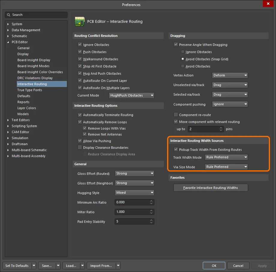
Параметры Interactive Routing Width Sources определяют, какой размер используется при начале маршрута.
Обратите внимание, что Track Width Mode установлен в Rule Preferred на изображении. Это означает, что когда трассировка начинается на существующем объекте цепи, например на площадке, будет использоваться именно эта ширина. Однако если трассировка начинается на существующей дорожке, то параметр Pickup Track Width From Existing Routes переопределит Track Width Mode и установит новую ширину так, чтобы она соответствовала существующей ширине.
Как разработчик, вы также можете нажать сочетание Shift+W во время трассировки, чтобы открыть диалог, где можно выбрать другую ширину, либо нажать Tab, чтобы открыть Properties panel и ввести новое значение Width . Выбранное или введенное значение должно находиться между настройками Min и Max, определенными в применимом правиле. Если нет, оно автоматически будет ограничено до ближайшего из этих значений.
Горячие клавиши интерактивной трассировки
Во время трассировки доступен ряд горячих клавиш. Например, можно нажать Shift+R, чтобы циклически переключаться между доступными режимами разрешения конфликтов, или нажать Backspace, чтобы удалить последнюю размещенную вершину (угол). Чтобы отобразить список горячих клавиш во время трассировки, нажмите Shift+F1. Отобразится меню доступных интерактивных горячих клавиш; выберите нужную команду или нажмите Esc, чтобы закрыть меню и использовать последовательность горячих клавиш.

Во время интерактивной трассировки нажмите Shift+F1, чтобы отобразить меню доступных интерактивных горячих клавиш
Перемещение дорожки
Подменю Edit » Move и меню команд перемещения в Active Bar содержат ряд команд, которые можно использовать для изменения положения или формы дорожки.

Re-Route
Эта команда позволяет вручную переложить (reroute) уже существующую дорожку на плате. После запуска команды курсор изменится на перекрестие, и вам будет предложено выбрать дорожку. Наведите курсор на нужную дорожку, затем щелкните или нажмите Enter. Работа этой функции зависит от того, включена ли опция Preserve Angle When Dragging на странице PCB Editor - Interactive Routing page диалогового окна Preferences:
-
Preserve Angle Dragging enabled - дорожка будет разорвана с добавлением нового сегмента для сохранения ортогональных/диагональных соединений. Перемещайте курсор, чтобы сдвинуть этот сегмент как требуется, затем щелкните для размещения. На этом этапе щелкните правой кнопкой или нажмите Esc , иначе новый сегмент будет разорван с добавлением следующего сегмента. Используйте сочетание клавиш Shift+R, чтобы циклически переключать варианты, определяющие, как следует обрабатывать препятствия при перетаскивании (Ignore Obstacles, Avoid Obstacles или Avoid Obstacles (Snap Grid)). Если включен один из режимов Avoid Obstacles, при перетаскивании будут соблюдаться правила, не позволяя перетащить сегмент так, чтобы возникло нарушение.
-
Preserve Angle Dragging disabled - оба конца сегмента дорожки будут зафиксированы, и вы сможете прокладывать новые сегменты дорожки между ними. Щелкните или нажмите Enter для размещения нового сегмента дорожки. Продолжайте размещать новые сегменты для переложения или щелкните правой кнопкой или нажмите Esc для остановки.
Продолжайте переложение других дорожек или щелкните правой кнопкой или нажмите Esc для выхода.
-
Если включен Preserve Angle Dragging, вы можете временно отключить его, удерживая клавишу Alt перед щелчком по целевому сегменту дорожки. Продолжайте удерживать клавишу Alt , последовательно щелкая для переложения.
-
При переложении дорожки этой командой и при отключенном Preserve Angle Dragging рекомендуется начинать переложение с левого конца выбранного сегмента дорожки и двигаться к правому.
-
Похожую функциональность переложения можно получить, выбрав сегмент дорожки, затем щелкнув и перетащив его центральную вершину. Далее выполняйте щелчок-и-перетаскивание центральных вершин получающихся сегментов вдоль исходной дорожки от одного конца к другому.
Break Track
Эта команда позволяет создать вершину (или разрыв) в сегменте дорожки. После запуска команды курсор изменится на перекрестие, и вам будет предложено выбрать дорожку. Наведите курсор на нужный сегмент дорожки в той точке сегмента, где вы хотите вставить разрыв, затем щелкните или нажмите Enter. Вставляется вершина, фактически разделяя исходный сегмент на два.
Переместите вершину в требуемое положение, затем щелкните или нажмите Enter для размещения. Присоединенные сегменты дорожки ведут себя в соответствии с настройкой опции Preserve Angle When Dragging на странице PCB Editor - Interactive Routing page диалогового окна Preferences:
-
Preserve Angle When Dragging enabled — углы к соседним сегментам дорожки сохраняются, поддерживая стиль трассировки.
-
Preserve Angle When Dragging disabled — два отдельных сегмента дорожки будут «на резинке» (rubber band), чтобы компенсировать перемещение, не сохраняя существующий стиль трассировки.
Продолжайте разрывать другие сегменты дорожек или щелкните правой кнопкой или нажмите Esc для выхода.
Также можно разорвать сегмент дорожки в текущей позиции курсора, используя сочетание клавиш Shift+Ctrl+Click&Hold.
Drag Track End
Эта команда позволяет вручную перепозиционировать или перетаскивать конец проложенного сегмента дорожки. После запуска команды курсор изменится на перекрестие, и вам будет предложено выбрать объект. Наведите курсор на дорожку, затем щелкните или нажмите Enter. Курсор «прыгнет» к ближайшему концу сегмента дорожки, и конец дорожки будет привязан к курсору. Переместите конец дорожки в нужное положение, затем щелкните или нажмите Enter для размещения.
-
Если конец выбранного сегмента дорожки — это вершина, к которой не подключены другие сегменты дорожек, переместите вершину в требуемое положение.
-
Если конец выбранного сегмента дорожки — это вершина, к которой подключены два сегмента дорожек, присоединенные сегменты будут «на резинке» по мере перемещения вершины.
-
Если конец сегмента дорожки подключен к площадке компонента, перемещение конца отсоединит его от площадки. После перепозиционирования конца будет показана логическая линия соединения от конца дорожки к площадке, при условии что опция Smart Track Ends включена на странице PCB Editor – General page диалогового окна Preferences.
-
Если конец сегмента дорожки подключен к свободной площадке, площадка будет привязана к курсору для перепозиционирования. Все дорожки, подключенные к площадке, будут соответствующим образом «на резинке».
-
Если конец сегмента дорожки подключен к переходному отверстию (via), via будет привязано к курсору для перепозиционирования. Все дорожки, подключенные к via, будут соответствующим образом «на резинке».
Продолжайте перетаскивать другие концы дорожек или щелкните правой кнопкой или нажмите Esc для выхода.
-
Эта команда переопределяется, если опция Preserve Angle When Dragging включена на странице PCB Editor - Interactive Routing page диалогового окна Preferences.
-
Эту функцию также можно вызвать, сначала выбрав нужную дорожку, а затем щелкнув и перетащив требуемую конечную вершину.
Move / Resize Tracks
Эта команда используется для перемещения конечных точек нескольких выбранных сегментов дорожек, фактически изменяя размер сегментов. После запуска команды курсор изменится на перекрестие, и вам будет предложено выбрать конечную точку дорожки. Чтобы переместить/изменить размер дорожек:
-
Наведите курсор на конечную точку одного из сегментов в выделении, затем щелкните или нажмите Enter.
-
Перемещайте курсор; все сегменты дорожек в выделении будут динамически изменять размер, сохраняя исходные расстояния и углы между собой. Другой конец каждого сегмента будет «на резинке», чтобы сохранить существующее соединение/расположение.
-
Когда сегменты окажутся в нужном месте, щелкните или нажмите Enter , чтобы выполнить размещение и выйти из режима перемещения.
-
Чтобы отменить операцию, щелкните правой кнопкой или нажмите Esc.
Во время перемещения сегментов доступны следующие дополнительные элементы управления:
-
Нажмите клавишу Tab , чтобы циклически переключать курсор между конечными точками каждого сегмента дорожки в выделении.
-
Удерживайте клавишу Alt при перемещении, чтобы ограничить движение в определенном направлении в зависимости от первоначального направления перемещения. Возможны направления по горизонтали, по вертикали и под углом 45 градусов.
-
Нажмите Spacebar дважды, чтобы быстро выровнять все конечные точки сегментов дорожек по одной линии либо по горизонтали, либо по вертикали. Нажмите Spacebar еще раз дважды быстро, чтобы вернуться к предыдущему размеру.
Эту команду также можно использовать для перемещения конечной точки одного, невыделенного сегмента дорожки. Обратите внимание: в этом случае можно использовать только дополнительное управление клавишей Alt .
Slicing Tracks
Инструмент Track Slicer предоставляет простой механизм для разрезания одного или нескольких сегментов дорожек на две части и может разрезать дорожки на текущем сигнальном слое или на всех видимых сигнальных слоях. Чтобы открыть инструмент, выберите команду Edit » Slice Tracks в главном меню.
После запуска команды курсор изменится на перекрестие, и вам будет предложено выбрать начальную точку разреза. Кроме того, применяется фильтрация, чтобы в рабочей области отображались только объекты дорожек. Это будут либо все дорожки на всех видимых сигнальных слоях, либо только дорожки на текущем сигнальном слое — в зависимости от активной настройки Track Slicer. Чтобы разрезать одну или несколько дорожек:
-
Расположите курсор и щелкните или нажмите Enter, чтобы зафиксировать начальную точку разреза.
-
Переместите курсор через точку дорожки или дорожек, где нужно выполнить разрез, — траектория резака отображается линией, а предполагаемые разрезы визуально показываются.
-
Щелкните или нажмите Enter, чтобы зафиксировать конечную точку линии резака.
-
Продолжайте разрезать другие сегменты дорожек или щелкните правой кнопкой или нажмите Esc для выхода из режима разрезания.
Дополнительные действия, которые можно выполнять после выбора начальной точки разреза и во время перемещения «линии разреза», следующие:
-
Сегмент дорожки разрезается так, что границы лезвия проходят через точки, которые станут центрами «горячих точек» (hotspots) двух получившихся концов сегментов.
-
Ширину режущего лезвия можно свободно задать в диалоге Slicer Properties. Либо можно ограничить ширину лезвия, привязав её к текущей сетке Snap. Если значение Blade Width не кратно сетке Snap, оно будет обрезано так, чтобы попасть в сетку. Получившаяся ширина называется Gridded Width. Если этот параметр отключён AND и Blade Width не кратен текущей сетке Snap, один или оба получившихся конца сегментов дорожки могут оказаться вне сетки. Если Blade Side установлено в Left или Right, конец дорожки на границе лезвия будет расположен вне сетки (конец дорожки вдоль оси начальной точки останется в сетке). Если Blade Side установлено в Both, тогда оба конца дорожки окажутся вне сетки.
-
Параметр Blade Side управляет тем, как выполняется разрез относительно оси, определяемой выбранной начальной точкой разреза. В рабочем поле ось, определяемая выбранной начальной точкой, отображается сплошной линией, а границы лезвия — пунктирной линией. Доступны следующие варианты:
-
Left — разрез будет выполнен слева от оси начальной точки. Расстояние разреза будет равно полной Blade Width или Gridded Width (в зависимости от применимого).
-
Right — разрез будет выполнен справа от оси начальной точки. Расстояние разреза будет равно полной Blade Width или Gridded Width (в зависимости от применимого).
-
Both — разрез будет выполнен поровну слева и справа от оси начальной точки. Расстояние разреза с каждой стороны будет равно половине полной Blade Width или половине Gridded Width (в зависимости от применимого).
-
Включите параметр Cut Current Layer Only , чтобы разрезать только сегменты дорожек на текущем слое. Отключите этот параметр, чтобы разрезать сегменты дорожек на всех видимых слоях, если эти сегменты попадают в «траекторию» Track Slicer.
-
Степень маскирования при применённой фильтрации в рабочей области можно вручную настроить с помощью ползунка Dimmed Objects, расположенного в разделе Mask and Dim Settings на вкладке View Options панели View Configuration. Сбросьте фильтрацию с помощью сочетания клавиш Shift+C .
Преобразование дорожек в фасонный (chamfered) путь
Снятие фаски на 90‑градусных углах трассировки — это приём, используемый для уменьшения отражений, вызванных углом на СВЧ‑трассе. Можно использовать дуги — но их радиус должен быть как минимум в 3 раза больше ширины трассы. Снятие фаски (также называемое mitering) — альтернативный подход, при котором срезается внешняя вершина угла. Поскольку объекты дорожек в Altium Designer имеют скруглённые окончания, их нельзя использовать для создания угла со снятой фаской. Чтобы создать такой угол, выбранные сегменты дорожек заменяются объектами region.
Выберите все сегменты дорожек, для которых нужно снять фаску, затем выполните команду Tools » Convert » Convert Selected Tracks to Chamfered Path в главном меню. Откроется диалог Convert Tracks to Chamfered Path. Используйте этот диалог для настройки фаски, затем нажмите OK. Каждая выбранная пара сегментов дорожек (с проблемными 90‑градусными углами) будет заменена на угол со снятой фаской, а исходные сегменты дорожек в каждой паре будут преобразованы в один сплошной (медный) объект region.
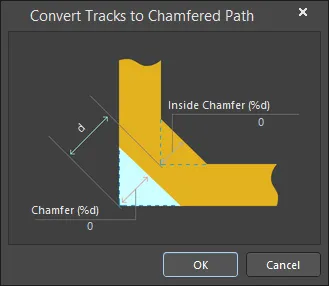
Выбранные дорожки будут обработаны фаской на заданную величину в каждом прямом угле.
Используйте следующие параметры диалога для настройки фаски:
-
Chamfer — величина внешнего угла, который нужно срезать (снять фаску), в процентах от существующей диагональной дистанции угла.
-
Inside Chamfer — количество материала, добавляемого во внутренний угол в процентах от существующей диагональной дистанции угла.
How big should the Chamfer be?
Процент митра (percentage mitre) — это доля среза диагонали между внутренним и внешним углами изгиба без митра.

Оптимальный митр для широкого диапазона геометрий микрополосковых линий был экспериментально определён Douville и James. Они установили, что хорошее приближение для оптимального percentage mitre задаётся выражением

При условии  и при диэлектрической проницаемости подложки
  .
.
Эта формула полностью не зависит от  . Фактический диапазон параметров, для которого Douville и James приводят подтверждения, составляет
  и
и  . Они сообщают о VSWR лучше 1.1 (т.е. обратные потери лучше −26 dB) для любого percentage mitre в пределах 4% (от исходного
  ) от значения, полученного по формуле. При минимальном
  0.25 percentage mitre составляет 98.4%, то есть полоса практически полностью прорезается.
Процесс снятия фаски преобразует несколько сегментов дорожек в один объект region. Это необратимый процесс: после преобразования дорожек в region их нельзя преобразовать обратно. Поэтому снятие фаски следует выполнять только после завершения всей трассировки. Если вы не уверены, сохраните копию платы перед снятием фаски.
Track Properties

Режим Track панели Properties.
Информация о цепи (Net Information)
Этот раздел содержит сведения о цепи, к которой относится дорожка, а также о дифференциальной паре и/или xSignal, если эта цепь является участником. При необходимости отображается информация о классе. Также приводятся значения Delay, Length, Max Current и Resistance.
См. страницу PCB Placement & Editing Techniques, чтобы узнать больше об информации о цепях.
Расположение (Location)
Значок

справа от этого раздела должен отображаться как

(разблокировано) , чтобы получить доступ к полям ниже. Нажмите значок блокировки/разблокировки, чтобы изменить его состояние.
-
(X/Y)
-
X
(первое поле) — текущая координата X (горизонтальная) опорной точки дорожки относительно текущего начала координат рабочего пространства. Отредактируйте, чтобы изменить положение дорожки по X. Значение можно вводить как в метрических, так и в дюймовых единицах; указывайте единицы при вводе значения, если они отличаются от текущих единиц по умолчанию.
-
Y
(второе поле) — текущая координата Y (вертикальная) опорной точки дорожки относительно текущего начала координат. Отредактируйте, чтобы изменить положение дорожки по Y. Значение можно вводить как в метрических, так и в дюймовых единицах; указывайте единицы при вводе значения, если они отличаются от текущих единиц по умолчанию.
Свойства (Properties)
-
Component
— это поле отображается в PCB editor только когда выбранная дорожка (Track) является составной частью PCB Component, и показывает позиционное обозначение родительского PCB‑компонента. Выберите кликабельную ссылку Component, чтобы открыть режим Component панели Properties для родительского компонента.
-
Net
— используется для выбора цепи (net) для дорожки. Все цепи активного проекта платы будут перечислены в выпадающем списке. Обратите внимание: если размещение объекта начинается в той же точке, что и существующий объект, уже подключённый к цепи, то свойство Net нового объекта автоматически назначается этой цепи. Выберите No Net , чтобы указать, что дорожка не подключена ни к одной цепи. Свойство Net примитива используется Design Rule Checker для определения, корректно ли размещён объект PCB. Также можно нажать значок Assign Net (
 ), чтобы выбрать объект в рабочем поле — цепь этого объекта будет назначена выбранной дорожке(ам).
-
Layer
— используйте выпадающий список, чтобы выбрать слой, на котором расположена дорожка.
-
Width
— отображает текущую ширину дорожки. Отредактируйте это поле, чтобы изменить ширину дорожки в диапазоне от 0.001mil до 10000mil.
-
Start (X/Y)
— отображает текущую координату X/Y начальной точки дорожки относительно текущего начала координат.
-
End (X/Y)
— отображает текущую координату X/Y конечной точки дорожки относительно текущего начала координат.
-
Length
— отображает текущую длину дорожки. Отредактируйте это поле, чтобы изменить длину дорожки в диапазоне от 0.001mil до 10000mil.
Значения можно задавать в мм или mil. При вводе значения в единицах, отличных от текущих, добавьте к значению суффикс mm или mil.
Расширение паяльной пасты (Paste Mask Expansion)
-
Rule/Manual
— выберите нужную конфигурацию расширения маски пасты. Выберите Rule, чтобы расширение маски пасты для дорожки следовало значению, заданному в соответствующем правиле проектирования Paste Mask Expansion. Выберите Manual, чтобы переопределить соответствующее правило проектирования и задать значение расширения маски пасты для дорожки. После этого можно включить параметр и ввести нужное значение.
Расширение паяльной маски (Solder Mask Expansion)
-
Rule/Manual– выберите требуемую конфигурацию расширения паяльной маски. Выберите Rule, чтобы расширение паяльной маски для дорожки соответствовало заданному значению в применимом правиле проектирования Solder Mask Expansion . Выберите Manual, чтобы переопределить применимое правило проектирования и указать значение расширения паяльной маски для дорожки. После этого можно включить параметр и ввести нужное значение.
Работа с дугами
Дуга — это примитивный объект проектирования. По сути, это круговой сегмент дорожки, который можно размещать на любом слое. Дуги могут использоваться в разводке печатной платы по-разному. Например, их можно применять при определении контуров компонентов на слоях оверлея или на механическом слое для обозначения контура платы, границ вырезов и т. п. Также их можно использовать для создания криволинейных трасс при интерактивной трассировке. Дуги могут быть открытыми или замкнутыми, образуя окружность (часто это называют дугой полного круга).

Две размещённые дуги; слева — дуга полного круга, справа — дуга, выбранная для редактирования.
Дуги доступны для размещения как в редакторе PCB, так и в редакторе библиотек PCB. Доступны четыре режима размещения дуг (Center, Edge, Any Angle и Full Circle). Способ размещения дуги зависит от выбранного метода:
-
Place arc by center – этот метод позволяет разместить дугу, используя центр дуги в качестве начальной точки.
После запуска команды курсор изменится на перекрестие, и вы перейдёте в режим размещения дуги. Размещение выполняется следующей последовательностью действий:
-
Щёлкните или нажмите Enter, чтобы зафиксировать центральную точку дуги.
-
Переместите курсор, чтобы настроить радиус дуги, затем щёлкните или нажмите Enter, чтобы задать его.
-
Переместите курсор, чтобы настроить начальную точку дуги, затем щёлкните или нажмите Enter, чтобы зафиксировать её.
-
Переместите курсор, чтобы изменить положение конечной точки дуги, затем щёлкните или нажмите Enter, чтобы зафиксировать её и завершить размещение дуги.
-
Продолжайте размещать следующие дуги или щёлкните правой кнопкой мыши либо нажмите Esc, чтобы выйти из режима размещения.
-
Place arc by edge – этот метод позволяет разместить дугу, используя край дуги в качестве начальной точки. Угол дуги фиксирован и равен 90°.
После запуска команды курсор изменится на перекрестие, и вы перейдёте в режим размещения дуги. Размещение выполняется следующей последовательностью действий:
-
Щёлкните или нажмите Enter, чтобы зафиксировать начальную точку дуги.
-
Переместите курсор, чтобы изменить положение конечной точки дуги, затем щёлкните или нажмите Enter, чтобы зафиксировать её и завершить размещение дуги.
-
Продолжайте размещать следующие дуги или щёлкните правой кнопкой мыши либо нажмите Esc, чтобы выйти из режима размещения.
-
Place arc by edge (any angle) – этот метод позволяет разместить дугу, используя край дуги в качестве начальной точки. Угол дуги может быть любым.
После запуска команды курсор изменится на перекрестие, и вы перейдёте в режим размещения дуги. Размещение выполняется следующей последовательностью действий:
-
Щёлкните или нажмите Enter, чтобы зафиксировать начальную точку дуги.
-
Переместите курсор, чтобы настроить радиус дуги, затем щёлкните или нажмите Enter, чтобы зафиксировать центральную точку.
-
Переместите курсор, чтобы изменить положение конечной точки дуги, затем щёлкните или нажмите Enter, чтобы зафиксировать её и завершить размещение дуги.
-
Продолжайте размещать следующие дуги или щёлкните правой кнопкой мыши либо нажмите Esc, чтобы выйти из режима размещения.
-
Place full circle arc – этот метод позволяет разместить дугу 360° (полный круг).
После запуска команды курсор изменится на перекрестие, и вы перейдёте в режим размещения дуги. Размещение выполняется следующей последовательностью действий:
-
Щёлкните или нажмите Enter, чтобы зафиксировать центральную точку дуги.
-
Переместите курсор, чтобы настроить радиус дуги, затем щёлкните или нажмите Enter, чтобы задать его и завершить размещение дуги.
-
Продолжайте размещать следующие дуги или щёлкните правой кнопкой мыши либо нажмите Esc, чтобы выйти из режима размещения.
Дополнительные действия, которые можно выполнять во время размещения:
-
Для всех методов (кроме дуг полного круга) нажмите Spacebar перед заданием конечной точки дуги, чтобы построить дугу в противоположном направлении.
-
Нажмите клавишу L, чтобы перенести дугу на другую сторону платы — обратите внимание, что это возможно только до фиксации начальной/центральной точки дуги.
-
Нажмите клавиши + и - (на цифровой клавиатуре) или используйте сочетания Shift+Ctrl+Wheelroll, чтобы циклически переходить вперёд и назад по всем видимым слоям в проекте и быстро менять слой размещения.
Графический метод редактирования позволяет выбрать размещённую дугу непосредственно в рабочей области и графически изменить её размер, форму или положение.
Когда объект дуги выбран, доступны следующие маркеры редактирования:

Выбранная дуга
-
Щёлкните и перетащите A, чтобы изменить радиус.
-
Щёлкните и перетащите B, чтобы изменить конечные точки (начальный и конечный углы).
-
Щёлкните в любом месте дуги вдали от маркеров редактирования, затем перетащите, чтобы переместить её. Либо щёлкните и перетащите центральную точку дуги. Во время перетаскивания дугу можно поворачивать или зеркалировать:
-
Нажмите Spacebar, чтобы повернуть дугу против часовой стрелки, или Shift+Spacebar — по часовой стрелке. Поворот выполняется в соответствии со значением Rotation Step, заданным на странице PCB Editor – General диалога Preferences.
-
Нажмите клавиши X или Y, чтобы отзеркалить дугу относительно оси X или оси Y.
Arc Properties

Режим Arc панели Properties.
Информация о цепи
Этот раздел предоставляет информацию о цепи, к которой относится дуга, а также о дифференциальной паре и/или xSignal, если эта цепь является участником. При необходимости отображается информация о классе. Также приводятся значения Delay, Length, Max Current и Resistance.
Чтобы узнать больше об информации о цепях, см. страницу PCB Placement & Editing Techniques.
Расположение
Значок

справа от этого раздела должен отображаться как

(разблокировано), чтобы получить доступ к полям ниже. Нажмите значок блокировки/разблокировки, чтобы изменить его состояние.
-
(X/Y)
-
X (первое поле) — это поле показывает текущее положение X центра дуги относительно текущего начала координат. Измените значение в поле, чтобы изменить положение дуги относительно текущего начала координат. Значение можно вводить как в метрических, так и в дюймовых единицах; указывайте единицы измерения при вводе значения, если они отличаются от текущих единиц по умолчанию. Единицы по умолчанию (метрические или дюймовые) определяются параметром Units в области Other панели Properties в режиме Board (доступен, когда в рабочей области не выбраны объекты) и используются, если единицы не указаны.
-
Y (второе поле) — это поле показывает текущее положение Y центра дуги относительно текущего начала координат. Измените значение в поле, чтобы изменить положение дуги относительно текущего начала координат. Значение можно вводить как в метрических, так и в дюймовых единицах; указывайте единицы измерения при вводе значения, если они отличаются от текущих единиц по умолчанию. Единицы по умолчанию (метрические или дюймовые) определяются параметром Units в области Other панели Properties в режиме Board (доступен, когда в рабочей области не выбраны объекты) и используются, если единицы не указаны.
Свойства
-
Component – это поле отображается в редакторе PCB только когда выбранная дуга является составной частью PCB-компонента и показывает обозначение родительского PCB-компонента. Выберите кликабельную ссылку Component, чтобы открыть режим Component панели Properties для родительского компонента.
-
Net– используется для выбора цепи (net) для дуги. Все цепи активного проекта платы будут перечислены в раскрывающемся списке. Обратите внимание: если размещение объекта начинается в той же точке, что и существующий объект, уже подключенный к цепи, то свойство Net нового объекта автоматически назначается этой цепи. Выберите No Net, чтобы указать, что дуга не подключена ни к одной цепи. Свойство Net примитива используется средством Design Rule Checker для определения, корректно ли размещён объект PCB. Либо можно щёлкнуть по значку Assign Net (), чтобы выбрать объект в рабочей области — цепь этого объекта будет назначена выбранной дуге (дугам).
-
Layer - это поле отображает слой, к которому в данный момент назначена дуга. Дуги можно назначать на любой доступный слой. Чтобы изменить назначенный слой, щёлкните поле и выберите слой из раскрывающегося списка.
-
Width - это поле отображает ширину линии дуги. При необходимости введите другое значение ширины.
-
Radius - это поле отображает радиус дуги, измеренный от центральной точки до центра линии дуги. При необходимости введите другое значение радиуса.
-
Start Angle - это поле отображает начальный угол дуги, измеренный от оси X в первом квадранте (плоская геометрия). При необходимости введите другое значение начального угла.
-
End Angle - это поле отображает конечный угол дуги. При необходимости введите другое значение конечного угла.
-
Propagation Delay - это поле отображает время, за которое сигнал распространяется вдоль данного маршрута.
Paste Mask Expansion
-
Rule - выберите, чтобы расширение паяльной пасты (paste mask) для дуги следовало значению, заданному в соответствующем правиле проектирования Paste Mask Expansion. Связанное значение расширения будет отключено, если выбран этот параметр.
-
Manual - выберите, чтобы переопределить соответствующее правило проектирования и задать значение расширения paste mask для дуги в поле ниже.
Solder Mask Expansion
-
Rule - установите флажок, чтобы расширение паяльной маски (solder mask) для дуги следовало значению, заданному в соответствующем правиле проектирования Solder Mask Expansion. Связанное значение расширения будет отключено, если выбран этот параметр.
-
Manual - установите флажок, чтобы переопределить соответствующее правило проектирования и задать значение расширения solder mask для дуги в поле ниже.
Обводка выбранных объектов дорожками и дугами
Команда Tools » Outline Selected Objects из главного меню может использоваться для размещения контура из дорожек и дуг вокруг выбранных свободных примитивов в проекте. Эта функция может быть особенно полезна, если нужно электрически изолировать критические цепи, привязав контур к источнику земли. После запуска команды объекты будут обведены дорожками и/или дугами. Контурные дорожки/дуги размещаются с шириной 8 mil, а свойство Net устанавливается в No Net.
Соблюдаются правила проектирования Clearance, Width и Short-Circuit для данного проекта, поэтому нарушения зазоров будут отмечены средством Design Rule Checker.
Работа с прямоугольниками
Прямоугольник можно разместить на любом слое. Прямоугольники разных размеров можно комбинировать, чтобы покрывать области неправильной формы, а также сочетать с сегментами дорожек или дуг.
Прямоугольники также можно размещать на неэлектрических слоях. Например, разместите прямоугольник на слое Keep-Out, чтобы обозначить «запретную» область для автотрассировки. Разместите прямоугольник на слое Power Plane, Solder Mask или Paste Mask, чтобы создать вырез (void) на этом слое.

Размещённый прямоугольник
Прямоугольники доступны для размещения как в редакторе PCB, так и в редакторе библиотек PCB следующими способами:
-
PCB Editor — доступны следующие способы:
-
Выберите Place » Rectangle в главном меню.
-
Нажмите кнопку Rectangle (
 ) в раскрывающемся списке на Active Bar, расположенной в верхней части рабочей области. (Нажмите и удерживайте кнопку Active Bar, чтобы получить доступ к другим связанным командам. После использования команды она станет верхним пунктом в этом разделе Active Bar.)
-
Щёлкните правой кнопкой мыши в рабочей области, затем выберите Place » Rectangle в контекстном меню.
-
PCB Library Editor — доступны следующие способы:
-
Выберите Place » Rectangle в главном меню.
-
Нажмите кнопку Rectangle () в раскрывающемся списке на Active Bar, расположенной в верхней части рабочей области. (Нажмите и удерживайте кнопку Active Bar, чтобы получить доступ к другим связанным командам. После использования команды она станет верхним пунктом в этом разделе Active Bar.)
-
Щёлкните правой кнопкой мыши в рабочей области, затем выберите Place » Rectangle в контекстном меню.
После запуска команды курсор изменится на перекрестие, и вы перейдёте в режим размещения прямоугольника. Размещение выполняется следующей последовательностью действий:
-
Щёлкните или нажмите Enter, чтобы зафиксировать первый угол прямоугольника.
-
Переместите курсор, чтобы настроить размер прямоугольника, затем щёлкните или нажмите Enter, чтобы зафиксировать диагонально противоположный угол и завершить размещение прямоугольника.
-
Продолжайте размещать следующие прямоугольники либо щёлкните правой кнопкой мыши или нажмите Esc, чтобы выйти из режима размещения.
Дополнительные действия, доступные во время размещения:
-
Нажмите клавишу Tab, чтобы приостановить размещение и получить доступ к режиму Rectangle mode панели Properties , где можно на лету изменять свойства. Нажмите наложенную кнопку паузы в рабочей области (
 ), чтобы продолжить размещение.
-
Нажмите Spacebar , чтобы циклически переключать различные режимы углов. Выберите Rectangle для прямых углов, Fillet для скруглённых углов или Chamfer для скошенных/наклонных углов.
-
Нажимайте клавиши + и - (на цифровой клавиатуре), чтобы циклически переходить вперёд и назад по всем видимым слоям проекта и быстро менять слой размещения.
-
Нажмите и удерживайте клавишу Alt, чтобы ограничить направление перемещения по горизонтальной или вертикальной оси в зависимости от первоначального направления движения.
Хотя атрибуты можно изменять во время размещения (
Tab — чтобы открыть панель
Properties ), имейте в виду, что они станут настройками по умолчанию для дальнейшего размещения, если не включена опция
Permanent на странице
PCB Editor – Defaults диалога
Preferences. Когда эта опция включена, внесённые изменения будут влиять только на размещаемый объект и последующие объекты, размещаемые в рамках той же сессии размещения.
Графический способ редактирования позволяет выбрать размещённый прямоугольник непосредственно в рабочей области и графически изменить его размер, форму или положение.
Когда объект-прямоугольник выбран, доступны следующие маркеры редактирования.
 Выбранный прямоугольник
-
Щёлкните и перетащите углы (A), чтобы изменять размер прямоугольника одновременно по вертикали и горизонтали.
-
Щёлкните и перетащите центры сторон (B), чтобы изменять размер прямоугольника по вертикали и горизонтали отдельно.
-
Щёлкните в любом месте прямоугольника вдали от маркеров редактирования и перетащите, чтобы переместить его. Во время перетаскивания прямоугольник можно поворачивать или зеркалировать:
-
Нажмите Spacebar, чтобы повернуть прямоугольник против часовой стрелки, или Shift+Spacebar — по часовой стрелке. Поворот выполняется в соответствии со значением Rotation Step, заданным на странице PCB Editor – General диалога Preferences.
-
Нажмите клавиши X или Y, чтобы отзеркалить прямоугольник относительно оси X или оси Y.
Чтобы преобразовать объект Rectangle в исходный набор примитивов, выберите команду
Tools » Convert » Explode Rectangle to Free Primitives в главном меню. Хотя отдельной команды для повторной группировки «взорванного» прямоугольника нет, для этого можно использовать команду
Undo.
Rectangle Properties

Режим Rectangle панели Properties.
Расположение
Значок замка справа от этой области должен отображаться как разблокированный для доступа к полям ниже. Переключайте значок блокировки/разблокировки, чтобы изменить его состояние.
-
(X/Y)
-
X (первое поле) — текущая координата X (по горизонтали) опорной точки прямоугольника относительно текущего начала координат рабочего пространства. Отредактируйте, чтобы изменить положение прямоугольника по X. Значение можно вводить как в метрических, так и в дюймовых единицах; указывайте единицы при вводе значения, если они отличаются от текущих единиц по умолчанию.
-
Y (второе поле) — текущая координата Y (по вертикали) опорной точки прямоугольника относительно текущего начала координат. Отредактируйте, чтобы изменить положение заливки по Y. Значение можно вводить как в метрических, так и в дюймовых единицах; указывайте единицы при вводе значения, если они отличаются от текущих единиц по умолчанию.
-
Rotation — угол поворота прямоугольника (в градусах), измеряемый против часовой стрелки от нуля (по 3 o'clock горизонтали). Отредактируйте, чтобы изменить поворот прямоугольника. Минимальное угловое разрешение — 0,001°.
Свойства
-
Corner Mode — используйте выпадающий список, чтобы выбрать нужный режим углов прямоугольника из следующих вариантов:
-
Rectangle — задаёт, что размещаемый прямоугольник будет с прямыми (квадратными) углами.
-
Fillet — задаёт, что размещаемый прямоугольник будет со скруглёнными углами.
-
Chamfer — задаёт, что размещаемый прямоугольник будет со скошенными или наклонными углами.
Режим углов также можно выбрать во время размещения, нажав Spacebar.

 Локализовано с помощью ИИ