在进行 PCB 设计时,可使用多种对象。放置在 PCB 文档中的大多数对象都会定义铜区域或挖空区域。这既适用于走线、焊盘等电气对象,也适用于文本、标注等非电气对象。因此,务必注意用于定义每个对象的线宽,以及对象所放置的层。
PCB 编辑器中的对象分为两类——基本对象(Primitive objects)和组对象(Group objects):
对象放置与编辑的共性
在 Altium Designer 中,无论放置哪种对象,放置流程大体相同。最简单的流程如下:
-
从某个工具栏或 Place 菜单中选择要放置的对象。
-
使用鼠标在 PCB 编辑器设计空间中定义对象的放置位置及其尺寸(如适用)。
-
右键单击(或按 Esc)以终止命令并退出放置模式。
对象会放置在当前层上。放置前请确保已将正确的层设为当前层。对象放置后也可以更改其所在层。
放置前编辑
可随时在 PCB Editor – Defaults 页面的 Preferences 对话框中更改对象的默认属性。这些属性会在后续放置对象时应用。

使用 Primitives 列访问各对象的属性,并按需编辑默认值。
默认情况下,对象的默认值保存在文件 ADVPCB.dft 中。也可以选择将值保存到名称不同的 .dft 文件中。提供了保存和加载 .dft 文件的控件,使你能够创建常用的默认对象值“集合”。所有保存在 .dft 文件中并从中加载的设置均为用户自定义默认值。如有需要,可随时使用 Set To Defaults 或 Reset All 选项恢复原始默认值。原始默认值为硬编码。
放置过程中编辑
对象首次放置时可编辑多项属性。要访问这些属性,请在放置模式下按 Tab 键打开关联的 Properties面板。按下 Tab 键会暂停放置,以便你对对象进行所需编辑。

Pad 对象的属性对话框示例。
完成编辑后,单击设计空间中的暂停按钮叠加层(  )以继续放置。
以这种方式设置的属性将成为后续对象放置的默认设置,除非在
Preferences 对话框的
PCB Editor – Defaults 页面启用了
Permanent 选项。启用该选项后,所做更改仅影响正在放置的对象以及同一次放置会话中后续放置的对象。
放置后编辑
对象放置完成后,可通过多种方式进行编辑。如下所述。
关联的属性面板或对话框
此编辑方法使用关联的 Properties面板模式和对话框来修改已放置对象的属性。
放置后,可通过以下方式打开关联对话框:
放置后,可通过以下方式之一访问 Properties面板的关联模式:
-
如果 Properties面板已处于活动状态,选择该对象即可。
-
选择对象后,通过设计空间右下角的 Panels按钮选择 Properties面板,或从主菜单中选择 View » Panels » Properties。
如果在
Preferences对话框的
PCB Editor – General page 中禁用了
Double Click Runs Interactive Properties选项(默认),当双击基本对象,或在选中基本对象后右键并选择
Properties 时,将打开对话框。启用
Double Click Runs Interactive Properties选项后,将打开
Properties面板。
尽管对话框与面板中的选项相同,但选项的顺序与布局可能略有差异。
按 Ctrl+Q 可在面板/对话框中切换当前使用的度量单位:公制(mm)与英制(mil)。这只影响面板/对话框中的测量显示,不会更改板子的测量单位;板子的单位在设计空间未选中任何对象时,通过 Properties面板中的 Units设置进行配置。
PCB 对象选择命令
除 标准对象选择/取消选择命令 外,PCB 编辑器还提供了多种特殊命令,以便进行对象选择/取消选择操作。这些命令可从主菜单的 Edit » Select 和 Edit » DeSelect 子菜单中访问。也可从 Active Bar 中的  按钮菜单访问这些选择命令。
-
Select overlapped - 用于在一组同位置(重叠)的对象中,单步选择下一个设计对象,而无需使用选择弹出窗口。选择遵循以下固定优先级顺序,并在连续使用该命令时循环切换:
-
焊盘
-
过孔
-
走线/圆弧
-
元件
-
多边形
-
区域/填充
-
文本
此外,在使用 Shift 键将更多对象加入当前选择时,你可以使用 Shift+Tab 在重叠对象之间循环选择,而不会丢失原有选择。
-
要使用此命令,请确保在 Preferences对话框的 PCB Editor - General page 中禁用 Display popup selection dialog 选项。
-
选择顺序还会优先考虑当前层,然后才会切换到其他层上的对象。
-
在重叠对象区域双击始终会打开弹出式选择窗口。
-
Select next (快捷键:Tab)- 在设计中已选中一个初始对象的情况下,此命令用于按逻辑层级将选择扩展到下一个更高层级的对象(或对象组)。支持以下循环的逻辑选择“流”:
-
走线段 ---> 同层所有相连(连续)走线 ---> 所有相连铜 ---> 关联网络中的所有电气对象
-
相连焊盘 ---> 同层所有相连(连续)走线 ---> 所有相连铜 ---> 关联网络中的所有电气对象
-
未连接焊盘 ---> 关联网络中的所有电气对象
-
过孔 ---> 与过孔关联层上的所有相连(连续)走线 ---> 所有相连铜 ---> 关联网络中的所有电气对象
-
铜(区域/多边形覆铜/填充) ---> 所有相连铜 ---> 关联网络中的所有电气对象
-
自由焊盘/过孔 ---> 与焊盘同层、或与过孔关联层上的所有相连(连续)走线 ---> 所有相连铜 ---> 关联网络中的所有电气对象。
-
元件 ---> 过孔扇出、逃逸、互连
Via Fanouts - 如果一条足够短的走线将焊盘连接到过孔,并且没有其他焊盘通过更短的走线连接到该过孔,则该走线与过孔被视为该焊盘的 Fanout。
Escapes - 连接到焊盘的、足够短的天线(antenna)被视为该焊盘的 Escape。
Interconnect - 连接两个已被拾取对象(例如焊盘或扇出过孔)的走线被视为 Interconnect。
此外,该功能还支持跨多个对象扩展选择,这些对象可分布在设计中的不同网络上。

跨多个网络的选择示例:从最初选中的走线段开始,沿更高阶的逻辑层级向上扩展。
该命令在选择已布线网络时尤其有用。了解更多:Strategies for Selecting the Routing。
-
Board - 用于选择位于已定义板框边界内的所有对象。
-
Net - 用于选择与特定网络关联的所有电气对象。
启动该命令后,你可以单击某个电气对象或连接,以选择其所属网络(net)中的所有电气对象;或者,如果你知道要选择的网络名称,可在设计中远离任何对象的区域单击,Net Name 对话框将打开。在该对话框中输入所需的网络名称;关闭对话框后,该网络将被选中。如果你不确定网络名称,请输入 ?,然后单击 OK 以打开 Nets Loaded 对话框,该对话框会列出此设计当前已加载的所有网络。

-
Connected Copper - 用于选择连接到同一段铜皮的所有电气对象。
-
Physical Connection - 用于选择焊盘对象之间所有已实际布线的走线。单击一段走线、焊盘或过孔;直到遇到另一个焊盘为止的所有连续走线都会被选中,包括其中的任何过孔(焊盘本身不会包含在选择中)。
-
Physical Connection Single Layer - 用于在单一层上选择焊盘对象之间所有已实际布线的走线。单击一段走线或过孔;同一层上直到遇到另一个焊盘为止的所有连续走线都会被选中(焊盘和过孔本身不会包含在选择中)。
-
Component Connections - 用于选择从所选元件的焊盘引出的所有已布线连接(包括走线和过孔),并在每条连接上一直选到下一个遇到的焊盘为止。焊盘本身不会包含在选择中。
也可以通过在已放置的元件上右键单击,然后从上下文菜单中选择 Component Actions » Select Component Connections 命令来访问该命令。
-
Component Nets - 用于选择当前文档中连接到所选元件的所有网络(以及其中的网络成员对象)。
也可以通过在已放置的元件上右键单击,然后从上下文菜单中选择 Component Actions » Select Component Nets 命令来访问该命令。
-
Room Connections - 用于选择当前文档中完全位于所选 Room 边界内的所有焊盘到焊盘的已布线连接。
也可以通过在已放置的 Room 上右键单击,然后从上下文菜单中选择 Room Actions » Select Room Connections 命令来访问该命令。
-
All on Layer - 用于选择/取消选择当前层上的所有对象。
元件可能放置在某一层上,但可能无法使用 DeSelect » All on Layer 命令将其取消选择。这是因为构成元件的并非所有图元都放置在同一层上。例如,位号和注释文本可能放在 Top Overlay 层,而组成焊盘则是 Multi-Layer。
-
Free Objects - 用于选择设计中的所有自由图元对象。元件对象、坐标对象、尺寸标注对象、长度调谐对象、OLE 对象以及多边形覆铜对象都属于组对象,因此不会受此命令影响。
-
All Locked - 用于选择所有启用了 Locked 属性的设计对象。
-
Off Grid Pads - 用于选择所有未放置在当前捕捉栅格上的焊盘。
请注意,在 PCB 编辑器中,Lasso Select / Lasso Deselect 命令提供两种操作模式:
-
Free-form - 类似真正的套索,你可以手绘自由形状的选择区域,以包含所需的设计对象。
-
Polyline - 提供多边形“套索”,当需要更精确地取消选择对象时,该模式可能比自由形状模式更合适。该模式在元件以 45 度旋转的设计中,或在处理柔性板(flex)且设计并非总是正交时非常有用。
你甚至可以组合使用两种模式,使取消选择区域完全符合你的需求。当前模式会显示在 Status Bar 中。按 Spacebar 可在 Free-form 与 Polyline 模式之间切换。
在使用 Lasso Select、Inside Area、Outside Area、Touching Line 或 Touching Rectangle 命令时按住 Ctrl 键,可将目标定位到元件对象的图元。
图形化编辑
这种编辑方法允许你在设计空间中直接选择已放置的对象,并以图形方式更改其大小、形状或位置。形状和/或尺寸(如适用)的修改通过对象被选中后出现的编辑“句柄”来完成。
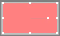
选中的 Fill 对象的编辑句柄示例。
在对象上任意位置单击(避开编辑句柄,如存在)即可拖动对象以重新定位。根据对象类型,在拖动时还可以旋转和/或翻转。
-
按 Spacebar 可逆时针旋转对象,或按 Shift+Spacebar 顺时针旋转。旋转角度遵循 Preferences 对话框中 PCB Editor – General 页面 里定义的 Rotation Step 值。
-
按 L 键可将对象翻转到电路板的另一面(如适用)。
-
按 X 或 Y 键可使对象沿 X 轴或 Y 轴翻转(如适用)。
-
按 Alt 键可根据初始移动方向,将移动方向约束为水平或垂直轴。
-
按住 Ctrl 键并按方向键,可按小步长(依据当前捕捉栅格值)微移对象。按住 Ctrl+Shift 键并按方向键,可按更大步长(10 倍捕捉栅格值)微移。
移动命令
对象位置可通过主菜单中的 Edit » Move 子菜单或 Active Bar 中的移动子菜单命令来更改。

-
Move - 该命令用于移动当前文档中的任意对象。与对象相关联的任何网络将保持连接,连接线会在对象移动时跟随(是否显示取决于当前生效的连接模式)。与对象相连的任何已布线走线不会被移动。
-
Drag - 该命令用于移动当前文档中的任意对象。如果对象连接了走线和/或圆弧(例如元件、焊盘或过孔),在移动对象时这些连接将保持相连。
-
要让与元件相连的走线随元件一起移动,必须在 Preferences 对话框的 PCB Editor - General page 中将 Comp Drag 模式设置为 Connected Tracks。如果该模式设置为 None,该命令的行为将与基本移动命令相同。
-
当使用此命令拖动元件且 Comp Drag 模式设置为 Connected Tracks 时,旋转与翻转的快捷键命令将不可用。另请注意,智能移动操作(动态对齐与推挤)也不可用。
-
Component - 该命令使你能够移动当前文档中的元件。启动命令后,在设计中单击要移动的元件,将其移动到所需位置后再单击确认。或者,在设计空间中远离任何对象的位置单击以打开 Choose Component dialog。使用该对话框定位要移动的元件(可跳转到该元件,或将元件带到光标处),然后按上述方式重新定位。注意:仅当目标元件处于 not locked 状态时,此功能才会工作。
也可以通过在设计空间中的元件上右键单击,然后从上下文菜单中选择 Component Actions » Move Component 命令来访问该命令。
-
Move Selection - 该命令使你能够在当前文档中手动重新定位所选对象。选择中与对象相关联的任何网络将保持连接,连接线会在对象移动时跟随(是否显示取决于当前生效的连接模式)。与对象相连的任何已布线走线不会被移动。
-
Move Selection by X, Y - 该命令用于将当前所选对象按 X 和/或 Y 方向精确偏移一定量。启动命令后将打开 Get X/Y Offsets 对话框。使用该对话框指定用于移动选择对象的 delta X 和/或 delta Y 增量值。
仅当设计空间中至少选中了一个对象时,该命令才可用。

Get X/Y Offsets 对话框
获取 X/Y 偏移对话框的选项与控件
-
X Offset - 使用此字段指定所选对象沿水平轴移动的距离。可根据所需移动方向指定正值或负值。使用该字段右侧的按钮可快速在正/负值之间切换已输入的数值。
-
Y Offset - 使用此字段指定所选对象沿垂直轴移动的距离。可根据所需移动方向指定正值或负值。使用该字段右侧的按钮可快速在正/负值之间切换已输入的数值。
-
Toggle X/Y Offsets - 单击此按钮可快速交换偏移值。X Offset 值将用作 Y Offset 值,反之亦然。
-
Reset X/Y Offsets - 单击此按钮可快速将两个偏移值重置为零。
-
Define X/Y Offsets Interactively - 单击此按钮可交互式计算偏移量。系统将带你返回工作区,并依次提示选择起点和终点。在所需位置单击;dX 和 dY 值将分别填入 X Offset 和 Y Offset 字段。
要在英制与公制之间切换对话框单位,请按 Ctrl+Q 快捷键。
-
Rotate Selection - 此命令用于在设计空间中将所选对象按指定旋转角度逆时针或顺时针旋转。启动命令后,将打开 Rotation Angle (Degrees) 对话框。输入所需旋转角度(0.001° 到 360.00°,分辨率 0.001°)。输入正值表示逆时针旋转,输入负值表示顺时针旋转。单击 OK 关闭对话框,然后定位光标并单击以定义旋转参考点。所选对象将围绕该参考点按输入角度旋转。

Rotation Angle 对话框
-
Flip Selection - 将所选对象水平翻转(绕 Y 轴)到电路板另一侧的对应层。例如,位于 Top Layer 上的对象将翻转到 Bottom Layer,位于 Top Overlay 上的对象将翻转到 Bottom Overlay,等等。
-
翻转后,Designator 和 Comment 文本会变为镜像。
-
对于存在于 Multi-Layer 上的焊盘,翻转本质上会反转其 XY 尺寸配对与形状的顺序。因此,如果使用了 Top-Middle-Bottom 的样式且形状最初为 Round-Rectangle-Octagonal,翻转将反转堆叠顺序,从而使自顶层起的形状变为 Octagonal-Rectangle-Round。
-
如果选择了多个对象,则该对象集合将围绕选择集的几何中心进行翻转。
请注意,除非一个或多个对象的位置被锁定,否则所有选定对象都会在无警告的情况下被翻转。在这种情况下,将出现 Confirm 对话框,需要确认后才会翻转对象。
对齐命令
也可以通过更改对齐方式来移动对象。要将对象与其他对象对齐,请在选定对象上单击右键,然后选择 Align。或者,使用主菜单中的 Edit » Align 子菜单,或 Active Bar 中的对齐子菜单。对齐子菜单包含多种用于分布所选对象的选项。
对齐命令只会移动可自由移动的已选对象——被锁定的对象不会移动。

Align 命令用于访问 Align Objects 对话框,该对话框提供控件,可按需快速对齐当前选定的一组设计对象。使用该对话框根据需要为所选对象设置 Vertical 和/或 Horizontal 对齐选项,然后单击 OK 执行对齐。

Align Objects 对话框
-
同时启用 Horizontal 和 Vertical 选项可能会产生冲突,导致所选对象彼此堆叠在一起。
-
使用 Space equally 选项可能会导致被移动的对象偏离网格。
对齐对象对话框的选项与控件
-
Horizontal - 从以下选项中选择一个,以确定所选对象的水平对齐方式:
-
No Change - 保持对象的水平对齐不变。
-
Left - 对齐对象,使其最左侧图元的外边缘具有相同的 X 位置。以最左侧图元所在的对象作为参考。
-
Center - 水平移动对象,使其中心对齐。单击 OK 后, 系统会提示你单击选择参考对象。
-
Right - 对齐对象,使其最右侧图元的外边缘具有相同的 X 位置。以最右侧图元所在的对象作为参考。
-
Space equally - 对象在水平方向上等间距分布,位于最左与最右对象之间(这两个对象不移动)。
-
Vertical - 从以下选项中选择一个,以确定所选对象的垂直对齐方式:
-
No Change - 保持所选对象的垂直对齐不变。
-
Top - 对齐对象,使其最上侧图元的外边缘具有相同的 Y 位置。以最上侧图元所在的对象作为参考。
-
Center - 垂直移动对象,使其中心对齐。单击 OK 后,系统会提示你单击选择参考对象。
-
Bottom - 对齐对象,使其最下侧图元的外边缘具有相同的 Y 位置。以最下侧图元所在的对象作为参考。
-
Space equally - 对象在垂直方向上等间距分布,位于最上与最下对象之间(这两个对象不移动)。
Position Component Text 命令用于运行 Component Text Position 对话框,你可以在其中更改当前文档中一个或多个所选元件的 Designator 和/或 Comment 文本位置。

Component Text Position 对话框
该对话框基本分为两个区域——Designator 与 Comment 文本。对于 Designator 和 Comment,都会使用元件的图形表示作为辅助,以显示在所选位置下文本将出现的位置。文本提供以下九种位置样式,均归类为“自动位置”,这意味着当元件移动和旋转时,文本会保持在所选位置:
-
Left-Above
-
Left-Center
-
Left-Below
-
Center-Above
-
Center
-
Center-Below
-
Right-Above
-
Right-Center
-
Right-Below
若要保持文本在当前位置且不做修改,请保持 No Change 选项启用。
-
Designator 和 Comment 文本位置也可通过 Properties 面板中的 Properties 区域进行更改。选择 Designator/Comment 或其父元件即可显示这些属性。单击相应控件(以文字汇总当前 Designator/Comment 的层、位置与旋转),然后在弹出窗口中按需使用 Autoposition 属性。
-
若要自由定位 Designator/Comment 文本并使其跟随父元件的移动/方向,请在 Properties 面板中配置属性时,为 Autoposition 属性选择 Manual 样式。你也可以在工作区中直接单击、按住并拖动文本到所需位置;这将自动把 Autoposition 属性切换为 Manual。
Align Left / Align Right / Align Top / Align Bottom 命令使你能够分别按左/右/上/下边缘对齐所选设计对象。 启动命令后,将以最左/最右/最上/最下对象的左/右/上/下边缘作为参考,并将选择中的所有其他对象向左/右/上/下移动,使其左边缘与该参考对齐。
Align Left (maintain spacing) / Align Right (maintain spacing) / Align Top (maintain spacing) / Align Bottom (maintain spacing) 命令使你能够在遵守适用设计规则并保持足够间距的情况下,按左/右/上/下边缘对齐所选设计对象。启动命令后,将以最左/最右/最上/最下对象的左/右/上/下边缘作为参考,并将选择中的所有其他对象向左/右/上/下移动,使其左边缘与该参考对齐。 对象将尽可能靠近参考对象地向左/右/上/下移动,移动距离以适用的间隙规则允许为限:
Align Horizontal Centers / Align Vertical Centers 命令可将所选对象排列到同一列/行中,并按其水平/垂直中心对齐。启动该命令后,光标将变为十字准星,并提示你在所选对象中选择其中一个对象;单击该对象。它将成为参考对象。所选中的其他所有对象都会相对于该参考对象移动,并按其水平/垂直中心对齐。
Distribute Horizontally / Distribute Vertically 命令用于使一组选定对象的水平/垂直间距相等。启动该命令后,所选对象中最左与最右 / 最上与最下的对象将保持位置不变,其余对象将在它们之间等距分布。对象的垂直/水平位置不会改变。
Increase Horizontal Spacing / Increase Vertical Spacing 命令用于增大一组选定对象的水平/垂直间距。启动该命令后,最左/最下的对象将保持固定,而所选中的其他对象将向右/向上移动。移动方式为:相邻对象参考点之间的水平/垂直距离将按 Step X / Step Y 字段中为默认 Global Board Snap Grid 指定的数值增加。
Decrease Horizontal Spacing / Decrease Vertical Spacing 命令用于减小一组选定对象的水平/垂直间距。启动该命令后,最左/最下的对象将保持固定,而所选中的其他对象将向左/向下移动。移动方式为:相邻对象参考点之间的水平/垂直距离将按 Step X / Step Y 字段中为默认 Global Board Snap Grid 指定的数值减少。
Align To Grid 命令用于将所选元件移动到适用且已修改的捕捉网格(snap grid)上的最近点。启动该命令后,每个所选元件的参考点将移动到适用捕捉网格上的最近点。
Move All Components Origin To Grid 命令用于将所有元件的参考点移动到当前 Snap Grid 上。启动该命令后,设计空间中所有焊盘在网格上的元件都会被移动,使其参考点与当前捕捉网格对齐。默认情况下,会自动生成并打开一份报告(Move Component(s) Origin To Grid - <PCBDocumentName>.html)作为活动文档,详细说明哪些元件已移动、哪些未移动。
注意:焊盘当前不在网格上的元件不会被移动。
通过 PCB List Panel
PCB List panel 允许你以表格形式显示设计对象,从而快速检查并修改对象属性。与 PCB Filter 面板配合使用时,它可仅显示处于活动过滤器范围内的对象——从而更准确、更高效地定位并编辑多个设计对象。
选择活动层
活动层是你将要放置对象的层。可通过单击设计空间底部该层的标签,从当前可见层中选择活动层;也可使用 View Configuration 面板的 Layers & Colors 选项卡中 Layers 区域的 Active Layer 下拉列表进行选择。
你也可以使用以下快捷键快速选择活动层:
放置在多层(multi-layer)上的对象会自动出现在所有信号层上。
使用剪切/复制与粘贴
在 PCB 编辑器中,你可以在同一 PCB 文档内或不同 PCB 文档之间剪切/复制并粘贴对象,例如可将某个 PCB 中的元件复制到另一个 PCB 文档中。你可以将对象剪切/复制到 Windows 剪贴板,并将其粘贴到其他文档中。
使用 2D Layout Mode 时,选择要剪切/复制的对象,然后从主菜单单击 Edit » Cut(Ctrl+X)/ Edit » Copy(Ctrl+C),或从右键菜单选择 Cut/Copy 命令。光标将变为十字准星,并提示你选择一个参考点。该参考点是相对于所选对象的坐标,用于在执行粘贴命令时精确定位所选内容。
在 3D Layout Mode 中使用 Copy 命令时,设计空间中的当前视图将以位图格式复制到剪贴板。你可以通过随后打开的 3D Snapshot Resolution 对话框控制复制图像的分辨率。
要将当前选中的设计对象以文本格式复制到剪贴板,可使用主菜单中的 Edit » Copy As Text 命令。随后可将这些信息粘贴到任意文本字段或外部文本文档中。复制到剪贴板的细节包括:
-
对象类型。
-
位号与注释(针对元件对象)。
-
对象在设计空间中的位置。
-
对象所在层(或过孔的起始层与终止层)。
将元件以文本形式复制到剪贴板的示例如下:
Component Y1-25MHz (100.6mm,1.5mm) on Top Layer
将走线与过孔以文本形式复制到剪贴板的示例如下:
Track (20mm,6mm)(80mm,6mm) Top Layer
Via (45mm,6mm) Top Layer to Bottom Layer
要将最后一次剪切/复制到剪贴板的内容放置到活动文档中,请从主菜单或在设计空间内右键并从上下文菜单选择 Edit » Paste 命令,或选择 Paste 命令(快捷键:Ctrl+V)。最新的剪贴板内容将以悬浮方式跟随光标显示。光标相对于该内容的位置由使用 Cut 或 Copy 将所选内容添加到剪贴板时指定的参考点决定。
使用 Paste 命令时,对象会被粘贴到源对象被复制时所在的同一层上,而不受编辑器当前设置为活动层的影响。
要将从受支持的 OLE 应用程序复制的文本放置到任意打开的 PCB 文档中,可使用主菜单中的 Edit » Paste Text 命令。该文本会被转换为 PCB 字符串对象并粘贴,而不是作为单个 OLE 对象粘贴。支持的文件类型包括通用格式,例如 CSV 与 XLS 格式的电子表格,以及 DOC 与 RTF 的文字文档。
要控制某些对象属性在粘贴回设计空间时的处理方式,可使用主菜单中的 Edit » Paste Special 命令。启动该命令后,将打开 Paste Special 对话框。

Paste Special 对话框
Options and Controls of the Paste Special Dialog
Paste Attributes
-
Paste on current layer - 启用此选项可将对象粘贴到当前层。
-
Keep net name - 启用此选项可保留对象的原始网络名称。
-
Duplicate designator - 启用此选项可在不自动递增的情况下,粘贴具有相同位号的元件。
-
Add to component class - 启用此选项可将粘贴的元件加入与源元件相同的元件类(component class)。
当剪贴板中包含已复制的源元件时,Duplicate designator 与 Add to component class 选项将可用。
Buttons
根据所粘贴内容的具体类型,可控制以下属性:
按需设置选项,然后单击 Paste 按钮以开始粘贴操作。
在 Paste Special 对话框中单击 Paste Array 按钮将打开 Setup Paste Array 对话框,该对话框允许你将剪贴板对象的多个副本粘贴到当前文档中。

Setup Paste Array 对话框
Options and Controls of the Setup Paste Array Dialog
放置变量
-
Item Count - 要执行的重复放置次数。例如,输入 4 将放置当前剪贴板内容的 4 个副本。
-
Text Increment - 输入显示文本(例如元件或焊盘标号)的自动递增量。支持字母与数字递增,且递增步长不必为 1。例如,在将焊盘复制到剪贴板之前先设置其标号,并设置 Text Increment 字段后,可放置如下类型的焊盘标号序列:
-
数字(1、3、5)
-
字母(A、B、C)
-
字母与数字组合(A1、A2,或 1A、1B,或 A1、B1,或 1A、2A 等)
-
若要按数字递增,将 Text Increment 字段设置为你希望每次递增的数值。
-
若要按字母递增,将 Text Increment 字段设置为字母表中代表你希望跳过字母数量的字母。例如,若初始焊盘标号为 1A,且 Text Increment 字段设置为 C(字母表第 3 个字母),则焊盘标号将为 1A、1D(A 之后第 3 个字母)、1G(D 之后第 3 个字母),依此类推。
-
注意:在粘贴阵列后,会记住上次使用的递增值;除非你执行新的 Copy 操作,否则下一次粘贴阵列时,将使用该序列中的下一个值作为新阵列的基值。
阵列类型
-
Circular- 启用此选项可使用当前 Circular Array 设置粘贴圆形阵列。
-
Linear - 启用此选项可使用当前 Linear Array 设置以直线方式粘贴阵列。
圆形阵列
-
Rotate Item to Match - 若启用,阵列项将按与其间距相同的角度增量进行旋转。
-
Spacing (degrees) - 两个相邻粘贴项之间的角度间隔。
线性阵列
-
X-Spacing - 输入两个相邻项目之间所需的 X 方向间距。
-
Y- Spacing - 输入两个相邻项目之间所需的 Y 方向间距。
粘贴阵列时,将使用执行 Copy 操作时所用的同一参考位置来“抓取”阵列。
在此对话框中输入适当的数值,然后单击 OK 以放置阵列。
-
如果放置线性阵列,系统会提示你选择阵列的起始点。定位光标后单击 或按 Enter 以放置阵列。
-
如果放置圆形阵列,系统会提示你先选择阵列的中心点,然后选择阵列的起始点。每一步都将光标定位后单击 或按 Enter 以放置阵列。对象将围绕指定中心点按逆时针方向放置。
阵列的起始点将是参考点所在的位置——该参考点是在使用 Cut 或 Copy 将所选内容添加到剪贴板时指定的。因此,建议在剪切/复制时正确指定参考点,否则在粘贴阵列时可能出现意外结果。
要在当前文档中复制一个或多个已选对象,并在需要的位置粘贴该选择的多个实例,也可以使用主菜单中的 Edit » Duplicate 命令(快捷键:Ctrl+R)。启动该命令后,光标将变为十字准星,并进入重复模式。流程包含以下步骤:
-
首先会提示你选择一个参考点。该点将作为粘贴选择内容时的基准点。将光标移动到选择内容附近的所需位置,然后单击 或按 Enter。选择内容的一个副本将跟随光标悬浮显示。
-
将光标移动到设计空间中的目标位置,然后单击 或按 Enter 放置该副本。
-
另一个副本将再次跟随光标悬浮显示,准备放置。
-
继续放置更多已复制选择的实例(有点像使用橡皮图章) 或右键单击 或按 Esc 退出。
注意:该命令用于复制并粘贴对象。因此,你不能用该命令来复制组对象的子对象。
Priorities When Pasting Objects
当在铜层上粘贴对象时,如果粘贴后与一组不同类型的对象发生重叠,则会将优先级最高对象的网络分配给被粘贴对象。优先级如下(1 为最高优先级):
-
焊盘
-
填充
-
区域
-
走线
-
圆弧
-
过孔
-
多边形覆铜
粘贴到一组不同类型、且分配了不同网络的对象之上。由于焊盘是该组中优先级最高的对象,因此其网络(Pad_Net)将分配给被粘贴对象。将光标悬停在图像上可查看结果。")
优先级最高对象的网络会分配给被粘贴对象。此处展示了一个对象(走线)粘贴到一组不同类型、且分配了不同网络的对象之上。由于焊盘是该组中优先级最高的对象,因此其网络(Pad_Net)将分配给被粘贴对象。将光标悬停在图像上可查看结果。
当在铜层上粘贴对象时,如果粘贴后与一组相同类型的对象发生重叠,则会将你单击以粘贴对象时光标下方对象的网络分配给被粘贴对象。
粘贴到一组相同类型的对象(焊盘)之上。由于在单击粘贴时光标下方的是焊盘 2,因此该焊盘的网络(Pad2_Net)将分配给被粘贴对象。将光标悬停在图像上可查看结果。")
光标下方对象的网络会分配给被粘贴对象。此处展示了一个对象(走线)粘贴到一组相同类型的对象(焊盘)之上。由于在单击粘贴时光标下方的是焊盘 2,因此该焊盘的网络(Pad2_Net)将分配给被粘贴对象。将光标悬停在图像上可查看结果。
当在铜层上粘贴一组物理连接的对象时,如果该组中不同类型的对象与具有不同网络的现有对象发生重叠,则该组中优先级最高对象的网络将分配给所有被粘贴对象。此情况下同样适用上述优先级规则。
粘贴到分配了不同网络的对象(过孔)之上。由于填充是该粘贴组中优先级最高的对象,因此分配给它的网络(Via1_Net)将分配给该组中的每个对象。将光标悬停在图像上可查看结果。")
分配给优先级最高对象的网络会分配给这组物理连接的对象。此处展示了一组连接对象(从左到右:填充、区域、走线、圆弧、过孔、多边形覆铜)粘贴到分配了不同网络的对象(过孔)之上。由于填充是该粘贴组中优先级最高的对象,因此分配给它的网络(Via1_Net)将分配给该组中的每个对象。将光标悬停在图像上可查看结果。
锁定设计对象
通过启用其 Locked 属性,可以防止 PCB 文档中的设计对象被移动或编辑。例如,如果某些对象的位置或尺寸至关重要,就应将其锁定。可在 Properties 面板中,通过单击目标对象旁的挂锁图标( )来完成锁定,如下例所示。

Lock 图标在 Properties 面板中针对已选元件与焊盘的示例。
要切换已放置对象的 Locked 属性状态(该对象具有 Locked 属性),也可以在设计空间中右键单击该对象,并从上下文菜单中选择 <ObjectType> Locked 命令。 当对象已被锁定时,菜单中的该命令条目左侧会显示一个勾选图标。
如果你尝试移动或旋转已启用 Locked 属性的设计对象,将弹出对话框要求确认是否继续编辑。
如果在 Preferences 对话框的 PCB Editor – General 页面中启用了 Protect Locked Objects 选项,且设计对象已锁定,则该对象无法被选择或进行图形化编辑。请使用 Properties 面板上的 Lock 图标解锁对象,或禁用 Protect Locked Objects 选项以对该对象进行图形化编辑。
如果你尝试将锁定对象与其他对象一起选择,则在启用 Protect Locked Objects 选项时,只有未锁定的对象可以被选中并作为一组移动。
元件图元锁定
如果 PCB 元件的图元被锁定(Properties 面板的 Component 模式中的 Primitives 选项处于  状态),则这些图元的全部或大多数属性无法通过图形化(例如拖放)和非图形化(例如使用 Properties 或 List 面板)编辑方式进行修改。这有助于防止对元件图元的偶发更改,从而避免导致装配与制造输出不正确。
举例来说,下图显示了一个焊盘的 Properties 面板的 Pad 模式;该焊盘是某个 PCB 元件的组成部分,并且该元件的 primitives 已被锁定。请注意,焊盘的所有属性(除 Net 和 Testpoint 属性外)都会变灰,且无法编辑。还要注意,在焊盘的 Component 字段最右侧会显示  图标,这表示其父元件的 primitives 已锁定,因此无法修改焊盘属性。
显示效果(右侧)。")
对于 primitives 已锁定的 PCB 元件,其焊盘在 Properties 面板的 Pad 模式(左侧)显示效果(右侧)。
重入式编辑
PCB Editor 包含一项强大的功能,称为 re-entrant editing。它允许在不终止当前操作的情况下,通过键盘快捷键执行第二个操作。重入式编辑让你的工作方式更灵活、更直观。例如,假设你开始放置一段走线,随后意识到必须删除另一段走线段。此时无需退出 Interactive Routing 模式。按下 E、D 快捷键,删除所需的走线段,然后按 Esc 键即可返回交互式布线状态,继续对设计进行交互式布线。
设置 PCB 光标外观
默认情况下,PCB 光标为一个小的绿色 90 度十字。你可以在 Preferences dialog 的 PCB Editor – General 页面中,通过 Cursor Type 和 Cursor Color 设置进行配置。例如,延伸到设计窗口边缘的大型 90 度十字(Large 90 选项)在放置与对齐设计对象时会很有用。或者,如果 90 度选项在网格线背景下不易看清,45 度十字(Small 45 选项)可能更适合。
True Type 字体支持
PCB Editor 支持在设计中的文本相关对象(文本字符串/边框、尺寸标注、钻孔表和/或层叠表)使用基于笔画(Stroke-based)或 TrueType 字体。字体的选择在相应的 Properties panel 中完成。提供三种基于笔画的字体选项:Default、Sans Serif 和 Serif。Default 样式是一种简单的矢量字体,支持笔式绘图(pen plotting)和矢量光绘(vector photoplotting)。Sans Serif 和 Serif 字体更复杂,会降低矢量输出(例如 Gerber)的生成速度。基于笔画的字体内置于软件中,无法更改。这三种字体都包含完整的 IBM 扩展 ASCII 字符集,支持英语及其他欧洲语言。使用 TrueType 字体时,可使用 \Windows\Fonts 文件夹中找到的 TrueType 与 OpenType(TrueType 的超集)字体。该功能还提供完整的 Unicode 支持。
请注意,只有被检测到(且名称唯一)的根字体才可用。例如,Arial 和 Arial Black 可用,但 Arial Bold 和 Arial Bold Italic 不可用。
使用 TrueType 字体的文本对象几何形状会自动存储在 PCB 文档中。当 PCB 文档中的对象使用 TrueType 字体时,即使在另一台电脑上打开该 PCB 文档且未安装该 TrueType 字体,这些对象仍会以相同的字体几何形状显示。
当选择了使用缺失字体的对象时,Properties panel 顶部会出现警告信息。当更改会影响其文本的对象属性(例如文本高度或文本内容本身)时,会打开 Missing fonts dialog,你可以在其中选择替代字体(Replacement)。启用 Apply to all text elements 选项可将替代字体应用到 PCB 文档中所有使用该缺失字体的对象。

当从 PCB List panel 更改文本相关属性时,也会出现该对话框。
当尝试编辑多个使用不同缺失字体的对象时,该对话框允许你为每一种缺失字体分别选择替代字体。

在 Advanced Settings dialog 中启用 PCB.Text.TTFontSaving 选项后,即可使用“将使用 TrueType 字体的文本对象几何形状自动存储到 PCB 文档中”的功能。当该选项被禁用时,你可以配置 Altium Designer 以嵌入 TrueType 字体。Preferences dialog 的 PCB Editor – TrueType Fonts 页面(当 Advanced Settings dialog 中的 PCB.Text.TTFontSetting.Hide 选项被禁用时可用)提供了 Embed TrueType fonts inside PCB documents 选项,用于在保存设计时嵌入 TrueType 字体;并提供 Substitution font 选项,用于在加载设计时应用所选的字体替换。
当需要以某种字体显示文本,而目标电脑在加载设计时可能安装也可能未安装该字体时,嵌入字体会很有用。字体替换则允许在加载设计时指定一个 TrueType 字体作为替代字体,适用于未嵌入字体且当前加载设计的电脑上可能缺少相关字体的情况。
网络信息
对于 PCB 上的铜对象(走线、过孔、多边形等),当选中对象时,Properties panel 的 Net Information 区域会显示以下信息:
-
其父级 Net、Diff Pair 和/或 xSignal,以及各自关联的类(class)。注意,只有当对象分别属于差分对或 xSignal 时,才会显示 Diff Pair 和 xSignal 条目。
-
Delay – 所选对象的延迟,以及整个网络已布线段的延迟。若已为焊盘和过孔定义了 Propagation Delay 值,则也会包含焊盘与过孔的 Propagation Delay 值。
对于过孔,传播延迟会按所用过孔长度成比例计算。该功能在 Advanced Settings dialog 中启用 PCB.Delay.Via 选项时可用。当 PCB.Delay.Via 选项被禁用时,将使用在过孔属性中定义的 Propagation Delay 值。
-
Length – 所选对象的总长度之和,以及总 Signal Length。Signal Length 是对总节点到节点距离的精确计算。系统会分析已放置对象,以:解析堆叠或重叠对象以及焊盘内的游走路径;并将过孔长度计入其中。若已为焊盘定义 Pin Package Length,也会将其包含在内。如果该网络未完全布线,还会包含连接线的曼哈顿(X + Y)长度。有关信号长度及其应用的更多信息,请参阅关于 PCB - Nets panel 的说明。
-
总长度包含对网络未布线部分的估算(连接线的曼哈顿(X + Y)长度),但总延迟不包含该估算部分。
-
对于属于已定义 Supply Nets design rule(或属于与该规则一起使用的网络类)的网络,不计算其 Delay 和 Length。
-
Max Current - 所选 Track、Arc 或 Via 对象可承载的最大电流,根据 IPC-2221A 公式(第 6.2 节)确定:
I = k * ΔT0.44 * A0.725
其中:
I = 电流 [A]
A = 横截面积 [平方 mil](走线宽度 * 层叠铜厚,或如下所示的 Abarrel)
ΔT = 允许的环境温升 [°C]
k = 常数,其中:
k = 0.048(外层)
k = 0.024(内层)
当选择多个对象(例如整个网络)时,该网络的最大电流取所选对象中各自最大电流值的最小值。
-
Resistance - 所选 Track、Arc 和 Via 对象的电阻之和,根据推导公式确定:
R = (ρ * L / A)
其中:
R = 电阻 [Ω]
ρ = 铜的电阻率 [Ω*mm2/m]
L = 走线长度 [m] (或如下所述的 Via Length)
A = 横截面积 = T * W [mm2] (或如下所示的 Abarrel)
T = 走线厚度(来自层叠)[mm]
W = 走线宽度 [mm]
Assumptions:
-
环境温度 = 22 °C
-
允许温升 = 20 °C
-
通孔铜壁厚度 = 0.018mm
-
铜的电阻率 = 0.017 Ω*mm2/m
Via Barrel Cross-Sectional Area - 按如下方式确定:

Abarrel = AViaHoleSize - AFinishedHoleSize
Abarrel = [ π * (ViaHoleSize/2)2 ] - [ π * ((ViaHoleSize - 2 * ViaWallThickness)/2)2 ]
Abarrel = π (ViaHoleSize * ViaWallThickness - ViaWallThickness2)
Via Length = 从入口层中心到出口层中心的距离,如上所示
Notes - 这些计算中的过孔长度取决于该过孔是否属于某个网络,以及所连接走线所使用的层。未分配网络的所选过孔将显示“层边缘到层边缘”的长度,而不是“层中心到层中心”的长度。此外,已分配网络但没有连接走线的过孔将显示长度为零。

Properties面板的 Net Information 区域。此处显示的是所选走线的示例。
单击 Net Information 区域中的链接,可在 PCB 面板中打开关联的网络/差分对/xSignal。
为对象分配网络
PCB 编辑器提供了多种方式,可将网络分配给图元对象:
-
当选择了一个或多个对象时,使用 Properties 面板中 Nets 字段的下拉列表。活动板级设计中的所有网络都会列在下拉列表中。选择 No Net 以指定该走线不连接到任何网络。或者,你也可以单击 Assign Net 图标(
 )在设计空间中选择一个对象——该对象的网络将被分配给所选对象。
-
在一个或多个所选对象上右键单击,然后选择 Net Actions » Assign Net。启动命令后会出现十字光标。将十字光标悬停到你希望分配对象的网络上,然后单击以选择该网络。
-
要将布线图元的网络名称重新同步为其所连接焊盘上的网络名称,请从主菜单中选择 Design » Netlist » Update Free Primitives From Component Pads 命令。启动命令后,会打开确认对话框,询问是否要用元件焊盘网络更新自由图元网络。单击 Yes 后,并从每个焊盘开始,软件会选择相连的铜皮,并将每个图元的网络名称设置为与焊盘一致。此操作不会影响内部 PCB 网络表。
要检查并确认物理连接的对象是否被分配了正确的网络、从而属于该物理网络(此处 physical net 表示 connected copper),你可以使用 Configure Physical Nets 对话框:从主菜单中选择 Design » Netlist » Configure Physical Nets 命令即可访问。软件会分析设计,检查所有焊盘以及将它们物理连接在一起的对象(走线、圆弧、填充等)是否都分配了相同的网络名称。当某个网络中的所有对象都正确时,该网络会以绿色显示。如果检测到有对象相互接触但分配了不同的网络,则会以红色标记。一个常见情况是:元件封装内包含额外的铜对象。在同步加载该封装时,焊盘会应用分配的网络名称,但这些额外铜对象不会。该对话框是交互式的;单击某个网络或图元即可交叉定位到该对象。右键单击或单击 Menu 按钮可访问可用命令。对话框的 Action 区域提供控件,用于指定为解决相连铜皮问题需要采取的操作。默认情况下会自动设置操作,但也可按需调整。设置完成后,单击 Execute 按钮以更新网络分配。
请注意,此对话框的默认状态为 Only Show Errors,这意味着不会列出已正确分配的对象。要显示所有对象,请禁用 Only Show Errors 选项(使用 Menu 按钮),然后使用 Menu 按钮显示所有对象。
以及禁用 Only Show Errors 选项(前))。")
Configure Physical Nets 对话框(显示启用 Only Show Errors 选项(后)以及禁用 Only Show Errors 选项(前))。
Options and Controls of the Configure Physical Nets Dialog
-
Electrically Connected Copper - 此区域列出在设计布线中检测到的、彼此电气连接的铜图元的不同分组。对于每个分组,会显示以下信息:
-
Primitive - 在顶层,该条目反映相连铜皮中包含多少个图元。图元可以以扁平列表显示,或按图元类型分组显示。后者可通过启用 Menu 按钮选项中的 Show Primitive Groups 选项来配置。启用后,图元将被拆分为以下分组:
-
Connected Component Primitives - 将所有元件焊盘图元作为其子项列出。通过启用 Menu 按钮选项 Show Components,还可按父元件进一步分组。
-
Connected Free Primitives - 将所有非元件铜图元作为其子项列出,并按图元类型(填充、覆铜多边形、走线、过孔)进一步分组。
只有在“Menu”按钮选项中启用了 Show Component Pads 选项时,才会显示 Connected Component Primitives。同样,只有在启用了 Show Non Component Pads 选项时,才会显示 Connected Free Primitives。如果其中一个选项被禁用,顶层条目将反映当前隐藏了多少图元。如果这两个选项都被禁用,对话框将为空!对话框底部会出现 Show All Primitives 按钮,可快速显示所有图元(本质上是启用上述一个或两个被禁用的选项)。
单击某个图元条目会在设计空间中高亮该图元。选择多个图元条目将选中该选择中的所有图元。选择列表中的更高层级条目会使其所有后代子图元在工作区中被高亮。
-
Original Net Names - 此字段反映当前分配给该图元的网络名称,即该图元当前连接到的网络。该条目将是板上已定义网络之一。但是,如果某个图元未连接到网络,则该条目将为 <Unassigned>。
-
Status - 此字段为该分组提供一个顶层状态条目,可能处于以下四种状态之一:
-
Blank - 已连接铜皮分组的网络(net)分配完全正确,无需更新。该分组的顶层条目显示为绿色。
-
1. Update Required - Unassigned Nets - 在此状态下,分组中的所有图元(primitive)都尚未分配到任何网络。该分组的顶层条目显示为黄色。
-
2. Update Required - Some Unassigned Nets - 在此状态下,部分图元已分配到同一网络,但其他图元尚未分配。该分组的顶层条目显示为橙色。
-
3. Ambiguous - Multiple Net Names - 在此状态下,分组中存在被分配到不同网络的图元。也可能还有尚未分配的图元。该分组的顶层条目显示为红色。
-
Action - 此区域 提供用于指定解决已连接铜皮问题所需执行操作的控件,并显示执行所配置更改后的结果。对于每个分组,将显示以下内容:
-
Proposed Action - 此字段用于确定是否需要执行操作以及执行何种操作。在分组的最高层级,此条目可设置为 Update Net To 或 Don't Update Net To。更新时,请在 New Net Name 字段中选择新的目标网络。基于这两项设置,软件会计算在子图元层级需要执行的操作,并给出以下提议之一:
-
No Action Required - 该图元已分配/连接到目标网络。
-
Update - 将该图元纳入更新 使其分配/连接到新的目标网络。
-
Don't Update - 不将该图元纳入更新。它将保持连接到其当前网络。
-
New Net Name - 使用此字段设置图元应连接到的新目标网络。该字段的下拉列表会列出在该已连接铜皮分组的图元中检测到的所有网络。 如果需要使用不同的网络,请在该字段上右键并从上下文菜单中使用 Change Copper Net To Board Net 命令。这将打开 Choose Net 对话框,其中列出当前为电路板定义的所有网络。选择所需网络后点击 OK。该网络将被填入此字段。
-
Done - 当按下 Execute 按钮并应用更改后,此字段会反映更新操作的成功(
 )或失败(
)或失败( )。
)。
在父级层面切换提议的操作,会快速切换子级层面以及该父级下所有子项的提议操作。当各个子项的提议操作不一致——有的包含在更新中、有的被排除——则在分组图元层级结构中其上方的父级条目会以 Some Updates 来反映这种情况。
-
Execute - 当你对分配给网络表的操作满意后,点击 此按钮以更新网络分配。
-
Menu - 点击以访问以下命令菜单,这些命令与主列表整体或当前选中的图元相关。其命令与主列表区域右键菜单中提供的命令相同。
-
Show All Primitives - 点击此按钮可快速显示所有图元。如果菜单中的 Show Component Pads 和/或 Show Non Component Pads 选项被禁用,则此按钮可用。
你也可以 从当前设计文档中清除所有网络,本质上是清空内部 PCB 网络表。如果你已在源原理图文档中更改了网络信息,并希望让 PCB 与源原理图的网络表信息完全重新同步,这可能会很有用。要执行此操作, 请从主菜单选择 Design » Netlist » Clear All Nets 命令。 启动该命令后,会打开一个确认对话框,提醒你此操作将清除 PCB 中的所有网络信息。点击 Yes 后,所有网络信息将被移除。任何已布线的走线仍会保留布线 但会被赋予 No Net 分配。任何未布线的逻辑连接将被移除。
要基于当前设计中由布线所创建的连通性生成网络表文件, 请从主菜单选择 Design » Netlist » Create Netlist From Connected Copper 命令。 在打开的确认对话框中点击 Yes 后,将在与 PCB 设计文档相同的文件夹中创建一个网络表(Generated <PCBDocumentName>.Net,作为自由文档添加到 Projects 面板,并位于 Source Documents 子文件夹下),并自动作为活动文档打开。网络表中的每个网络都会从布线铜皮所连接的某个焊盘获取其名称。

 AI 翻译
AI 翻译