Siemens EDA® PADS™ ソフトウェアの設計、PADS Logic 回路、PADS Layout PCB ファイル、およびライブラリファイルの変換は、Altium Designer の インポートウィザードによって処理できます。このインポートウィザードは、インポートされたファイルを分析し、プロジェクト構造、レイヤーマッピング、PCBフットプリントの命名などについて、デフォルト設定や推奨設定を提供することで、通常の設計変換に伴う頭痛の種を取り除きます。ウィザードのステップを通じて提供される柔軟性により、実際の変換プロセスにコミットする前に、ファイル変換設定を制御できます。
インポーターのインストール
Altium Designer の初期インストールの一部として、PADS インポーターは他のすべてのインポーターやエクスポーターと一緒にインストールできます。PADS オプションは、Importers\Exporters機能セットの一部として、Altium Designer InstallerのSelect Design Functionalityページで有効にする必要があります。
 PADS インポーター/エクスポーターは、Importers\Exporters機能エリアの一部としてインストール用に選択されます。
ソフトウェアの初期インストール時にまだサポートが追加されていない場合は、Configure Platformページから、インストールの拡張機能と更新を管理する際に、Extensions & Updatesビュー(ワークスペースの右上にある  コントロールをクリックし、メニューからExtensions and Updatesを選択)を通じて追加できます。
-
ビューのInstalledページから、右上にあるConfigureボタンをクリックしてConfigure Platformページにアクセスします。
-
ページを下にスクロールし、PADSエントリをImporters\Exporters領域で有効にします。
 Extensions & UpdatesビューのConfigure Platformページにアクセスします。
-
Extensions & Updatesページの右上のApplyボタンをクリックします。変更を有効にするには Altium Designer を再起動する必要があります。ダイアログプロンプトではいをクリックして再起動します。
PADS ファイルのインポート
Altium Designer のImport Wizard(File » Import Wizard)を通じて、ウィザードのSelect Type of Files to ImportページのPPADS ASCII Design and Library Filesオプションを選択することで、PADS デザインファイルのインポーターを利用できます。ウィザードは、回路/PCB デザインファイルとライブラリファイルの両方を指定するオプション、および PADS から Altium Designer PCB へのインポートオプションを提供します。
 PADS ASCII デザインおよびライブラリファイルをインポートするには、それを選択します。
Import Wizard - PADS ASCII デザインおよびライブラリファイル
PADS ASCII デザインおよびライブラリファイル

ウィザードによってインポートされたPADSデザインは、Altium Designer 内で自動的に作成された個々のPCBプロジェクトのドキュメントとしてキャプチャされます。変換中のエラーは、拡張子が*.LOGのログファイルに報告されます。
ウィザードは PADS ASCII バージョン 5.2 以上のみを変換し、PADS のバイナリファイルは読み取りません。バイナリのPADSファイルしか持っていない場合は、これらのバイナリファイルをPADSアプリケーションからASCII形式で、可能であればASCII 2005.2 形式でエクスポートする必要があります。
PADS デザインのインポート

プロセスに含めるPADS デザインファイルを選択するためにAddをクリックします。選択したファイルを削除するにはRemoveをクリックします。
PADS ライブラリのインポート

プロセスに含めるPADS ライブラリファイルを選択するためにAddをクリックします。選択したファイルを削除するにはRemoveをクリックします。
レポートオプション

一般的なログレポートオプションを設定するためにReporting Optionsページを使用します。
一般設定の下で、望ましいオプションを有効にします:Log All Errors、Log All Warnings、および Log All Events。
必要に応じてDo not translate hidden net namesを有効にします。
デフォルトのPCB固有オプション
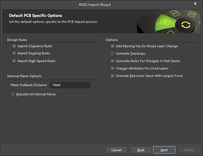
Default PCB Specific Optionsページは、PCBおよびPCBライブラリインポートプロセスに関するデフォルトオプションを設定するために使用されます。
Design Rulesの下にあるオプションを有効にして、インポートするデザインルールを指定してください(任意)。
テキストボックスに希望するPlane Pullback Distanceを指定します。すべての内部平面を再構築するには、Rebuild All Internal Planesチェックボックスを有効にします。
必要な追加オプションのチェックボックスを有効にしてください。
Current PCB and PCB Library Options

ウィザードのこのページを使用して出力プロジェクト構造を確認し、PADS PCBおよびPCBライブラリファイルをインポートする出力ディレクトリを指定します。Browse Folderアイコンを使用して、Project Output Directoryを検索して選択してください。
プロジェクト構造を編集するためのオプションにアクセスするには、Menuをクリックします:
-
Create Project – プロジェクトを追加するには、Create Projectダイアログを開くにはクリックしてください。

新しいプロジェクトを追加するには、Create Projectダイアログを使用してください。
-
Rename Project – 選択したプロジェクトの名前を変更するにはクリックしてください。このオプションは、*.PrjPcb fileが選択されている場合のみ利用可能です。
-
Remove Selected Projects – 選択したプロジェクトをPCB Projects構造から削除するには、クリックしてください。
-
Reset Structure to Default – PCB Projects構造をデフォルトにリセットするにはクリックしてください。
-
Add Designs to Project – プロジェクトにデザインを追加するにはクリックしてください。このオプションは*.PrjPcb fileが選択されているときのみ利用可能です。
-
Remove Selected Designs - 選択したデザインファイルを削除するにはクリックしてください。
PCB Projects領域で右クリックすると、Menuボタンをクリックしたときと同じメニューとサブメニューにアクセスできます。
Output PCB Projects

ウィザードのこのページを使用して出力プロジェクト構造を確認し、ファイルをインポートする出力ディレクトリを指定します。Browse Folderアイコンを使用してLibrary Output Directoryを検索して選択してください。
Closing the Wizard

PADSインポートウィザードが完了しました。ウィザードを閉じるにはFinishをクリックしてください。
Imported PADS Files:
ウィザードによって、ロジックファイル内の各PADS Logicシートに対して1つのAltium Designer回路図ドキュメントが生成されます。各翻訳されたロジックファイルは、自動的に作成されたAltium Designer PCBプロジェクトに*.PrjPCBファイル拡張子でグループ化されます。
インポートされたファイルは次のように翻訳されます:
ファイル変換
PADS Logicの回路図とPADS LayoutのPCBファイルは、インポートウィザードがそれらをAltium Designer形式のファイルに変換できるように、ASCIIファイルでなければなりません。
インポートされたPADSファイルは以下のように翻訳されます:
-
PADSレイアウト(*.ASC)ASCII PCBファイルは、Altium Designer PCBファイル(*.PcbDoc)に変換されます。
-
PADS Logic(*.TX)ASCII回路図ファイルは、Altium Designer回路図ファイルに変換されます。.TXTファイル内の各回路図ページは、単一のAltium Designer回路図ファイル(*.SchDoc)としてインポートされます。
-
PADSライブラリ(*.c)スケマティックシンボルファイルとPADS(*.p)パラメトリック部品データファイルは、Altium Designerスケマティックライブラリファイル(*.SchLib)に変換されます。
-
PADS PCBライブラリ(*.d) PCBデカールファイルは、Altium Designer PCBライブラリファイル(*.PcbLib)に変換されます。
-
翻訳されたPADS回路図とPCBファイルは自動的に1つのPCBプロジェクトにグループ化されず、回路図用のプロジェクトとPCB用の別のプロジェクトが作成されます。
► PADSで正しいASCIIファイルのセットを作成する方法について詳しく知りたい場合は、PADS移行ガイドをご覧ください。
► ウィザードがサポートしているPADS LogicおよびLayoutファイルのバージョンは何ですか?
ツールから別のツールへの移行は、最初のツールからインポートツールへのオブジェクトの変換の制限によって制約を受けます。すべてのオブジェクトタイプを変換できるわけではありません。Altiumは定期的にインポートウィザードの設計ファイルコンバーターを改善しているため、インポート中に問題が発生した場合は、Altium Designerが最新ビルドに更新されていることを確認してください。これにより、バージョンの互換性が向上し、より正確なインポートが可能になる場合があります。
PADS PCB ASCIIファイルのレイヤーマッピング
使用されるすべてのPADS PCBレイヤーは、インポートウィザードを使用する際にインポート前にAltium Designerレイヤーにマッピングする必要があります。設計ルールの自動作成、欠落しているビアやキープアウトの変換を制御するための追加オプションも提供されています。

インポートウィザードのレイヤーマッピングオプションを使用して、PADS PCBレイヤーをAltium Designerレイヤーに関連付けます。
PCB設計のインポート時にレイヤーがどのようにマッピングされるかについて注意すべき点です。レイヤーマッピングは、PADS PCBレイヤーの名前とAltium Designer PCBレイヤーの名前との間の単純なマッピングです。もちろん、提案されたデフォルトマッピングが与えられているだけなので、必要に応じて多くのマッピングを変更できます。このマッピングは、インポートウィザードによって各PCBのレイヤーマッピングを構築するために使用され、その後個別にカスタマイズすることができます。ここでの理論は、10個のPCB設計をインポートし、レイヤーAssembly 1をMechanical Layer 1にマッピングしたい場合、正しいレイヤーマッピングを得るために10個のPCB設計をそれぞれカスタマイズする必要がないというものです。
この方法でインポートする利点は、複数の設計をインポートする際にレイヤーマッピングのバッチ管理で多くの時間を節約できることです。この場合、デフォルトのレイヤーマッピングはあなたの設定に保存されます。これを使用するデメリットは、デフォルトのレイヤーマッピングが設計の異なる構造に対して常に賢明ではないため、後で手動で変更が必要になる場合があることです。あなたの状況に最適なものを決定する必要があります。
ネット名オプション
PADS Logicでは、ネットの接続性はネット名を使用して作成され、これはワイヤーのプロパティです。人間が割り当てたネット名を持たないワイヤーには、$$$13654のようなシステム生成のネット名が与えられます。Altium Designerは、人間が定義した名前を持たないネットを識別するために異なるアプローチを使用し、ネット内の1つのピンに基づいてシステムが割り当てた名前、例えばNetC15_1を作成します。
PADSの回路図をインポートする際、ウィザードにはDo not translate hidden net namesオプションが含まれています。これらのシステム生成の名前をインポートしないように、このオプションを有効にしておくことをお勧めします。代わりにAltium Designerは独自のシステム生成のネット識別子を使用します。
 隠されたネット名を変換しないようにしてください。これにより、Altium Designerがネット名を作成できるようになります。
インポートされたドキュメントの操作
PADS Logicでは、すべての設計作業はページ上で始まります。これは設計の論理的な作業領域であり、単一のPADS回路図設計ファイル内に複数の回路図ページが存在することがあります。
PADS Layoutでは、すべての設計作業はワークスペース、PCB設計の論理的な作業領域で始まります。各設計は単一の設計ファイル(*.PCBファイル)に保存されます。また、PCB設計の一部またはサブセットを設計内または別の設計で再利用するために保存できる物理設計再利用ファイル(*.REU)もありますが、これらは無視され、変換されません。
Altium Designerでは、論理設計領域はドキュメントから始まり、各ドキュメントにはハードドライブ上にファイルが保存されています。これは、Altium Designerの各回路図シート(ページ)が回路図ドキュメントファイルによって表されることを意味し、覚えておくべき重要な概念的な違いです。Altium Designerプロジェクトには、設計プロジェクトの性質に応じて、回路図およびPCB設計ドキュメントだけでなく、さまざまなタイプの複数のドキュメント(PDF、テキストファイル、スプレッドシートなどのネイティブでないファイルを含む)も含まれる場合があります。
オブジェクト変換の制限
-
PADS Logic: 個別のピン型コネクタはサポートされていません。これらは、すべてのピンが単一の回路図コンポーネントにあるブロックスタイルコネクタにPADSで変換するか、翻訳後にAltiumコネクタコンポーネントに変換する必要があります。
-
PADS Layout: 物理設計の再利用ブロックはサポートされていません。これらは、エクスポート/インポートの前にPADSで個々のパーツに分解する必要があります。PADSレイアウトでブロックを右クリックし、Break Reuseを選択してください。
パネル
Altium Designer環境の重要な特徴は、Projectsパネルなどのパネルです。Altium DesignerのProjectsパネルは、回路設計データに限定されず、PCB、すべてのライブラリ、出力ファイル、さらには非ネイティブファイル(PDF、テキストファイル、スプレッドシートなど)などの他のプロジェクト文書を含むことができます。Altium Designerのパネルは、アプリケーションの右下にある  ボタンを使用して表示できます
Altium Designerの機能について詳しくは、Altium Designerドキュメンテーションのセクションを参照してください。
回路図シンボルは部品です
PADS Layoutのエキスパートユーザーとして、パーツはPADS Layoutにおけるデザインの基本的な構成要素であることをご存知でしょう。パーツは、パーツタイプ、ロジックファミリー、ピン数、ゲート数、および信号ピンを持つことが定義されています。「コンポーネント」という用語は、パーツがPCBレイアウトデザイン内で物理オブジェクトとして配置されるときにのみ使用されます。
PADSレイアウト(PCB)では、部品は1つ以上の物理コンポーネントを表すことができます。PCB設計の部品は通常、ゲート、チップ、コネクタ、1つ以上の部品がパッケージになったオブジェクトに対応します。複数部品のパッケージは、1つ以上の部品から構成される物理オブジェクトです。
同じ用語をデザインの文脈によって使用するこの2つの定義は、コンポーネントという用語を使用する新しい環境では初めは混乱を引き起こすかもしれません。しかし、回路図記号はデザインのすべての段階における部品であり、PCBレイアウト部分だけではないという点を除けば、Altium Designerでの物事の動き方とそれほど違いはありません。
Altium Designerでは、論理シンボルはコンポーネントの基本的な出発点と見なされます。最小限では、ピンや実装に必要な任意のグラフィカルシンボルや代替表示オプションを追加できる回路図ライブラリ内の名前として定義できます。この柔軟性により、設計およびキャプチャプロセス中にコンポーネントをさまざまな方法で表現できます。これは、回路図上の論理シンボルとしてだけでなく、PCB上のフットプリントやシミュレーション用のSPICE定義としても可能です。
Altium Designerライブラリ
Altium Designerの統合ライブラリは、ソースシンボル、フットプリント、その他の情報(例:SPICEおよび他のモデルファイル)が1つのファイルにコンパイルされたものです。コンパイル中に、関係がどのように定義されているかを確認し、モデルとシンボル間の関係を検証し、これらを単一の統合ライブラリにまとめるためのチェックが行われます。このファイルはコンパイル後に直接編集することはできず、移植性とセキュリティを提供します。
PADSオブジェクト
|
Altium Designer オブジェクト
|
コメント
|
| デカール |
フットプリント
|
PCBに取り付けるために定義された形状のグラフィカルな表現です。これは2次元の表現のみであり、実際のコンポーネントとはかなり異なる場合があります。 |
部品
|
部品/コンポーネント
|
「部品」という用語は、Altium Designerの設計キャプチャ(回路図)プロセスの一部としてのみ使用されます。一度PCBファイルにフットプリントとして配置されると、設計者と値(コメント)が与えられ、コンポーネントになります。 |
線
|
線
|
グラフィカル情報に使用される原始的なオブジェクト。 |
CAEデカール
|
回路図シンボル
|
NORゲートのような回路部品の図解表現。 |
一般的に使用されるPADSライブラリ用語とそれに最も近いAltium Designerの相当語の表。
インポートされた回路の操作
短絡ネットのチェック
PADSではネット名はワイヤの属性ですが、Altium Designerではネットラベルオブジェクトをワイヤに触れるように配置することでネットに名前を付けます。PADSはワイヤの中点にユーザー定義のネット名を自動的に表示します。一般的ではありませんが、PADS回路図をインポートすると、Altium Designerのネットラベルが二つの別々のネットの交差点に位置する可能性があります。ネットラベルの接続点は左下隅(ホットスポットとも呼ばれます)であるため、Altium Designerではこれにより二つのネットが接続される場合があります。
インポートした回路図の視覚的な確認を常に行い、各ネットラベルの位置が適切であることを確認してください。ネットラベルを適切な位置に移動するためにクリックしてドラッグし、左下隅が名前を付けるネットのワイヤーに触れることを確認してください。
► 回路図で接続性を作成する方法についてもっと学びましょう。

MPSBネットラベルの位置により、ネットMPSBとネットGATEは短絡されています。SLNBネットラベルも2つのネットを短絡することに注意してください。
Altium Designerでは、Altキーを押しながらネット内の任意の要素を左クリックすることで、ネット内のすべての接続された要素を強調表示できます。
回路図の検証
Altium Designerは、回路図からコンポーネントおよび接続情報を自動的に抽出し、メモリ内に設計の包括的モデル(Unified Data Model)を構築します。このデータモデルは、その後、回路図の検証、基板への回路図の同期、部品表の作成、回路シミュレーションなどの分析タスクを実行するために使用されます。
回路図をPCBと同期する前に、接続の問題がないことを確認するために回路図を検証することが重要です。これを行うには、Project » Validate PCB Project <ProjectName> コマンドを実行します。検証結果はMessagesパネルに表示されます。
 Messagesパネルには検証の警告とエラーが詳細に表示されます。詳細セクションのエラーをダブルクリックすると、そのエラーにジャンプします。画像上にカーソルを置くと、エラーや警告のないプロジェクトが表示されます。
検証オプションはOptions for PCB Project <ProjectName>ダイアログで設定されます(Project » Project Optionsを選択)。エラーレポートタブと接続マトリックスタブの設定を確認してください。
► デザインプロジェクトの検証についてもっと学ぶ。
回路図からPCBへの同期
同じPCBデザインの回路図とボードの両方をインポートする場合、それらを単一のAltium Designerプロジェクトに組み合わせる必要があります。インポートウィザードは、インポートされた回路図がインポートされたボードと同じデザインの一部であるとは想定しません。デザイナーとして、これを確立する必要があります。ウィザードは、インポートされた回路図用に1つのAltium *.PrjPcbプロジェクトと、インポートされたPCB用に別の*.PrjPcbプロジェクトを作成します。各プロジェクトは、ソースPADSファイルと同じフォルダにある子フォルダに作成されます。回路図をボードと同期する前に、回路図とボードが同じプロジェクトに属している必要があります。
単一プロジェクトの作成
すべてのPADSファイルがインポートされたら、Altium Designerで両方のプロジェクトを閉じ、Windowsファイルエクスプローラーを使用して、回路図をPCBと同じフォルダに移動するか、PCBを回路図と同じフォルダに移動することをお勧めします。その後、完全なプロジェクトにする予定のプロジェクトを再度開き、Altium Designerのプロジェクトパネルでプロジェクト名を右クリックし、コンテキストメニューからAdd Existing to Projectコマンドを選択します。追加する必要のあるファイルを探して選択し、OpenボタンをクリックしてChoose Documentsダイアログを閉じます。
プロジェクトには、回路図とPCBの両方が含まれるようになります。
を追加します。") プロジェクトに回路図(または他のドキュメント)を追加します。
プロジェクトに回路図(または他のドキュメント)を追加します。
► プロジェクトドキュメントの管理についてもっと学ぶ。
プロジェクトオプションの設定
回路図シートとPCBはプロジェクトに属しています。プロジェクトオプションは Options for PCB Project <ProjectName> ダイアログ(Project » Project Options)で設定されます。
ダイアログの以下のタブが回路図からPCBへの同期中に使用されます:
-
クラス生成 - 自動ネットおよびコンポーネントクラス生成、およびルーム生成などのオプションを設定するために使用されます。コンポーネント配置ルームを特に使用したい場合を除き、Generate Roomsのチェックボックスを無効にすることをお勧めします。また、各回路図シート上のコンポーネントセットに対してComponent Classを作成することも望まないかもしれません。
-
コンパレータ - デザイン同期中にチェックするべき違いを定義します。通常、このタブのオプションを変更する必要はありません。
-
ECO生成 - 検出された違いに対してエンジニアリング変更命令を生成するかを定義します。通常、このタブのオプションを変更する必要はありません。
-
オプション - シート間の接続がどのように作成されるか(ネット識別スコープ)、ネットリストオプション、およびデフォルトのプロジェクト出力オプションなどのオプションを設定するために使用されます。ネット識別スコープが自動(プロジェクトの内容に基づく)に設定されていることを確認してください。自動設計コンパイラは、検出するネット識別子(ネットラベル、ポート、シートエントリ、デザイン階層など)に基づいて最適な設定を決定します。
回路図コンポーネントをPCBコンポーネントにリンクする
Altium Designerは、各回路図コンポーネントをPCBの対応物に接続し、両者に同じ一意の識別子(UID)を付与します。デザインがAltium Designerの回路図エディタで開始され、その後PCBエディタに転送されると、UIDは自動的に割り当てられます。回路図とPCBデザインがAltium Designerにインポートされている場合、このプロセスを自分で管理する必要があります。
各回路図コンポーネントをそのPCBコンポーネントにリンクするには、PCBを開き、PCBエディタでProject » Component Linksコマンドを選択して、Edit Component Linksダイアログを開きます。一致しない回路図とPCBコンポーネントは、ダイアログの左側の2つの列にリストされており、すでに一致するUIDが割り当てられているコンポーネントは、ダイアログの右側にリストされています。ダイアログの左下にある適切なオプションを有効にして、追加ペアを設計者、コメント、フットプリントによって自動的にチェックおよび一致させるAdd Pairs Matched Byボタンをクリックします。
一致しないコンポーネントがあり、それがなぜかわかる場合、たとえば回路図コンポーネントのコメントが PCB コンポーネントのコメントと一致しない場合は、コンポーネントが一致するようにオプションを調整します。また、それぞれの列で一致しない回路図コンポーネントと一致しない PCB コンポーネントを選択し、ダイアログの中央にある左から右のボタンをクリックすることで、手動でコンポーネントを一致させることもできます。
すべてのコンポーネントが一致したら、Perform Updateボタンをクリックします。そうすると、Altium DesignerはPCBコンポーネントUIDを回路図コンポーネントUIDに合わせて更新します。

各回路図コンポーネントは、Component Linksダイアログで割り当てられたUIDによって、PCBの対応物にリンクされています。
このプロセスの後、例として回路図上のロゴやPCB上のマウンティングホールのように、未一致のコンポーネントが残る可能性があります。これらは、Component Typeプロパティを適切な値、たとえばグラフィカルや機械的なものに設定することで、今後の比較から除外できます。
PCBに回路図を同期させる
回路図のコンポーネントがPCBの同等品と一致したら、完全な設計比較を実行できます。これを行うには、Altium Designerで回路図シートの1つをアクティブなドキュメントにし、次にDesign » Update PCB Document <PcbName>コマンドを選択します。Engineering Change Orderダイアログが開き、回路図と一致させるためにPCBに加える必要がある変更のリストが表示されます。
変更は一度の操作で適用する必要はありません。変更の数が多い場合や、確信が持てない変更がある場合は、特定のECOのみを有効にすることでプロセスを管理しやすくすることができます。チェックボックスを使用するか、右クリックのコンテキストメニューを使用して、1つ以上の変更を無効にします。

Engineering Change Orderダイアログで、有効な変更オーダーを検証し、実行します。
Engineering Change Orderダイアログのボタンを使用して、有効な変更を検証し、実行します。プロセスが完了したら、ダイアログを閉じるためにCloseボタンをクリックします。
► PCBとと回路図の同期についてもっと学ぶ。
回路図とPCBの間での作業
Altium Designerには、回路図とPCBの間で作業するのに役立つツールが含まれており、具体的には、Navigatorパネル、クロスプロービング、クロスセレクションがあります。Navigatorパネルは、全体の設計を通じてコンポーネント、そのピン、およびネットをブラウズするために使用できます(パネルの上部でFlattened Hierarchyを選択します)。
回路図とPCBの両方でオブジェクトを同時にナビゲートするには、パネルのエントリーをクリックしながらAltキーを押し続けてください。両方のエディターで同時にナビゲートしている場合は、作業スペースのビューを垂直または水平方向に分割したり、PCBを新しいウィンドウで開いたりすると便利です。ドキュメントタブを右クリックして、これらのコマンドにアクセスします。
 ナビゲーターパネルを使用して、設計内のコンポーネント、ピン、ネットを閲覧します。Altキーを押しながら、両方のエディタで同時に閲覧してください。
► 回路図と基板の間での作業についてもっと学ぶ。
PCB設計の確認
回路図とPCBが同期したら、最後の段階はPCBが正しくインポートされているかを確認することです。
PCBエディタのPCBパネルは、ボードデザイン内のオブジェクトをブラウズする優れた方法です。
ボードがロードされたら、デザインルールとポリゴンを確認し、デザインルールチェックを実行する必要があります。
デザインルールのレビュー
デザインルール(Design » Rules)を確認し、特に電気的クリアランスルール、プレーン接続およびクリアランスルールに注意を払ってください。Altium Designerでは、ルールはオブジェクトとは独立して存在します。適用対象となるオブジェクトは、ルールのスコープ(ルールのWhere the Object Matchesセクション)によって定義されます。

ルールの範囲 - ルールの適用範囲は、PADSレイアウトからのルール階層に取って代わります。範囲は、そのルールによって管理されるすべてのメンバーオブジェクトを定義するために構築するクエリです。これにより、完全な制御が可能になります。基準となる比較のために、PADSレイアウトのルール階層を見てみましょう。これらのルールは、リスト上での高い番号が低いものよりも優先されるという、事前定義されたリスト形式に依存しています:
-
デフォルト
-
クラス
-
ネット
-
グループ
-
ピンペア
-
デカール/コンポーネント
PADSレイアウトのルールスキーマでは、デフォルトルールはレベル1と見なされ、最低であり、デカールとコンポーネントのルールが最高を表します。条件付きレイヤールールは、優先順位の追加レベルに適用できます。例えば、条件付きレイヤールールを持つデフォルトは、単純なデフォルトルールよりも優先順位階層で高くなります。
Altium Designerでは、スコーピングにより、ルールの優先順位と対象オブジェクトへの適用方法を正確に決定できます。異なるオブジェクトを対象とする同じタイプの複数のルールを定義することもできます。カスタムクエリオプションも利用可能で、より複雑なクエリを自分で書くのに役立ちます。

PCB Rules and Constraint Editorダイアログで任意のルールにCustom Queryを選択すると、そのルールの特定のクエリを表示および編集できます。
設計ルールを使用したくないが、将来的に使用する可能性がある場合は、削除する代わりに単に無効にすることができます。関連するリストでルールのEnableオプションを切り替えます。
すべてのデフォルト設計ルールはAllの範囲を持ち、これはボード全体に適用されることを意味します。スコーピングに加えて、ユーザー定義の優先度設定もあります。ルールのスコーピングと優先度の組み合わせは非常に強力で、ボードの設計ルールを正確にターゲットにする前例のない制御レベルを提供します。
►設計ルールについてもっと学ぶ。
ポリゴンのレビュー
ポリゴンマネージャーでポリゴンプアをレビューします(Tools » Polygon Pours » Polygon Manager)。ポリゴンマネージャーは、レイヤーごとにクラスタリングされた設計内のすべてのポリゴンをリストします。
ポリゴンマネージャーを使用して:
設計ルールチェックを実行する
設計ルールをチェックする前に、以下を確認してください:
-
Rules are enabled - 設計ルールはPCBルールと制約エディタで個別に無効にすることができます。これはルールタイプレベルのツリーで行われ、個々のルールページではありません。
-
Rule priority is correct - 各タイプのルールセットは、優先順位の順にリストされており、必要に応じて順序を変更できます。
-
Display of Violations is configured - 違反はオーバーレイを使用して強調表示されるか、詳細表示、またはその両方で表示できます。これはPreferencesダイアログのDRC Violations Displayページで設定されます。必要な違反表示スタイルをすばやく有効にするために、チェックボックスリストで右クリックしてコンテキストメニューを表示します。
-
Rules are enabled for testing - デザインルールチェッカーダイアログを開いて、チェックしたいルールを有効にします(使用中のルールを切り替えるために右クリックコンテキストメニューを使用します)。
オンラインDRCは、設計編集イベントの後に自動的に実行されます。バッチDRCは、Design Rule Checkerダイアログのデザインルールチェックを実行ボタンをクリックすることで呼び出されます。
PCBエディタにはPCB Rules and Violationsパネルが含まれています。このパネルは、ルールを調べるだけでなく、ルール違反を閲覧する優れた方法を提供します。ルール違反を1回クリックすると、その違反にジャンプします(パネルの上部にある設定オプションに基づいて)、ダブルクリックすると、その違反に関するより詳細な情報が記載されたViolation Detailsダイアログが開きます。
 PCBルールと違反パネルを使用して、ルールと違反の両方を調べます。
PCBエディタのヒント
PCBエディタでの作業に役立つヒント:
-
Ctrl+WheelRoll - ズームインとズームアウト
-
WheelRoll - 上下にパンする
-
Shift+WheelRoll - 左にパンし、右にパンする
-
Ctrl+Shift+WheelRoll - ボードの層をステップスルーする
-
Right Mouse click and drag - ディスプレイウィンドウでボードをスライドさせる。
-
Shift+S - シングルレイヤーモードに切り替えるには、PreferencesダイアログのBoard Insight Displayページで利用可能なシングルレイヤーモードを構成してください。
-
Shift+C - 選択をクリアし、フィルターを表示する
-
2 or 3 - 2Dと3Dの表示モードを切り替える。
謝辞
PADS™はシーメンス・インダストリー・ソフトウェア社の登録商標です。
参照
以下はPADSデザインのインポートに関する他の記事や動画への参照です。メニュー項目、パネル、またはオブジェクトの上にカーソルを置いてF1を押すと、詳細情報を得ることもできます。

 AI で翻訳