Chinese - Translation is available for Altium Designer 23:
Go to the pageTranslating Siemens EDA® PADS™ software designs, including PADS Logic schematics, PADS Layout PCB files, and library files, can all be handled by Altium Designer's Import Wizard. The Import Wizard removes much of the headache normally found with design translation by analyzing the imported files and offering defaults and suggested settings for the project structure, layer mapping, PCB footprint naming, and more. The flexibility provided through the Wizard steps gives you control over the file translation settings before committing to the actual translation process.
To access PADS import capabilities in Altium Designer, the PADS feature must be enabled for your installation of Altium Designer. This feature is enabled in Altium Designer by default. It can be enabled/disabled after installation.
For more information about changing installed core functionality, refer to the Installing & Managing page (Altium Designer Develop, Altium Designer Agile, Altium Designer).
Importing PADS Files
The PADS design file importer is available through Altium Designer's Import Wizard (File » Import Wizard) by selecting the PADS ASCII Design and Library Files option on the Wizard's Select Type of Files to Import page. The Wizard provides options for nominating both schematic/pcb design files and library files, and also PADS to Altium Designer PCB import options.
 Select PADS ASCII Design and Library Files to import your PADS design files.
Import Wizard - PADS ASCII Design and Library Files
PADS ASCII Design and Library Files

The PADS designs imported by the Wizard are captured as documents in individual PCB projects that are created automatically after the translation in Altium Designer. Errors in the translation are reported in a log file with the extension *.LOG.
The Wizard only translates PADS ASCII versions 5.2 and above and does not read PADS binary files. If you only have binary PADS files, you will need to export these binary files into ASCII format from your PADS application, preferably in the ASCII 2005.2 format.
Importing PADS Designs

Click Add to choose which PADS design files to include in the process. You can delete a selected file by clicking Remove.
Importing PADS Libraries

Click Add to choose which PADS library files to include in the process. You can delete a selected file by clicking Remove.
Reporting Options

Use the Reporting Options page to set up general log reporting options.
Under General Settings, enable the desired options: Log All Errors, Log All Warnings, and Log All Events.
Enable Do not translate hidden net names if desired.
Default PCB Specific Options
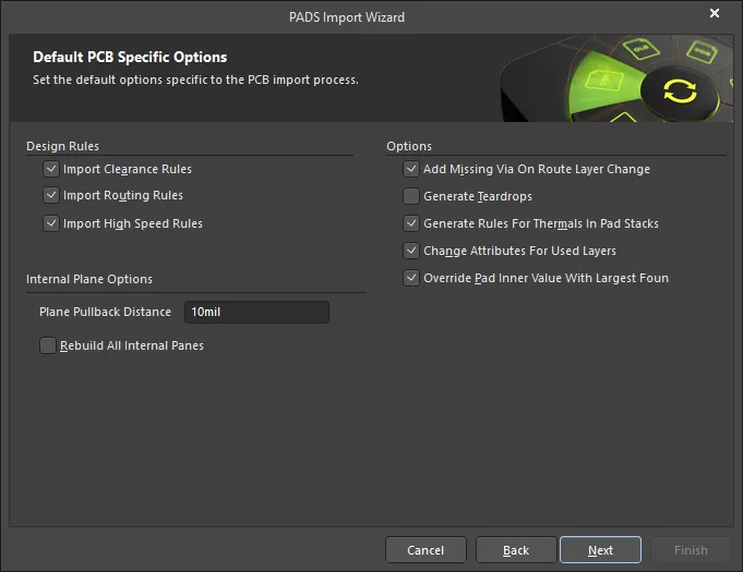
The Default PCB Specific Options page is used to set default options that pertain to both the PCB and PCB library import process.
Enable the options under Design Rules to specify which (if any) design rules to import.
Specify the desired Plane Pullback Distance in the textbox. Enable the checkbox to Rebuild All Internal Planes.
Enable the checkboxes of any desired additional Options.
Current PCB and PCB Library Options

Use this page of the Wizard to review the output project structure and specify the output directory in which to import PADS PCB and PCB library files. Use the Browse Folder icon to search for and choose the Project Output Directory.
Click Menu to access options to edit the project structure:
Right-clicking in the PCB Projects region gives access to the same menus and sub-menus as clicking the Menu button.
Output PCB Projects

Use this page of the Wizard to review the output project structure and specify the output directory in which to import the files. Use the Browse Folder icon to search for and choose the Library Output Directory.
Closing the Wizard

The PADS Import Wizard has completed. Click Finish to close the Wizard.
Imported PADS Files:
One Altium Designer schematic document is generated by the Wizard for each PADS Logic sheet within a logic file. Each translated logic file is grouped into automatically created Altium Designer PCB projects with an *.PrjPCB file extension.
Imported files translate as follows:
-
PADS ASCII Schematic Logic sheets within a Logic file with a
*.TXT extension translate to Altium Designer schematic files with an *.SchDoc file extension.
File Translation
Both the PADS Logic schematic and the PADS Layout PCB files must be ASCII files for the Import Wizard to be able to translate them to Altium Designer format files.
Imported PADS files translate as follows:
-
PADS Layout (*.ASC) ASCII PCB files translate to Altium Designer PCB files (*.PcbDoc).
-
PADS Logic (*.TXT) ASCII schematic files translate to Altium Designer schematic files. Each schematic page within a .TXT file will be imported as a single Altium Designer schematic file (*.SchDoc).
-
PADS library (*.c) schematic symbol files, combined with PADS (*.p) parametric parts data files will be translated into Altium Designer schematic library files (*.SchLib).
-
PADS PCB library (*.d) PCB decal files translate to Altium Designer PCB library files (*.PcbLib).
-
Translated PADS schematics and PCB files are not automatically grouped into one PCB project, a project is created for the schematics and another for the PCB.
► To learn more about creating the correct set of ASCII files in PADS, check out the PADS Migrating Guide.
► What versions of PADS Logic and Layout files are supported by the Wizard?
Migration from one tool to another is subject to the limitations of converting objects from the first tool to the importing tool. It is sometimes not possible to translate all object types. Altium regularly improves the Import Wizard's design file converters, so if difficulty is encountered during an import, ensure that Altium Designer has been updated to the most current build. This may result in better version compatibility and more accurate imports.
Layer Mapping for PADS PCB ASCII Files
All used PADS PCB layers must be mapped to an Altium Designer layer prior to import when using the Import Wizard. There are additional options provided to control the automatic creation of design rules, missing vias and keep-out conversions as well.

Use the layer mapping options in the Import Wizard to associate PADS PCB layers to Altium Designer layers.
It should be noted about how the layers are mapped on import for PCB designs. Layer Mapping is simply a mapping between the names of the PADS PCB layers and Altium Designer PCB layers. Of course, you can change as many mappings as you want as only suggested default mappings are given. This mapping is used by the Import Wizard to build the layer mapping for each PCB that can then be individually customized. The rationale here is that should you wish to import ten PCB designs and you want to map the layer Assembly 1 to Mechanical Layer 1, you would not have to customize each of the ten PCB designs in order to get the right layer mapping.
The advantage to importing in this manner is that batch management of layer mapping can save a lot of time when importing multiple designs. In this instance, the default layer mapping will be saved to your Preferences. The disadvantage to using this is that Default Layer Mapping is not always intelligent with differing structures in designs, and so some manual changes may be needed afterwards. You'll need to decide what is best for your situation.
Net Name Options
In PADS Logic, net connectivity is made using net names, which is a property of the wire. Wires that do not have a human-assigned net name are given a system-generated net name, such as $$$13654. Altium Designer uses a different approach for identifying nets that do not have a human-defined name, creating a system-assigned name based on one pin in the net, for example NetC15_1.
During import of a PADS schematic the Wizard includes the option, Do not translate hidden net names. It is recommended to keep this option enabled so that these system-generated names are not imported, instead Altium Designer will use its own system-generated net identifiers.
 Leave the Do not translate hidden net names, this allows Altium Designer to create net names instead.
Working with Imported Documents
In PADS Logic, all design work begins on the page, which is the logical working area of the design, and there can be multiple schematic pages within a single PADS schematic design file.
In PADS Layout, all design work begins on the workspace, the logical working area of the PCB design. Each design is saved to a single design file (*.PCB file). There are also physical design reuse files (*.REU) which allow you to preserve a portion or subset of a PCB design for reuse within the design or in another design - these are ignored and not translated.
In Altium Designer, the logical design area begins with a document, and for each document, there is a file stored on the hard drive. This means that each Altium Designer schematic sheet (page) is represented by a schematic document file, an important conceptual difference to remember. Note that an Altium Designer project can also include multiple documents of varying types (beyond just schematic and PCB design documents), depending on the nature of the design project.
Object Translation Limitations
-
PADS Logic: Individual pin-type connectors are not supported. These must either be: converted to block style connectors in PADS, so that all pins are in a single schematic component, or, those in-type connectors must be converted to an Altium connector component, post-translation.
-
PADS Layout: Physical Design Resuse blocks are not supported. These must be broken down into individual parts in PADS, prior to export/import. Right-click on the block in PADS Layout and select Break Reuse to do this.
Panels
A key feature of the Altium Designer environment are the panels, such as the Projects panel. In Altium Designer the Projects panel is not limited to schematic design data, it can include the PCB, all libraries, output files, as well as other project documents, such as non-native files (PDFs, text files, spreadsheets, etc.). Altium Designer panels can be displayed using the  button, located at the bottom right of the application.
The Schematic Symbol is the Part
As an expert PADS Layout user, you'll know that parts form the basic building blocks of design in PADS Layout. Parts are defined as having a part type, a logic family, number of pins, number of gates, and signal pins. The term component is only used when the part becomes placed as a physical object in the PCB layout design.
In PADS Layout (PCB), a part can represent one or more physical components. Parts in PCB designs usually correspond to physical objects: gates, chips, connectors, objects that come in packages of one of more parts. Multiple-part packages are physical objects that are comprised of one or more parts.
These two definitions that use the same term depending on the context of design may initially cause some confusion in the new environment which uses the term component. But it is not unlike how things work in Altium Designer except that the schematic symbol is effectively the part for all phases of design, and not just the PCB Layout portion of it.
In Altium Designer, the logical symbol is assumed to be the essential starting point of a component. It can be initially defined at minimum as a name in a schematic library to which pins and any graphical symbols or alternative display options needed for implementation may be added. This flexibility allows a component to be represented in different ways during the design and capture process. This may not only be as a logical symbol on the schematic, but also be a footprint on the PCB or even as a SPICE definition for simulation.
Altium Designer Libraries
An integrated library in Altium Designer is one where the source symbol, footprint, and all other information (e.g. SPICE and other model files) are compiled into a single file. During compilation checks are made to see how relationships are defined, to validate the relationship between the models and the symbols and to bundle them into a single integrated library. This file can not be directly edited after compilation, offering portability and security.
PADS Object
|
Altium Designer Object
|
Comments
|
Decal
|
Footprint
|
Graphical representation of the shape defined for the component to mount onto the PCB. This is 2-dimensional representation only, and can be quite different from the actual component itself
|
Part
|
Part/Component
|
The term Part is used only as part of the design capture (schematic) process in Altium Designer. Once placed as a footprint into a PCB file, it is given a designator and value (comment) and becomes a component.
|
Lines
|
Lines
|
Primitive object used for graphical information.
|
CAE Decal
|
Schematic symbol
|
The graphical representation of a schematic part, such as a NOR gate.
|
A table of the more commonly-used PADS Library terms and their closest respective Altium Designer equivalents.
Working with the Imported Schematic
Check for Net Shorts
In PADS, the net name is an attribute of the wire, whereas in Altium Designer the net is named by placing a Net Label object so that it touches the wire. PADS automatically displays a human-defined net name at the midpoint of the wire. Although it is not common, it is possible that when the PADS schematic is imported, the Altium Designer Net Label will be located right at the cross-over point of two separate nets. Because the connective point on a Net Label is the bottom left corner (also referred to as the hotspot), in Altium Designer this can result in those two nets being connected together.
Always perform a visual check of the imported schematic and confirm that the location of each Net Label is appropriate. Click and drag to move the Net Label to a suitable location, ensuring that the bottom left corner touches the wire of the net being named.
► Learn more about Creating Connectivity in your Schematics.
In Altium Designer you can highlight all connected elements in a net by holding the Alt key and left mouse clicking on any element in that net.
Validating the Schematic
Altium Designer automatically extracts component and connective information from the schematic and builds a comprehensive model of the design in memory, referred to as the Unified Data Model. This data model is then used for tasks such as: validating the schematic, synchronizing the schematic to the board, creating the BOM, and performing analysis tasks such as circuit simulation.
Before proceeding to synchronize the schematic with the PCB, it is important to Validate the schematic to confirm that there are no connective issues. To do this, run the Project » Validate PCB Project <ProjectName> command. Validation results are displayed in the Messages panel.
Validation options are configured in the Options for PCB Project <ProjectName> dialog (select Project » Project Options). Review the settings on the Error Reporting and Connection Matrix tabs.
► Learn more about Validating Your Design Project.
Schematic to PCB Synchronization
If you are importing both the schematics and the board of the same PCB design, you will need to combine them in a single Altium Designer project. The Import Wizard does not assume that imported schematics are part of the same design as an imported board, as the designer you will need to establish this. The Wizard will create one Altium *.PrjPcb project for the imported schematic(s), and another *.PrjPcb project for the imported PCB, each project is created in a child folder located in the same folder as the source PADS files. Before the schematic can be synchronized with the board, the schematic(s) and the board must belong to the same project.
Creating a Single Project
Once all of the PADS files have been imported, it is recommended that you close both of the projects in Altium Designer, and use the Windows File Explorer to either move the schematics into the same folder as the PCB, or move the PCB into the same folder as the schematics. Then re-open the project that you plan to become the complete project, right-click on the project name in the Altium Designer Projects panel and select the Add Existing to Project command from the context menu. Locate and select the files that need to be added and click the Open button to close the Choose Documents dialog.
The project will now include both the schematics and the PCB.
► Learn more about Managing Project Documents.
Configuring the Project Options
The schematic sheets and the PCB belong to the project. The project options are configured in the Options for PCB Project <ProjectName> dialog (Project » Project Options).
The following tabs of the dialog are used during schematic to PCB synchronization:
-
Class Generation - used to configure options such as automatic net and component class generation, and room generation. Unless you specifically want to use component placement rooms, it is recommended that you disable the Generate Rooms checkboxes. You also may not want to create a Component Class for the set of components on each schematic sheet.
-
Comparator - defines what differences should be checked for, during design synchronization. Typically the options on this tab do not need to be changed.
-
ECO Generation - defines which detected differences should have engineering change orders generated. Typically the options on this tab do not need to be changed.
-
Options - used to configure options such as how the sheet-to-sheet connectivity is created (Net Identifier Scope), netlisting options, and default project output options. Confirm that the Net Identifier Scope is set to Automatic (Based on project contents). The automatic design compiler will determine the best setting, based on what net identifiers it detects (Net Labels, Ports, Sheet Entries, design hierarchy, etc).
Linking the Schematic Components to the PCB Components
Altium Designer connects each schematic component to its PCB counterpart by issuing them both the same unique identifier (UID). When the design is started in Altium Designer's schematic editor and then transferred to the PCB editor, the UIDs are assigned automatically. If the schematic and PCB designs have been imported into Altium Designer, you will need to manage this process yourself.
To link each schematic component to its PCB component, open the PCB and select the Project » Component Links command in the PCB editor to open the Edit Component Links dialog. Unmatched schematic and PCB components are listed in the two columns on the left side of the dialog, components that already have matching UIDs assigned are listed on the right side of the dialog. Enable the appropriate options down the bottom left of the dialog and click the Add Pairs Matched By button to automatically check and match components by Designator, Comment and Footprint.
If there are components that do not match and you understand why - perhaps the component Comment in the schematic component does not match the Comment in the PCB component - adjust the options as required to get the components to match. You can also manually match components by selecting the unmatched schematic component and the unmatched PCB component in the respective columns, and clicking the left to right button in the middle of the dialog.
Once all of the components are matched, click the Perform Update button. When you do, Altium Designer will update the PCB component UIDs to match the schematic component UIDs.
There may be components that remain unmatched after this process, for example a logo on the schematic, or a mounting hole on the PCB. These can be excluded from future comparisons by setting their Component Type property to a suitable value, such as Graphical or Mechanical.
Synchronizing the Schematic to the PCB
Once the schematic components have been matched to their PCB equivalent, a full design comparison can be performed. To do this, make one of the schematic sheets the active document in Altium Designer, then select the Design » Update PCB Document <PcbName> command. The Engineering Change Order dialog will open, displaying a list of changes that must be made to the PCB to get it to match the schematic.
The changes do not have to be applied in a single operation, if there is a large number of changes or changes you are not sure about, it can be easier to manage the process by only enabling specific ECOs. Use the checkboxes, or the right-click context menu to disable one or more changes.
-
If there is an unmatched PCB component that has not had its Component Type changed to Graphical or Mechanical, there will be an ECO to remove it from the board. Disable this ECO, then when the ECO process is complete change the Component Type.
-
If there are ECOs to remove nets, it is recommended that you disable these and compare the schematic to the PCB to ensure that the imported design is correct.
Use the buttons in the Engineering Change Order dialog to Validate and Execute the enabled changes. When the process is complete, click the Close button to close the dialog.
► Learn more about Schematic to PCB Synchronization.
Working Between the Schematic and the PCB
Altium Designer includes tools to help you work between the schematic and the PCB, including: the Navigator panel, Cross Probing, and Cross Selection. The Navigator panel can be used to browse the components, their pins, and the nets across the entire design (select Flattened Hierarchy at the top of the panel).
To navigate to an object in both the schematic and the PCB at the same time, hold the Alt key as you click on an entry in the panel. If you are navigating in both editors simultaneously, it helps to either split the workspace view vertically or horizontally, or open the PCB in a new window. Right click on a document tab to access these commands.
► Learn more about Working Between the Schematic and the Board.
Verifying the PCB Design
Once the schematic and the PCB have been synchronized, the last stage is to verify that the PCB has been imported correctly.
The PCB panel in the PCB editor is an excellent way of browsing objects in the board design.
Once the board has loaded, you should review the design rules and the polygons, and perform a Design Rule Check.
Review the Design Rules
Review the Design Rules (Design » Rules), paying particularly attention to the Electrical Clearance rules, and the Plane Connect and Clearance rules. In Altium Designer, the rules exist independently from the objects. The object(s) that they apply to (target) is defined by their rule scope (the Where the Object Matches section of the rule).
Rules Scope - the extent of a rule's application - replaces the Rules Hierarchy from PADS Layout. A scope is effectively a query that you build to define all the member objects that are governed by that rule, giving you full control. For the sake of a baseline comparison, let's review the Rules Hierarchy of PADS Layout. These rules rely on a pre-defined list format where higher numbers on the list have precedence over those that are lower:
-
Default
-
Class
-
Net
-
Group
-
Pin Pair
-
Decal/Component
In the PADS Layout rules schema, Default rules are considered level 1 and are the lowest while Decal and Component rules represent the highest. Conditional layer rules can be applied for an additional level of precedence. For example, a Default with a conditional layer rule would be higher in the precedence hierarchy than a simple Default rule.
In Altium Designer, scoping allows you to decide exactly what a rule's precedence will be and how it will be applied to target objects through a query. You can even define multiple rules of the same type, but each targeting different objects. Custom Query options are also available to help you write your own, more complex queries.
If you do not want to use a design rule, but may want to use it in the future, rather than delete it you can simply disable it. Toggle the corresponding Enable option for the rule in the relevant list.
All default design rules have a scope of All, meaning that they apply to the whole board. In addition to scoping, there is also a user-defined priority setting. The combination of rule scoping and priority is very powerful and gives an unprecedented level of control that allows you to precisely target the design rules for your board.
► Learn more about Design Rules.
Review the Polygons
Review the Polygon Pours in the Polygon Pour Manager (Tools » Polygon Pours » Polygon Manager). The Polygon Manager lists all polygons in the design, clustered by layer.
Use the Polygon Manager to:
-
Change the pour order (important if there is a small polygon enclosed by a larger polygon).
-
Repour one or more polygons (the upper list supports standard Windows multi-select techniques).
-
Edit the properties of any polygon.
Perform a Design Rule Check
Before you check the design rules, confirm that the:
-
Rules are enabled - Design rules can be individually disabled in the PCB Rules and Constraints Editor. This is done at the rule-type level of the tree, not on the individual rule page.
-
Rule priority is correct - The set of each type of rule is listed in their order of priority, the order can be changed if required.
-
Display of Violations is configured - Violations can be highlighted using an overlay, or display detail, or both. This is configured in the DRC Violations Display page of the Preferences dialog. Right-click in the checkbox list to display a context menu where you can quickly enable the required Violation Display Style(s).
-
Rules are enabled for testing - Open the Design Rule Checker dialog to enable the rules you want to check (use the right-click context menu to toggle used rules on).
Online DRC is automatically run after any design edit event. Batch DRC is invoked by clicking the Run Design Rule Check button in the Design Rule Checker dialog.
The PCB editor includes a PCB Rules and Violations panel. The panel provides an excellent method of examining the rules, as well as browsing rule violations. Click once on a rule violation to jump to that violation (based on the configuration options at the top of the panel), double-click to open the Violation Details dialog, for more detailed information about that violation.
PCB Editor Tips
Useful tips for working in the PCB editor:
-
Ctrl+WheelRoll - zoom in and out
-
WheelRoll - pan up and down
-
Shift+WheelRoll - pan left and right
-
Ctrl+Shift+WheelRoll - step through the layers in the board
-
Right Mouse click and drag - slide the board around in the display window.
-
Shift+S - to cycle through to single layer mode, configure the available Single Layer Modes in the Board Insight Display page of the Preferences dialog.
-
Shift+C - clear selections and display filters
-
2 or 3 - switch between 2D and 3D display modes.
Acknowledgments
PADS™ is a registered trademark of Siemens Industry Software Inc.
See Also
Below are references to other articles and videos about importing a PADS design. You can also press F1 when the cursor is over a menu entry, a panel, or an object, for more information.
