
Работа с контактными площадками и переходными отверстиями
Сводка по контактным площадкам и переходным отверстиям

 Контактные площадки используются как для механического крепления, так и для электрического соединения с выводами компонентов
Контактная площадка — это примитивный объект проектирования. Площадки используются для крепления компонента к плате и для создания точек межсоединения от выводов компонента к трассировке на плате. Площадки могут существовать на одном слое, например как площадка для поверхностного монтажа (SMD), либо могут быть трехмерными металлизированными сквозными площадками с цилиндрическим телом в плоскости Z (по вертикали) и плоской областью на каждом (горизонтальном) медном слое. Цилиндрическое тело площадки формируется при сверлении платы и металлизации отверстий в процессе изготовления. В плоскостях X и Y площадки могут иметь круглую, прямоугольную, восьмиугольную, скругленно-прямоугольную, прямоугольную со скошенными углами или пользовательскую форму. Площадки могут использоваться по отдельности как свободные площадки в проекте, но чаще они применяются в редакторе библиотек PCB, где объединяются с другими примитивами в посадочные места компонентов.
 с нижним слоем (синий), а также подключенное к одной внутренней плоскости питания (зеленый).")
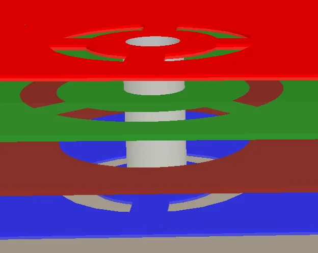
Переходное отверстие, проходящее и соединяющее верхний слой (красный) с нижним слоем (синий), а также подключенное к одной внутренней плоскости питания (зеленый).
Переходное отверстие — это примитивный объект проектирования. Переходные отверстия используются для формирования вертикального электрического соединения между двумя или более электрическими слоями PCB. Переходные отверстия являются трехмерными объектами и имеют цилиндрическое тело в плоскости Z (по вертикали) с плоским кольцом на каждом (горизонтальном) медном слое. Цилиндрическое тело переходного отверстия формируется при сверлении платы и металлизации отверстий в процессе изготовления. В плоскостях X и Y переходные отверстия имеют круглую форму, как и круглые площадки. Ключевое отличие переходного отверстия от площадки состоит в том, что, помимо возможности проходить через все слои платы (от верхнего до нижнего), переходное отверстие также может соединять поверхностный слой с внутренним слоем или два внутренних слоя между собой.
Непосредственное размещение площадок и переходных отверстий
Площадки и переходные отверстия доступны для размещения как в редакторе PCB, так и в редакторе посадочных мест PCB. Переходные отверстия обычно размещаются автоматически в процессе интерактивной или автоматической трассировки, но при необходимости их можно размещать вручную. Переходные отверстия, размещенные вручную, называются «свободными». После запуска команды размещения площадки (Place » Pad) или переходного отверстия (Place » Via) курсор изменится на перекрестие, и вы перейдете в режим размещения.
- Установите курсор в нужную позицию, затем щелкните мышью или нажмите Enter, чтобы разместить площадку/переходное отверстие.
- Продолжайте размещать следующие площадки/переходные отверстия либо щелкните правой кнопкой мыши или нажмите Esc, чтобы выйти из режима размещения.
Во время размещения нажмите клавишу Alt, чтобы ограничить направление перемещения по горизонтальной или вертикальной оси в зависимости от первоначального направления движения.
Графическое редактирование
Свойства площадок и переходных отверстий нельзя изменять графически, за исключением их положения.
- Чтобы переместить свободную площадку вместе с подключенными дорожками, щелкните по площадке, удерживайте кнопку мыши и перемещайте ее. Подключенная трассировка останется присоединенной к площадке во время перемещения. Обратите внимание, что площадка не будет перемещаться, если она принадлежит компоненту.
- Чтобы переместить свободную площадку без перемещения подключенных дорожек в редакторе PCB или PCB Library Editor, выберите команду Edit » Move » Move, затем щелкните по площадке, удерживайте кнопку мыши и перемещайте ее.
Неграфическое редактирование через панель Properties
Этот метод редактирования использует соответствующий режим панели Properties для изменения свойств объекта Pad/Via.
Pad Properties

Режим Pad панели Properties
Информация о цепи
В этой области отображается информация о цепи, к которой принадлежит площадка, а также о дифференциальной паре и/или xSignal, если данная цепь входит в их состав. Там, где это применимо, также отображается информация о классе. Значения Delay и Length также приводятся.
Подробнее об информации о цепях см. на странице Методы размещения и редактирования в PCB.
Свойства
-
Component – это поле отображается только в редакторе PCB, когда выбранная площадка является составной частью PCB-компонента, и показывает позиционное обозначение родительского PCB-компонента. Выберите кликабельную ссылку Component, чтобы открыть режим Component панели Properties для родительского компонента.
-
Designator – это поле отображает текущее обозначение площадки. Если площадка является частью компонента, обозначение обычно соответствует номеру вывода компонента. Свободные площадки могут содержать обозначение, либо это поле можно оставить пустым. Если обозначение начинается или заканчивается цифрой, число будет автоматически увеличиваться при последовательном размещении серии площадок. Измените значение в этом поле, чтобы изменить обозначение площадки.
-
Layer – выберите слой, которому назначена площадка. Выберите Multi-Layer, чтобы определить металлизированную сквозную площадку.
-
Net – используется для выбора цепи для площадки. Все цепи активного проекта платы будут перечислены в раскрывающемся списке. Выберите No Net , чтобы указать, что площадка не подключена ни к одной цепи. Свойство Net примитива используется модулем проверки правил проектирования (Design Rule Checker) для определения, корректно ли размещен объект PCB. Кроме того, можно щелкнуть значок Assign Net (
 ), чтобы выбрать объект в рабочей области проекта — цепь этого объекта будет назначена выбранной площадке(ам).
-
Electrical Type – в этом поле отображается текущий электрический статус площадки. Этот статус имеет значение только для площадок компонента и задает характеристики линии передачи для этих площадок. Площадки могут быть обозначены как Load, Source или Terminator. Параметры Source и Terminator используются, когда для цепи требуется одна из топологий трассировки Daisy chain. Щелкните поле, чтобы изменить электрический тип из раскрывающегося списка.
-
Propagation Delay – в этом поле указан delay распространения сигнала, то есть время, за которое фронт сигнала проходит путь от передатчика к приемнику.
-
Pin Package Length – длина корпуса вывода (Pin Package Length) автоматически включается в расчеты Signal Length, отображаемые на панели PCB. Установите панель PCB в режим Nets, чтобы просмотреть (или отредактировать) значение Pin/Pkg Length для выводов в выбранной цепи.
-
Jumper – это поле задает площадке идентификационный номер перемычечного соединения (в диапазоне от 1 до 1000), когда на PCB используется перемычка. Перемычечное соединение использует провод для физического соединения площадок на PCB и не использует дорожки или электрические объекты на плате. Значение Jumper указывает программе, какие площадки следует считать «соединенными». Перемычечное соединение может быть создано только между площадками в пределах посадочного места компонента. Используемые площадки должны иметь одинаковое значение Jumper и также принадлежать одной и той же цепи. В PCB Editor перемычечное соединение отображается как изогнутая линия соединения. Используйте стрелки прокрутки или введите нужный идентификационный номер перемычечного соединения напрямую.
-
Template – отображает текущий шаблон площадки. Используйте раскрывающийся список, чтобы выбрать другой шаблон. Если имеется связанная библиотека Library, будет показана именно она. Нажмите кнопку
 , чтобы отвязать шаблон от связанной библиотеки шаблонов Pad/Via.
-
(X/Y)
-
X (первое поле) – это поле показывает текущую координату X центра площадки относительно текущего начала координат. Измените значение в поле, чтобы изменить положение площадки относительно текущего начала координат. Значение можно вводить как в метрических, так и в дюймовых единицах; указывайте единицы измерения при вводе значения, если они отличаются от текущих единиц по умолчанию. Единицы по умолчанию (метрические или дюймовые) определяются параметром Units в области Other панели Properties в режиме Board (доступен, когда в рабочей области не выбраны объекты) и используются, если единица измерения не указана.
-
Y (второе поле) – это поле показывает текущую координату Y центра площадки относительно текущего начала координат. Измените значение в поле, чтобы изменить положение площадки относительно текущего начала координат. Значение можно вводить как в метрических, так и в дюймовых единицах; указывайте единицы измерения при вводе значения, если они отличаются от текущих единиц по умолчанию. Единицы по умолчанию (метрические или дюймовые) определяются параметром Units в области Other панели Properties в режиме Board (доступен, когда в рабочей области не выбраны объекты) и используются, если единица измерения не указана.
-
-
Rotation – угол поворота площадки (в градусах), измеряемый против часовой стрелки от нуля (то есть от 3 o'clock по горизонтали). Измените значение в этом поле, чтобы изменить поворот площадки. Минимальное угловое разрешение составляет 0,001°.
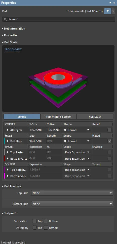
Pad Stack
-
Simple / Top-Middle-Bottom / Full Stack – выберите нужный режим стека площадки для металлизированной сквозной площадки (то есть когда Multi-Layer выбран в качестве Layer площадки). Для других слоев применяются параметры режима Simple.
-
Simple – выберите этот вариант, чтобы использовать простую многослойную площадку. Можно определить атрибуты формы площадки, общие для всех сигнальных медных слоев этой площадки.
-
Top-Middle-Bottom – выберите этот вариант, чтобы использовать многослойную площадку Top-Middle-Bottom. Можно определить размеры X и Y, а также атрибуты формы для верхнего, среднего и нижнего сигнальных медных слоев этой площадки.
-
Full Stack – выберите этот вариант, чтобы использовать многослойную площадку Full Stack. Можно определить размеры X и Y, а также атрибуты формы для всех сигнальных медных слоев этой площадки.
-
-
Copper – разверните сворачиваемые области или используйте таблицу, чтобы задать атрибуты площадки на сигнальных медных слоях. Набор доступных медных слоев зависит от слоя, на котором размещена площадка, и выбранного режима стека площадки.

- Shape– выберите форму контактной площадки. Стандартными формами площадок (Round, Rectangular, Octagonal, Rounded Rectangle, Chamfered Rectangle и Donut) можно управлять, изменяя параметры X и Y, чтобы получать асимметричные формы площадок. Выберите Custom Shape, чтобы задать площадку нестандартной формы (подробнее).
-
Edit Shape– нажмите, чтобы интерактивно редактировать область площадки пользовательской формы в рабочем пространстве проекта. Эта кнопка доступна, только если в качестве Shape выбрано Custom Shape.
-
(X/Y)– задайте размер площадки по X (горизонтали) и Y (вертикали). Размеры X и Y можно задавать независимо, чтобы определять асимметричные формы площадок. Значение можно вводить как в метрических, так и в имперских единицах; указывайте единицы измерения при вводе значения, если они отличаются от текущих единиц по умолчанию. Единицы по умолчанию (метрические или имперские) определяются параметром Units в области Other панели Properties в режиме Board (доступен, когда в рабочем пространстве не выбраны никакие объекты) и используются, если единица измерения не указана. Этот параметр доступен, только если в качестве Shape выбрано Rounded Rectangle или Chamfered Rectangle .
-
Corner Radius– введите абсолютное значение радиуса/фаски угла площадки. Значение должно быть меньше или равно половине самой короткой стороны площадки. Справа от поля будет показано вычисленное значение в процентах (процент от половины самой короткой стороны площадки). Введите значение с символом
%, чтобы задать радиус/фаску как процент от половины самой короткой стороны площадки, где100%полностью скругляет самую короткую сторону (в этом случае справа от поля будет показано вычисленное абсолютное значение). Этот параметр доступен только если для Shape площадки на соответствующем медном слое выбрано Rounded Rectangle или Chamfered Rectangle. -
Upper Left, Upper Right, Lower Left, Lower Right – включите, чтобы углы формы площадки были скруглены/срезаны фаской. Эти параметры доступны только если для Shape площадки на соответствующем медном слое выбрано Rounded Rectangle или Chamfered Rectangle.
-
Outer Diameter– введите внешний диаметр площадки. Этот параметр доступен, только если для Shape площадки на соответствующем медном слое выбрано Donut.
-
Width– введите ширину площадки. Этот параметр доступен, только если для Shape площадки на соответствующем медном слое выбрано Donut.
-
Thermal Relief– включите, чтобы настроить термобарьер для площадки, переопределив применимое правило Polygon Connect Style. После установки флажка щелкните ссылку, чтобы открыть диалоговое окно Polygon Connect Style, где можно изменить параметры термобарьера по мере необходимости. Нажмите кнопку Edit Points, чтобы вручную задать точки подключения лучей термобарьера. Подробнее см. Определение пользовательских термобарьеров.
-
Center Offset (X/Y) (только для SMD-площадки, то есть когда в качестве Layer площадки выбран слой, отличный от Multi-Layer) – введите значение смещения контактной области площадки относительно ее центра.
-
Hole– разверните сворачиваемый раздел или используйте таблицу, чтобы задать атрибуты отверстия площадки. Параметры отверстия доступны только для металлизированной сквозной площадки (то есть когда в качестве Layer площадки выбрано Multi-Layer).

-
Shape– выберите требуемую форму отверстия.
- Round– задает круглую форму отверстия для размера отверстия площадки. Для каждого типа отверстий, а также для металлизированных и неметаллизированных отверстий создаются отдельные файлы сверловки (формат NC Drill Excellon 2). Для этих типов может быть до шести различных файлов сверловки.
- Rectangular– задает для этой площадки прямоугольное (пробивное) отверстие. Прямоугольные отверстия могут быть металлизированными или неметаллизированными. Для каждого типа отверстий, а также для металлизированных и неметаллизированных отверстий создаются отдельные файлы сверловки (формат NC Drill Excellon 2). Для этих типов может быть до шести различных файлов сверловки.
- Slot– задает для этой площадки продолговатое отверстие с закругленными концами. Продолговатые отверстия могут быть металлизированными или неметаллизированными. Для каждого типа отверстий, а также для металлизированных и неметаллизированных отверстий создаются отдельные файлы сверловки (формат NC Drill Excellon 2). Для этих типов может быть до шести различных файлов сверловки.
- Size– в этом поле отображается текущий размер отверстия площадки. Значение задает диаметр круглого отверстия (или ширину прямоугольного или продолговатого отверстия) в mil или мм, которое будет сформировано в площадке при изготовлении. Для SMD-площадок или краевых разъемов это значение должно быть равно нулю. Размер отверстия можно задавать в диапазоне от 0 до 1000 mil; он может быть больше самой площадки для определения механических отверстий (без меди), но не может быть больше Length для отверстия Rectangular или Slot. Измените значение в этом поле, чтобы изменить размер отверстия площадки. Значение можно вводить как в метрических, так и в имперских единицах; указывайте единицы измерения при вводе значения, если они отличаются от текущих единиц по умолчанию. Единицы по умолчанию (метрические или имперские) определяются параметром Units в области Other панели Properties в режиме Board (доступен, когда в рабочем пространстве не выбраны никакие объекты) и используются, если единица измерения не указана.
-
Tolerance– задание допусков отверстия помогает определить посадки и предельные размеры вашей платы. Укажите минимальный (-) и максимальный (+) допуски для отверстия.
-
Length– отображает длину отверстия в площадке, когда Shape отверстия задан как Rectangular или Slot. Значение задает длину в мм или mil, которая будет выполнена NC-обработкой в площадке при изготовлении. Размер отверстия можно задавать в диапазоне от 0 до 1000 mil; он может быть больше самой площадки для определения механических отверстий (без меди), но не может быть меньше Size отверстия Rectangular или Slot (используйте настройку Rotation, чтобы получить требуемый формат X-Y). Измените значение в этом поле, чтобы изменить длину. Значение можно вводить как в метрических, так и в имперских единицах; указывайте единицы измерения при вводе значения, если они отличаются от текущих единиц по умолчанию. Единицы по умолчанию (метрические или имперские) определяются параметром Units в области Other панели Properties в режиме Board (доступен, когда в рабочем пространстве не выбраны никакие объекты) и используются, если единица измерения не указана. Этот параметр недоступен, если Shape отверстия задан как Round.
- Rotation– отображает текущее вращение отверстия против часовой стрелки относительно площадки в градусах. Измените это поле, чтобы изменить угол поворота. Минимальное угловое разрешение составляет 0,001°. Этот параметр доступен, только если в качестве Shape отверстия выбрано Rectangular или Slot.
- Copper Offset (X/Y)– введите значение смещения контактной области площадки относительно центра отверстия площадки.
- Plated– этот параметр определяет, имеет ли площадка металлизированное отверстие. Флажок в этом поле задает площадку как площадку с металлизированным отверстием. Если в проекте присутствуют как металлизированные, так и неметаллизированные площадки, для неметаллизированных отверстий в NC-файлах сверловки будут использоваться инструменты, отличные от инструментов для металлизированных отверстий.
-
Shape– выберите требуемую форму отверстия.
-
Paste– разверните сворачиваемые разделы или используйте таблицу, чтобы задать атрибуты площадки на слоях паяльной пасты. Набор доступных слоев паяльной пасты зависит от слоя, на котором размещена площадка.

-
Shape – выберите форму на слое паяльной пасты.
-
Rule Expansion – выберите этот вариант, чтобы расширение маски паяльной пасты для контактной площадки соответствовало значению, заданному в применимом правиле проектирования Paste Mask Expansion.
-
Manual Expansion – выберите этот вариант, чтобы указать значение расширения маски паяльной пасты для контактной площадки.
-
Round, Rectangular, Octagonal, Rounded Rectangle, Chamfered Rectangle, и Donut – выберите этот вариант, чтобы задать стандартную форму маски паяльной пасты. Этими формами можно управлять, изменяя настройки X и Y для получения асимметричных форм.
- Для Donut формыD D обозначает внешний диаметр кольца, а W обозначает ширину.
-
Custom Shape – выберите этот вариант, чтобы задать нестандартную форму маски паяльной пасты.
-
-
Edit – нажмите, чтобы интерактивно редактировать пользовательскую форму на слое маски паяльной пасты в рабочем пространстве проекта. Эта кнопка доступна только в том случае, если Custom Shape выбрано в качестве Shape.
-
Paste Expansion – введите требуемое значение расширения маски паяльной пасты. Значение может быть задано либо как абсолютное значение (mil/mm), либо как процент от площади контактной площадки. При вводе абсолютного значения указывайте единицы измерения, если они отличаются от текущих единиц по умолчанию. Единицы измерения по умолчанию определяются параметром Units в области Other окна Properties в режиме Board (доступен, когда в рабочем пространстве проекта не выбраны объекты) и используются, если единица измерения не указана. Этот параметр доступен только в том случае, если Manual Expansion выбрано в качестве Shape и использование маски паяльной пасты Enabled.
-
(X/Y) – задайте размер X (по горизонтали) и Y (по вертикали) формы маски паяльной пасты. Размеры X и Y можно задавать независимо, чтобы определять асимметричные формы. Значение можно вводить как в метрических, так и в имперских единицах; указывайте единицы измерения, если они отличаются от текущих единиц по умолчанию. Единицы по умолчанию (метрические или имперские) определяются параметром Units в области Other окна Properties в режиме Board (доступен, когда в рабочем пространстве проекта не выбраны объекты) и используются, если единица измерения не указана. Этот параметр доступен только в том случае, если Round, Rectangular, Octagonal, Rounded Rectangle или Chamfered Rectangle выбрано в качестве Shape.
-
Corner Radius – введите абсолютное значение радиуса/фаски угла формы маски паяльной пасты. Значение должно быть меньше или равно половине самой короткой стороны формы маски паяльной пасты. Вычисленное процентное значение (процент от половины самой короткой стороны формы маски паяльной пасты) будет показано справа от поля. Введите значение, за которым следует символ
%, чтобы задать радиус/фаску как процент от половины самой короткой стороны формы маски паяльной пасты, где100%полностью скругляет самую короткую сторону (в этом случае вычисленное абсолютное значение будет показано справа от поля). Этот параметр доступен только в том случае, если для контактной площадки Shape на соответствующем слое маски паяльной пасты выбрано Rounded Rectangle или Chamfered Rectangle . -
Upper Left, Upper Right, Lower Left, Lower Right – включите скругление/снятие фаски углов формы маски паяльной пасты. Эти параметры доступны только в том случае, если для контактной площадки Shape на соответствующем слое маски паяльной пасты выбрано Rounded Rectangle или Chamfered Rectangle .
-
Offset (X/Y) – введите значение для смещения формы маски паяльной пасты относительно центра контактной площадки.
-
Outer Diameter – введите внешний диаметр контактной площадки. Этот параметр доступен только в том случае, если для контактной площадки Shape на соответствующем слое маски паяльной пасты выбрано Donut .
-
Width – введите ширину контактной площадки. Этот параметр доступен только в том случае, если для контактной площадки Shape на соответствующем слое маски паяльной пасты выбрано Donut .
-
Enabled – используйте этот параметр, чтобы включить/отключить использование формы маски паяльной пасты для контактной площадки. Этот параметр доступен только в том случае, если в качестве Shape выбрано любое значение, кроме Rule Expansion .
-
-
Solder – разверните сворачиваемые области или используйте таблицу, чтобы задать атрибуты контактной площадки на слоях паяльной маски. Набор доступных слоев паяльной маски зависит от слоя, на котором размещена контактная площадка.

-
Shape – выберите форму на слое паяльной маски.
-
Rule Expansion – выберите этот вариант, чтобы расширение паяльной маски для контактной площадки соответствовало значению, заданному в применимом правиле проектирования Solder Mask Expansion.
-
Manual Expansion – выберите этот вариант, чтобы указать значение расширения паяльной маски для контактной площадки.
- Round, Rectangular, Octagonal, Rounded Rectangle, Chamfered Rectangle, и Donut – выберите этот вариант, чтобы задать стандартную форму паяльной маски. Этими формами можно управлять, изменяя параметры X и Y для создания асимметричных форм.
-
Custom Shape – выберите этот вариант, чтобы задать нестандартную форму паяльной маски.
-
-
Edit – нажмите, чтобы интерактивно редактировать пользовательскую форму на слое паяльной маски в рабочем пространстве проекта. Эта кнопка доступна только в том случае, если Custom Shape выбрано как Shape.
-
Solder Expansion – введите требуемое значение расширения маски пасты. Значение может быть задано либо как абсолютное значение (mil/mm), либо как процент от площади контактной площадки. При вводе абсолютного значения указывайте единицы измерения, если вводимое значение использует единицы, отличные от текущих единиц по умолчанию. Единицы по умолчанию определяются параметром Units в области Other панели Properties в режиме Board (доступен, когда в рабочем пространстве проекта не выбрано ни одного объекта) и используются, если единица измерения не указана. Этот параметр доступен только в том случае, если Manual Expansion выбрано как Shape и параметр Tented отключен.
-
From Hole Edge – когда этот параметр включен, отверстие в паяльной маске будет повторять форму отверстия. Таким образом, маска не зависит от формы и размера контактной площадки и масштабируется как по размеру, так и по форме отверстия. Например, контактная площадка с квадратным отверстием создаст квадратное отверстие в маске, соответствующее размерам отверстия, а также назначенному значению расширения. Также обратите внимание, что размер отверстия в маске с учетом расширения будет отслеживать любые изменения размера отверстия. Этот параметр доступен только для сквозных контактных площадок (то есть когда Multi-Layer выбрано как Layer контактной площадки), если Manual Expansion выбрано как Shape и параметр Tented отключен.
-
(X/Y) – задайте размер X (по горизонтали) и Y (по вертикали) формы паяльной маски. Размеры X и Y можно задавать независимо для определения асимметричных форм. Значение можно вводить как в метрических, так и в имперских единицах; указывайте единицы измерения, если вводимое значение использует единицы, отличные от текущих единиц по умолчанию. Единицы по умолчанию (метрические или имперские) определяются параметром Units в области Other панели Properties в режиме Board (доступен, когда в рабочем пространстве проекта не выбрано ни одного объекта) и используются, если единица измерения не указана. Этот параметр доступен только в том случае, если Round, Rectangular, Octagonal, Rounded Rectangle или Chamfered Rectangle выбрано как Shape.
-
Corner Radius – введите абсолютное значение радиуса/фаски угла формы паяльной маски. Значение должно быть меньше или равно половине самой короткой стороны формы паяльной маски. Справа от поля будет показано вычисленное процентное значение (процент от половины самой короткой стороны формы паяльной маски). Введите значение, за которым следует символ
%, чтобы задать радиус/фаску как процент от половины самой короткой стороны формы паяльной маски, где100%полностью скругляет самую короткую сторону (в этом случае справа от поля будет показано вычисленное абсолютное значение). Этот параметр доступен только в том случае, если Rounded Rectangle или Chamfered Rectangle выбрано для параметра Shape контактной площадки на соответствующем слое паяльной маски. -
Upper Left, Upper Right, Lower Left, Lower Right – включают скругление/снятие фаски углов формы паяльной маски. Эти параметры доступны только в том случае, если Rounded Rectangle или Chamfered Rectangle выбрано для параметра Shape контактной площадки на соответствующем слое паяльной маски.
-
Offset (X/Y) – введите значение смещения формы паяльной маски относительно центра контактной площадки.
-
Outer Diameter – введите внешний диаметр контактной площадки. Этот параметр доступен, только если для параметра Donut контактной площадки Shape на соответствующем слое паяльной маски выбрано соответствующее значение.
-
Width – введите ширину контактной площадки. Этот параметр доступен, только если для параметра Donut контактной площадки Shape на соответствующем слое паяльной маски выбрано соответствующее значение.
-
Tented – установите флажок, если необходимо переопределить любые настройки паяльной маски из правил проектирования расширения паяльной маски, в результате чего на верхнем/нижнем слое для этой контактной площадки не будет отверстия в паяльной маске, и, следовательно, она будет закрыта маской (tented). Если отключить этот параметр, на данную контактную площадку будет влиять правило расширения паяльной маски или указанное значение расширения. Этот параметр доступен только в том случае, если в качестве Rule Expansion для Shape выбрано любое значение, отличное от Rule Expansion.
-
 /
/  – когда Manual Expansion выбрано как Shape, область Bottom Solder Mask (и, следовательно, ее параметр Solder Expansion) доступна, если кнопка установлена в положение . Когда кнопка находится в состоянии , значение расширения паяльной маски для нижнего слоя будет таким же, как и для верхнего слоя.
-
Pad Features
Top Side / Bottom Side – выберите требуемый вариант для цековки контактной площадки на верхней/нижней стороне платы. Доступные варианты: None, Counterbore, Countersink. Эти параметры доступны только для круглой сквозной контактной площадки (то есть когда Multi-Layer выбрано как Layer контактной площадки и Round выбрано как форма отверстия контактной площадки).
Цековки в ламинате позволяют создать место для головок винтов. Потайные и цилиндрические цековки — это два типа цековок, которые подходят для разных типов винтов. В этом выпуске появилась возможность выбирать цилиндрические или потайные цековки. Основное различие между потайными и цилиндрическими цековками заключается в размере и форме отверстий; цилиндрические цековки шире и имеют более прямоугольную форму, что позволяет использовать шайбы. Потайные цековки создают коническое отверстие, соответствующее наклонной форме нижней стороны винта с плоской головкой. Потайная цековка — это отверстие конической формы, выполненное в ламинате. Обычно она используется, чтобы коническая головка винта располагалась заподлицо с верхней поверхностью ламината. В отличие от нее, цилиндрическая цековка имеет отверстие с плоским дном, а ее стенки сверлятся строго вертикально вниз. Обычно она используется для установки винта или болта с шестигранной головкой. Для одной контактной площадки допускается только одна потайная или цилиндрическая цековка.

В 2D вокруг контактной площадки появляется пунктирная линия, обозначающая контур цековки на активном слое. Цековки поддерживаются в 2D, 3D и в Draftsman.
Testpoint
Fabrication/Assembly – эти параметры позволяют указать контактные площадки (сквозные или SMD), которые будут использоваться как точки тестирования при производственном и/или сборочном тестировании. Включите Top, чтобы определить эту контактную площадку как тестовую точку верхнего слоя. Включите Bottom, чтобы определить эту контактную площадку как тестовую точку нижнего слоя.
Via Properties

Режим Via панели Properties
Информация о цепи
Эта область предоставляет информацию о цепи, к которой относится переходное отверстие, а также о дифференциальной паре и/или xSignal, если данная цепь является их частью. Там, где это уместно, также отображается информация о классе. Также приводятся значения Delay, Length, Max Current и Resistance.
См. страницу PCB Placement & Editing Techniques, чтобы узнать больше об информации о цепях.
Definition
-
Component – это поле отображается в редакторе PCB только тогда, когда выбранное переходное отверстие является составной частью PCB-компонента, и показывает позиционное обозначение родительского PCB-компонента. Выберите кликабельную ссылку Component, чтобы открыть режим Component mode of the Properties panel для родительского компонента.
-
Net – используется для выбора цепи для переходного отверстия. В раскрывающемся списке будут перечислены все цепи активного проекта платы. Выберите No Net , чтобы указать, что переходное отверстие не подключено ни к одной цепи. Свойство Net примитива используется средством проверки правил проектирования (Design Rule Checker) для определения, корректно ли размещен объект PCB. Также можно нажать значок Assign Net (
), чтобы выбрать объект в рабочем пространстве проекта — цепь этого объекта будет назначена выбранному переходному отверстию (или отверстиям).
-
Name – если выбрано одно или несколько переходных отверстий, при нажатии на раскрывающийся список отображаются их имена, а также все диапазоны переходных отверстий, определенные в Layer Stack. Все переходные отверстия, используемые на плате, должны соответствовать одному из диапазонов, определенных в Layer Stack.
-
Propagational Delay – в этом поле отображается задержка распространения сигнала, то есть время, за которое фронт сигнала проходит от передатчика к приемнику.
-
Template – отображает текущий шаблон переходного отверстия. Используйте раскрывающийся список для выбора другого шаблона. Если связана Library, будет отображена эта библиотека.
-
Library – отображает шаблон переходного отверстия, содержащийся в текущей библиотеке. Если переходное отверстие размещено из библиотеки Pad Via Library (*.PvLib), в этом поле будет указано имя этой библиотеки. После размещения становится доступен значок
 , что указывает на то, что свойства размещенного переходного отверстия определены в библиотеке и больше не могут редактироваться. Если значок
  недоступен, содержимое по-прежнему можно редактировать.
-
(X/Y)
- X (первое поле) – это поле показывает текущее положение центра переходного отверстия по X относительно текущего начала координат. Измените значение в поле, чтобы изменить положение переходного отверстия относительно текущего начала координат. Значение можно вводить как в метрических, так и в имперских единицах; указывайте единицы измерения при вводе значения, если они отличаются от текущих единиц по умолчанию. Единицы по умолчанию (метрические или имперские) определяются параметром Units в области Other панели Properties в режиме Board (доступен, когда в рабочем пространстве не выбрано ни одного объекта) и используются, если единица измерения не указана.
- Y (второе поле) – это поле показывает текущее положение центра переходного отверстия по Y относительно текущего начала координат. Измените значение в поле, чтобы изменить положение переходного отверстия относительно текущего начала координат. Значение можно вводить как в метрических, так и в имперских единицах; указывайте единицы измерения при вводе значения, если они отличаются от текущих единиц по умолчанию. Единицы по умолчанию (метрические или имперские) определяются параметром Units в области Other панели Properties в режиме Board (доступен, когда в рабочем пространстве не выбрано ни одного объекта) и используются, если единица измерения не указана.
Via Stack
-
Simple – выберите, чтобы использовать простое переходное отверстие.
- Diameter – введите требуемый диаметр переходного отверстия. Диаметр переходного отверстия будет одинаковым на всех слоях.
- Relief – включите, чтобы настроить термобарьер для переходного отверстия, переопределив применимое правило Polygon Connect Style.
-
Thermal Relief – после включения параметра Relief щелкните ссылку, чтобы открыть диалог Polygon Connect Style, где можно изменить параметры термобарьера по мере необходимости. Нажмите кнопку Edit Points, чтобы вручную задать точки подключения лучей термобарьера.
-
Top-Middle-Bottom – выберите, чтобы задать разные диаметры для верхнего слоя, всех внутренних сигнальных слоев и нижнего слоя.
- Displayed Layer(s) – щелкните по отображаемому слою, чтобы настроить переходные отверстия для этого слоя. Выбранный слой подсвечивается.
- Diameter – откройте раскрывающийся список, затем введите требуемый диаметр переходного отверстия для выбранного слоя.
- Relief – включите, чтобы настроить термобарьер для переходного отверстия, переопределив применимое правило Polygon Connect Style.
-
Thermal Relief – после включения параметра Relief щелкните ссылку, чтобы открыть диалог Polygon Connect Style, где можно изменить параметры термобарьера по мере необходимости. Нажмите кнопку Edit Points, чтобы вручную задать точки подключения лучей термобарьера.
-
Full Stack – выберите, чтобы использовать объект переходного отверстия Full Stack.
- Displayed Layer(s) – щелкните по отображаемому слою, чтобы настроить переходные отверстия для этого слоя. Выбранный слой подсвечивается.
- Diameter – откройте раскрывающийся список, затем введите требуемый диаметр переходного отверстия для выбранного слоя.
- Relief – включите, чтобы настроить термобарьер для переходного отверстия, переопределив применимое правило Polygon Connect Style.
-
Thermal Relief – после включения параметра Relief щелкните ссылку, чтобы открыть диалог Polygon Connect Style, где можно изменить параметры термобарьера по мере необходимости. Нажмите кнопку Edit Points, чтобы вручную задать точки подключения лучей термобарьера.
-
Hole Size – в этом поле отображается текущий размер отверстия переходного отверстия. Значение задает диаметр отверстия (круглой, квадратной или продолговатой формы) в mil или мм, которое будет просверлено в переходном отверстии при изготовлении. Размер отверстия можно задавать в диапазоне от 0 до 1000 mil, и он может быть больше самого переходного отверстия для определения механических отверстий без меди. Измените значение в этом поле, чтобы изменить размер отверстия переходного отверстия. Значение можно вводить как в метрических, так и в имперских единицах; указывайте единицы измерения при вводе значения, если они отличаются от текущих единиц по умолчанию. Единицы по умолчанию (метрические или имперские) определяются параметром Units в области Other панели Properties в режиме Board (доступен, когда в рабочем пространстве не выбрано ни одного объекта) и используются, если единица измерения не указана.
-
Tolerance – задание атрибутов допуска отверстия помогает определить посадки и предельные отклонения вашей платы. Укажите минимальный (-) и максимальный (+) допуски для отверстия. В Altium Designer значение допуска отверстия по умолчанию отсутствует.
Solder Mask Expansion
-
Rule – выберите этот параметр, чтобы расширение паяльной маски для переходного отверстия соответствовало значению, заданному в применимом правиле проектирования Solder Mask Expansion.
-
Top
- Tented – установите флажок, если требуется переопределить любые настройки паяльной маски в правилах расширения паяльной маски, в результате чего на верхнем слое для этого переходного отверстия не будет окна в паяльной маске, и оно будет закрыто маской (tented). Если отключить этот параметр, на данное переходное отверстие будет влиять правило расширения паяльной маски или конкретное значение расширения.
-
Bottom
- Tented – установите флажок, если требуется переопределить любые настройки паяльной маски в правилах расширения паяльной маски, в результате чего на нижнем слое для этого переходного отверстия не будет окна в паяльной маске, и оно будет закрыто маской (tented). Если отключить этот параметр, на данное переходное отверстие будет влиять правило расширения паяльной маски или конкретное значение расширения.
-
Top
-
Manual – выберите, чтобы переопределить применимое правило проектирования и указать значение расширения паяльной маски для переходного отверстия.
-
Top – введите значение расширения паяльной маски для верхнего слоя. Значение можно вводить как в метрических, так и в дюймовых единицах; при вводе значения в единицах, отличных от текущих единиц по умолчанию, указывайте эти единицы. Единицы по умолчанию (метрические или дюймовые) определяются параметром Units в области Other панели Properties в режиме Board (доступен, когда в рабочей области не выбраны объекты) и используются, если единица измерения не указана. Это поле доступно только если Tented не включен.
- Tented – установите флажок, если требуется переопределить любые настройки паяльной маски из правил проектирования расширения паяльной маски; в результате на верхнем слое для этого переходного отверстия не будет окна в паяльной маске, то есть оно будет затянуто маской (tented). Если отключить этот параметр, на данное переходное отверстие будет влиять правило расширения паяльной маски или заданное значение расширения.
-
Bottom – введите значение расширения паяльной маски для нижнего слоя. Значение можно вводить как в метрических, так и в дюймовых единицах; при вводе значения в единицах, отличных от текущих единиц по умолчанию, указывайте эти единицы. Единицы по умолчанию (метрические или дюймовые) определяются параметром Units в области Other панели Properties в режиме Board (доступен, когда в рабочей области не выбраны объекты) и используются, если единица измерения не указана. Это поле доступно только если значок
 справа от этой области установлен в состояние
  и параметр Tented не включен. Когда значок находится в состоянии , а параметр Tented не включен, значение расширения паяльной маски для нижнего слоя будет таким же, как и для верхнего слоя.
- Tented – установите флажок, если требуется переопределить любые настройки паяльной маски из правил проектирования расширения паяльной маски; в результате на нижнем слое для этого переходного отверстия не будет окна в паяльной маске, то есть оно будет затянуто маской (tented). Если отключить этот параметр, на данное переходное отверстие будет влиять правило расширения паяльной маски или заданное значение расширения.
- From Hole Edge – если включено, отверстие в паяльной маске будет следовать размеру отверстия. Таким образом, маска не зависит от размера переходного отверстия и масштабируется от размера отверстия. Также обратите внимание, что размер окна маски расширения переходного отверстия будет отслеживать любые изменения размера отверстия.
-
Top – введите значение расширения паяльной маски для верхнего слоя. Значение можно вводить как в метрических, так и в дюймовых единицах; при вводе значения в единицах, отличных от текущих единиц по умолчанию, указывайте эти единицы. Единицы по умолчанию (метрические или дюймовые) определяются параметром Units в области Other панели Properties в режиме Board (доступен, когда в рабочей области не выбраны объекты) и используются, если единица измерения не указана. Это поле доступно только если Tented не включен.
Типы и особенности переходных отверстий
- IPC 4761 Via Type – используйте раскрывающийся список, чтобы выбрать тип переходного отверстия в соответствии со стандартом IPC 4761, Design Guide for Protection of Printed Board Via Structures.
-
Grid – появляется, когда в раскрывающемся списке IPC 4761 Via Type выбран тип переходного отверстия, отличный от
None. Выберите Side платы и введите Material для функций, доступных в соответствии с выбранным типом переходного отверстия.

Тестовая точка
Fabrication/Assembly – эти параметры позволяют указать переходные отверстия, которые будут использоваться как точки тестирования при производственном и/или сборочном тестировании. Включите Top, чтобы определить это переходное отверстие как тестовую точку на верхнем слое. Включите Bottom, чтобы определить это переходное отверстие как тестовую точку на нижнем слое.
Тепловые перемычки площадок и переходных отверстий
Поле Thermal Relief в области Pad Stack / Via Stack панели Properties суммирует текущую примененную конфигурацию тепловых перемычек. Например, Relief, 15mil, 10mil, 4, 90 означает следующее:
- применяется соединение через тепловую перемычку;
- воздушный зазор имеет ширину 15 mil;
- проводники тепловой перемычки имеют ширину 10 mil;
- проводники тепловой перемычки повернуты на 90 градусов.
Когда флажок в поле Thermal Relief отключен, полигональные тепловые перемычки площадок и переходных отверстий являются rules-driven, то есть эти перемычки определяются применимыми правилами проектирования Polygon Connect Style. Для отдельных площадок конфигурацию тепловых перемычек можно настроить, включив связанный параметр Thermal Relief для нужного слоя. В этом случае тепловые перемычки считаются custom. Подробнее см. в разделе Defining Custom Thermal Reliefs.
Расширения паяльной и пастовой маски
Паяльная маска автоматически создается в каждой точке площадки/переходного отверстия на слое Solder Mask. Паяльная маска определяется в негативе, то есть размещенные объекты задают окна в слое Solder Mask. Пастовая маска автоматически создается в каждой точке площадки на слое Paste Mask. Форма, создаваемая на слое маски, представляет собой форму площадки/переходного отверстия, увеличенную или уменьшенную на величину, заданную правилами проектирования Solder Mask Expansion и Paste Mask Expansion, установленными в PCB editor, или указанную в панели Properties.

Площадки с отображаемой паяльной маской.
При редактировании площадки или переходного отверстия вы видите настройки расширения паяльной и пастовой маски в областях Pad Stack и Solder Mask Expansion панели Properties соответственно. Хотя эти настройки предусмотрены для локального управления требованиями к расширению для площадки/переходного отверстия, обычно они вам не понадобятся. Как правило, требования к пастовой и паяльной маске удобнее контролировать, задавая соответствующие правила проектирования в PCB editor. При использовании правил проектирования одно правило задает расширение для всех компонентов на плате, а затем при необходимости можно добавить другие правила, нацеленные на конкретные случаи, например на все экземпляры определенного типа посадочного места, используемого на плате, или на конкретную площадку конкретного компонента и т. д.


Чтобы задать расширения маски в правилах проектирования:
-
Убедитесь, что параметр Rule Expansion выбран как Shape в области Pad Stack панели Properties (для площадок) и/или что параметр Rule выбран в области Solder Mask Expansion панели Properties (для переходных отверстий).
-
В PCB editor выберите Design » Rules в главном меню и просмотрите правила проектирования категории Mask в диалоговом окне PCB Rules and Constraints Editor. Эти правила будут соблюдаться, когда посадочное место будет размещено на PCB.
Чтобы переопределить правила проектирования расширения и указать расширение маски как атрибут площадки/переходного отверстия, выберите Manual Expansion как Shape в области Pad Stack панели Properties (для площадок) и/или Manual в области Solder Mask Expansion панели Properties (для переходных отверстий) и введите требуемое(ые) значение(я).
Затягивание маской площадок и переходных отверстий
Частичное и полное затягивание маской площадок и переходных отверстий можно получить, задав соответствующее значение Solder Mask Expansion. Это ограничение расширения может быть задано либо для каждого объекта отдельно на панели Properties, либо с помощью соответствующих правил проектирования Solder Mask Expansion. Установив подходящее значение расширения, можно добиться следующего:
- Чтобы частично затянуть площадку/переходное отверстие маской – покрыть только контактную площадку, задайте отрицательное значение Expansion, которое закроет маску вплоть до отверстия площадки/переходного отверстия.
- Чтобы полностью затянуть площадку/переходное отверстие маской – покрыть и контактную площадку, и отверстие, задайте отрицательное значение Expansion, равное или превышающее радиус площадки/переходного отверстия.
- Чтобы затянуть маской все площадки/переходные отверстия на одном слое, задайте соответствующее значение Expansion и убедитесь, что область действия (Full Query) правила Solder Mask Expansion охватывает все площадки/переходные отверстия на требуемом слое.
- Чтобы полностью затянуть маской все площадки/переходные отверстия в проекте, где определены переходные отверстия разных размеров, задайте отрицательное значение Expansion, равное или превышающее наибольший радиус площадки/переходного отверстия. При затягивании маской отдельной площадки/переходного отверстия доступны параметры, позволяющие либо использовать расширение, заданное применимым правилом проектирования, либо переопределить правило и применить указанное расширение непосредственно к конкретной площадке/переходному отверстию.
Тестовые точки
Related page: Назначение тестовых точек на плате
Программное обеспечение полностью поддерживает тестовые точки, позволяя использовать площадки (металлизированные или SMD) и переходные отверстия в качестве мест расположения тестовых точек при производственном и/или сборочном тестировании. Площадка/переходное отверстие назначается для использования в качестве тестовой точки путем установки соответствующих свойств тестовой точки — будет ли она тестовой точкой для производства или сборки, и на какой стороне платы она будет использоваться как тестовая точка. Эти свойства можно найти в области Testpoint панели Properties .
Чтобы упростить процесс и избавить от необходимости вручную задавать свойства тестпойнтов, программное обеспечение предоставляет метод автоматического назначения тестпойнтов на основе определенных правил проектирования и с использованием Testpoint Manager (Tools » Testpoint Manager). В каждом случае при таком автоматическом назначении для площадки/переходного отверстия задаются соответствующие свойства тестпойнта.
Особенности площадок
Обозначения площадок
Каждая площадка должна быть помечена обозначением (обычно соответствующим номеру вывода компонента) длиной до 20 буквенно-цифровых символов. При размещении обозначения площадок будут автоматически увеличиваться на единицу, если исходная площадка имеет обозначение, оканчивающееся числовым символом. Измените обозначение первой площадки до размещения в панели Properties .
Чтобы получить буквенное увеличение, например, 1A, 1B, или числовое увеличение, отличное от 1, используйте диалог Setup Paste Array dialog, к которому можно получить доступ нажатием кнопки Paste Array в диалоге Paste Special dialog (Edit » Paste Special).

Функция Paste Array
Если задать обозначение площадки до копирования ее в буфер обмена, можно использовать диалог Setup Paste Array для автоматического применения последовательности обозначений при размещении площадок. С помощью поля Text Increment в диалоге Setup Paste Array можно размещать следующие последовательности обозначений площадок:
- Числовые (1, 3, 5)
- Буквенные (A, B, C)
- Комбинации букв и цифр (A1 A2, 1A 1B, A1 B1 или 1A 2A и т. д.)
Для числового увеличения задайте в поле Text Increment величину, на которую нужно увеличивать значение. Для буквенного увеличения задайте в поле Text Increment букву алфавита, соответствующую количеству букв, которое нужно пропустить. Например, если исходная площадка имеет обозначение 1A, задайте в поле A, (первая буква алфавита), чтобы увеличивать обозначения на 1. Если задать в поле C (третья буква алфавита), обозначения станут 1A, 1D (через три буквы после A), 1G и т. д.
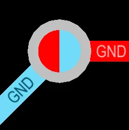
Перемычечные соединения
Перемычечные соединения определяют электрические соединения между площадками компонентов, которые физически не трассируются примитивами на PCB. Они особенно полезны на односторонних платах, где провод используется для перескакивания через дорожки на единственном физическом слое.
Площадкам внутри компонента можно присвоить значение Jumper Jumper в панели Properties. Площадки, имеющие одинаковое значение Jumper и одну и ту же электрическую цепь, сообщают системе, что между ними существует допустимое, хотя и физически не выполненное, соединение.
Перемычечные соединения отображаются в PCB Editor как изогнутые линии соединения. Проверка правил проектирования не будет сообщать о перемычечных соединениях как о нетрассированных цепях.
Особенности переходных отверстий
Определение свойств переходного отверстия
Хотя требования по охвату слоев (Z-plane) для каждого типа переходного отверстия задаются на вкладке the Via Types tab of the Layer Stack Manager, размерные свойства переходного отверстия определяются:
-
ручным редактированием уже размещенного переходного отверстия в панели Properties panel, или
-
PCB default primitives, если переходное отверстие размещается вручную (Place » Via), или
-
правилом проектирования Routing Via Style design rule, если переходное отверстие размещается во время интерактивной трассировки, ActiveRouting или автотрассировки.
Настройка правила проектирования Routing Via Style
Main page: Определение, область действия и управление правилами проектирования PCB
Размерные свойства переходных отверстий, размещаемых во время интерактивной трассировки, ActiveRouting или автотрассировки, контролируются применимым правилом проектирования Routing Via Style. Чтобы упростить выбор переходных отверстий в правиле проектирования, существует набор связанных с переходными отверстиями ключевых слов запросов, которые можно использовать в области действия правила (Where the Object Matches); они подробно описаны ниже.
Когда при трассировке выполняется смена слоя, программное обеспечение анализирует начальный и конечный слои этого перехода и выбирает допустимый тип переходного отверстия из Layer Stack Manager. Затем определяется применимое правило проектирования Routing Via Style с наивысшим приоритетом, и к переходному отверстию, которое должно быть размещено, применяются настройки размера из раздела Constraints этого правила.
Например, у вас может быть набор цепей DRAM_DATA, для которых требуются µVias при переходе между слоями TopLayer - и - S2, а также между слоями S2 - и - S3, и сквозное сверленое переходное отверстие для всех остальных переходов между слоями (которое также отличается от переходного отверстия, необходимого для других цепей). Это можно реализовать, создав два правила проектирования Routing Via Style для этих цепей DRAM_DATA. Ниже показан пример подходящего правила проектирования для µVia; наведите курсор на изображение, чтобы показать правило для сквозного отверстия.

Область действия правил проектирования можно ограничить так, чтобы они применялись к определенным типам переходных отверстий.
Чтобы упростить процесс задания области действия правил проектирования Routing Via Style, доступны следующие ключевые слова запросов, относящиеся к переходным отверстиям:
| Via Type Query | Returns |
|---|---|
| IsVia | Все объекты переходных отверстий, независимо от типа переходного отверстия. |
| IsThruVia | Все переходные отверстия, проходящие от верхнего слоя к нижнему. |
| IsBlindVia | Все переходные отверстия, начинающиеся на внешнем слое и заканчивающиеся на внутреннем слое, которые не являются µVia. |
| IsBuriedVia | Все переходные отверстия, начинающиеся на внутреннем слое и заканчивающиеся на другом внутреннем слое, которые не являются µVia. |
| IsMicroVia | Все переходные отверстия, у которых включена опция µVia и которые соединяют соседние слои. |
| IsSkipVia | Все переходные отверстия, у которых включена опция µVia и которые охватывают 2 слоя. |

Размещение переходных отверстий при интерактивной трассировке
При смене слоев во время интерактивной трассировки программное обеспечение автоматически вставит переходное отверстие. Выбор переходного отверстия зависит от следующего:
- Доступные типы переходных отверстий для слоев, охватываемых при смене слоя.
- Применимое правило проектирования Routing Via Style для типа переходного отверстия, выбранного для данной смены слоя.
Стековые µVias, размещаемые при смене слоя с L1 на L4. Режим Interactive Routing панели Properties отображает тип(ы) переходных отверстий, которые будут размещены; нажмите 6, чтобы циклически переключаться между возможными стеками переходных отверстий; нажмите 8, чтобы вывести список возможных стеков переходных отверстий.
Управление переходным отверстием, размещаемым во время интерактивной трассировки
-
При смене слоев трассировки программное обеспечение автоматически выбирает наиболее подходящий тип переходного отверстия для данного диапазона слоев.
-
Если существует несколько типов/комбинаций переходных отверстий (стеков переходных отверстий), которые можно использовать, нажмите клавишу быстрого вызова 6, чтобы интерактивно циклически переключаться между всеми стеками переходных отверстий, доступными для этой смены слоя; нажмите 8, чтобы вывести список. Стеки переходных отверстий представлены в следующем порядке: использовать µVia, использовать Skip µVia, использовать Blind via, использовать Thruhole via. Стековые переходные отверстия могут размещаться, если смена слоя охватывает более одного слоя и определены подходящие типы переходных отверстий. Предлагаемые типы переходных отверстий подробно отображаются в строке состояния и в Heads Up display, например [µVia 1:2, µVia 2:3, µVia 3:4], как показано на изображении выше.
-
Последний использованный стек переходных отверстий сохраняется как вариант по умолчанию для следующей трассируемой цепи. Стек переходных отверстий по умолчанию сохраняется только на время текущего сеанса редактирования.
-
Размерные свойства переходных отверстий задаются применимым правилом проектирования Routing Via Style design rule; стратегии определения подходящего правила проектирования Routing Via Style рассматривались выше.
-
Чтобы интерактивно изменить размер переходного отверстия при выполнении смены слоя, нажмите сочетание клавиш 4. Это приведет к циклическому переключению режимов размера переходного отверстия:
Rule Minimum;Rule Preferred;Rule Maximum;User Choice; при этом текущий режим Via-Size будет отображаться в Heads Up display и в строке состояния (как показано на изображении выше). Если выбран режим User Choice, нажмите Shift+V, чтобы открыть диалог Choose Via Sizes dialog, и выберите предпочтительный размер переходного отверстия. Список доступных размеров переходных отверстий, отображаемый в диалоге, берется из списка переходных отверстий, уже использованных в проекте; просмотреть их можно в режиме Pad and Via Templates mode панели PCB.Если в применимом правиле проектирования Routing Via Style design rule используется режим Template preferred, сочетание клавиш 4 будет циклически переключать включенные шаблоны переходных отверстий.
-
Вид сбоку предлагаемых типов переходных отверстий отображается в панели Properties, как показано выше.
-
Чтобы разместить переходное отверстие и продолжить трассировку на том же слое, нажмите сочетание клавиш 2.
-
Чтобы разместить переходное отверстие и приостановить трассировку этого соединения, нажмите сочетание клавиш / на цифровой клавиатуре.
-
Если трассируемая цепь должна подключаться к внутренней силовой плоскости, нажмите клавишу / (на цифровой клавиатуре), чтобы разместить переходное отверстие, подключаемое к соответствующей силовой плоскости. Это работает во всех режимах размещения дорожек, кроме режима Any Angle mode.
-
Во время трассировки нажмите Shift+F1, чтобы открыть меню всех горячих клавиш, доступных в текущей команде.
Работа со стековыми переходными отверстиями
-
Составными переходными отверстиями, образующими непрерывное соединение, можно работать как с одним переходным отверстием: click and drag по стеку, чтобы переместить их все вместе с присоединенной трассировкой.
-
Щелкните один раз, чтобы выбрать самое верхнее переходное отверстие в стеке. Если не перемещать мышь, последующие одиночные щелчки будут поочередно выбирать остальные переходные отверстия в этом стеке.
-
Ctrl+Click and drag чтобы переместить только выбранное переходное отверстие вместе с присоединенной трассировкой.
-
Чтобы выбрать все переходные отверстия в стеке, щелкните один раз, чтобы выбрать одно из них, затем нажмите Tab, чтобы расширить выделение и включить в него все переходные отверстия в этом стеке.
Настройка отображения переходных отверстий
Существует ряд параметров отображения, которые помогают работать с переходными отверстиями.
Цвета переходных отверстий
Цвета переходных отверстий настраиваются на панели View Configuration panel. Медное кольцо переходного отверстия отображается в текущем значении Multi-Layer в разделе Layers . Цвет отверстия переходного отверстия отображается в значении Via Holes в разделе System Colors . Также можно отключить отображение отверстий, переключив ![]() для нужного параметра(ов).
для нужного параметра(ов).

Сквозное переходное отверстие показано на первом изображении. Переходное отверстие на втором изображении — глухое; отверстие показано цветами начального и конечного слоев.
Переходные отверстия и паяльная маска
Представление слоев по умолчанию в редакторе PCB таково, что Multi-Layer всегда отображается как самый верхний слой. Это может затруднить точный просмотр содержимого слоев паяльной маски, особенно когда контактная площадка или переходное отверстие использует отрицательное расширение маски, поскольку содержимое слоя паяльной маски скрывается под объектом multi-layer. Это можно изменить, изменив порядок отрисовки слоев на странице PCB Editor – Display диалогового окна Preferences. Установите текущий слой так, чтобы он отрисовывался как самый верхний.
Если изменить порядок отрисовки слоев так, чтобы сверху отображался Current Layer, то при выборе Top Solder в качестве текущего слоя отверстия в маске будут отображаться корректно, как показано на изображении ниже. Зеленые стрелки показывают размер отверстия в паяльной маске для переходного отверстия слева, контактной площадки с уменьшенным отверстием в маске в центре и контактной площадки с увеличенным отверстием справа.

Настройте параметры отображения, чтобы можно было исследовать отверстия в паяльной маске.
Отображение составных переходных отверстий
Если имеются составные переходные отверстия, отображаемые числа соответствуют начальным и конечным слоям всех переходных отверстий в стеке. Наведите курсор на изображение ниже, чтобы показать переходные отверстия в 3D; справа на изображении показан стек из трех переходных отверстий.
 В переходных отверстиях можно отображать охватываемые слои. Наведите курсор, чтобы показать переходные отверстия в 3D.
Другие параметры отображения переходных отверстий
Чтобы отображать имя цепи переходного отверстия и номера слоев в диапазоне переходного отверстия, включите параметры Via Nets и Via Span соответственно в области Additional Options на вкладке View Options панели View Configuration .

Просмотр отверстий контактных площадок и переходных отверстий
В режиме PCB panel’s Hole Size Editor три основные области панели изменяются и отображают следующее (сверху вниз):
- Общую фильтрацию по типам отверстий и их состоянию, с подразделом для пар слоев сверления, определенных в настоящее время для платы.
- Unique Holes сгруппированные по размеру и форме.
- Отдельные Pads/Vias , из которых состоит каждая группа объектов отверстий.

Разделы панели показывают совокупную фильтрацию, примененную к типам, стилям и состоянию отверстий.
Группы отверстий можно редактировать коллективно в области Unique Holes панели, вводя значения в соответствующую ячейку столбца. Можно ввести числовое значение, чтобы изменить текущий размер отверстия для контактных площадок и переходных отверстий в столбце Hole Size .

Изменение размера отверстия для выбранной группы из шести совпадающих стилей отверстий.
Также можно изменить соответствующие значения Hole Length, Hole Type и Plated для отверстий, где это применимо.

Изменение типа отверстия для выбранной группы из шести совпадающих стилей отверстий.
Отдельные объекты контактных площадок/переходных отверстий, относящиеся к выбранной группе отверстий, перечислены в нижнем разделе Pad/Via панели PCB. Щелкните правой кнопкой мыши по объекту в списке и выберите Properties (или просто дважды щелкните по записи), чтобы открыть соответствующий режим панели Properties для этого примитива, где можно просматривать и редактировать его свойства.
Чтобы обновить панель PCB в режиме Hole Size Editor текущими данными символов сверления из PCB, щелкните правой кнопкой мыши в области панели в этом режиме и выберите команду Refresh.
Поддержка обратного сверления
Режим Hole Size Editor панели PCB также можно использовать для просмотра контактных площадок и переходных отверстий, предназначенных для обратного сверления. Пары слоев обратного сверления отображаются в списке Layer Pairs с добавлением текста [BD].
Когда выбран размер отверстия обратного сверления, у объектов параметр Kind отображается как Backdrill. Используйте эту возможность, чтобы быстро находить и проверять отверстия с обратным сверлением. Обратите внимание, что параметры обратного сверления нельзя редактировать на панели.
Отчет по обратному сверлению
Чтобы сформировать отчет по всем событиям обратного сверления, щелкните правой кнопкой мыши в списке Unique Holes и выберите Backdrill Report в контекстном меню.
В отчете приводятся сведения по каждому случаю обратного сверления, включая местоположение, размер сверла и глубину сверления.
Поддержка цековок
Режим Hole Size Editor панели PCB также можно использовать для просмотра контактных площадок с включенными функциями цековки. Если в проекте PCB есть объекты контактных площадок, для которых включены функции цековки (counterbore/countersink) с одной или обеих сторон, соответствующие группы Counterholes Top и/или Counterholes Bottom отображаются в списке Layer Pairs. Столбцы Counterhole Depth и Counterhole Angle можно отобразить в области Unique Holes панели. Обратите внимание, что параметры цековки нельзя редактировать на панели.

Информация о цековках в проекте отображается в режиме Hole Size Editor панели PCB.
 Локализовано с помощью ИИ