PCBは、層のスタックとして設計され形成されます。プリント基板(PCB)製造の初期には、基板は単に絶縁コア層であり、一方または両方の側面に薄い銅層が貼り付けられていました。銅層内で不要な銅を除去(エッチング)することにより、導電性トレースとして接続が形成されます。

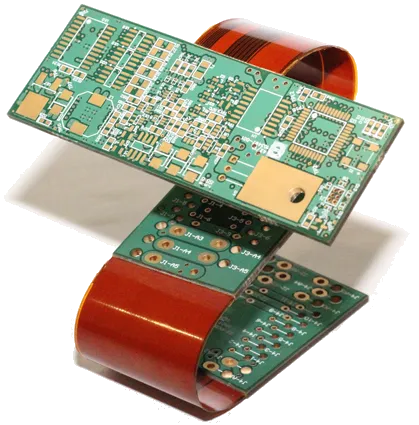
左側に示されているのは、初期のPCB設計に典型的な片面PCBです。右側は、リジッドセクションがフレキシブルなPCBのセクションを介して接続されているリジッドフレックスPCBです。
今日に至るまで、ほとんどすべてのPCB設計は複数の銅層を持っています。技術革新と処理技術の洗練により、フレキシブルPCBを設計および製造する能力を含む、PCB製造における数々の革命的な概念が生まれました。リジッドセクションをフレキシブルセクションを介して結合することにより、複雑なハイブリッドPCBが設計され、通常の形状の筐体に収めるために折りたたむことができます。
プリント基板設計において、レイヤースタックは、垂直方向またはZ平面において層がどのように配置されるかを定義します。単一のエンティティとして製造されるため、リジッドフレックスボードを含む任意のタイプのボードは、単一のエンティティとして設計されなければなりません。これを行うために、設計者は複数のPCBレイヤースタックを定義し、リジッドフレックス設計の異なるゾーンに異なるレイヤースタックを割り当てることができる必要があります。
リジッドフレックス設計についてもっと学ぶ
Layer Stack Manager
PCBレイヤースタックの定義は、成功したプリント基板設計の重要な要素です。現代の多くのPCBの配線は、単純な銅の接続のシリーズではなく、回路要素または伝送線のシリーズとして設計されています。
成功した高速PCB設計を達成することは、適切な片面および差動配線インピーダンスを達成するために必要な配線寸法とクリアランスに対して、材料選択とレイヤースタックアップおよび割り当てをバランスさせるプロセスです。また、レイヤーペアリング、慎重なビア設計、可能なバックドリリング要件、リジッド/フレックス要件、銅バランス、レイヤースタックの対称性、および材料の適合性を含む、現代の高速PCBを設計する際に考慮すべき多くの他の設計上の考慮事項があります。
Layer Stack Managerは、これらすべての層固有の設計要件を単一のエディタに組み合わせます。
Layer Stack Managerを開くには、PCBエディタのメインメニューからDesign » Layer Stack Managerを選択します。

レイヤースタック管理のすべての側面は、Layer Stack Managerで実行されます。
Layer Stack Managerは、次の用途に使用されます:
-
信号層、プレーン層、および誘電体層の追加、削除、および順序付け。
-
材料ライブラリから材料特性を選択するか、手動で設定します。
-
レイヤースタックに追加のユーザー定義フィールドを追加します。
-
許可されるビアタイプを設定し、各ビアタイプが跨ぐ層を定義します。
-
制御インピーダンス配線が使用されている場合、インピーダンスプロファイルを設定します。
-
リジッドフレックス設計、プリントエレクトロニクス、バックドリリングなどの高度な機能を設定します。
Layer Stack Managerは、回路図シート、PCB、および他のドキュメントタイプと同じようにドキュメントビューで開きます。ボードの作業中に開いたままにしておくことができ、ボードとLSMの間を行き来することができます。画面の分割や別のモニターでの開き方など、標準のビュー動作がサポートされています。
Layer Stack ManagerでSaveアクション(File » Save to PCB、ショートカット:Ctrl+S)を実行する必要があります。変更がPCBに反映される前に。
機能は、Layer Stack Managerの下部に表示されるいくつかのタブに分かれています:
Stackupタブ - すべての層のレイヤー特性を追加、削除、および設定
Stackupタブは製造層の詳細を示します。層はこのタブで追加、削除、および設定されます。リジッドフレックス設計の場合、層はこのタブでも有効/無効にされます。
► Propertiesパネルでのスタックアップの設定
最大32のシグナルレイヤーと16のプレーンレイヤーを追加できます。必要に応じて、プレーンレイヤーは任意の回数分割でき、分割内分割エリアを定義できます:詳細を学ぶ。
Impedance Tab - インピーダンスプロファイル要件の設定
このタブは、インピーダンスプロファイルを定義するために使用され、配線設計ルールと共に使用できます。
-
Impedanceタブをクリックして、Layer Stack Managerの下部にあるインピーダンスプロファイルの要件を設定します。インピーダンスプロファイルが設定されたら、必要なプロファイルを配線幅または ![]() 差動ペア配線の設計ルールで選択できます。
差動ペア配線の設計ルールで選択できます。
-
 をクリックするか(またはプロファイルがまだ追加されていない場合はAdd Impedance Profileボタン)、新しい
 ![]() インピーダンスプロファイルを追加し、Type、Target Impedance、Target ToleranceをPropertiesパネルで定義します。Descriptionはオプションです。
インピーダンスプロファイルを追加し、Type、Target Impedance、Target ToleranceをPropertiesパネルで定義します。Descriptionはオプションです。
-
次のステップは、現在選択されているプロファイルが利用可能になるレイヤーを定義することです。グリッドは2つのゾーンに分かれています:スタックアップ内のレイヤーが左に表示され、現在選択されているインピーダンスプロファイルが利用可能になるレイヤーが右に表示されます。選択したインピーダンスプロファイルのためにそのレイヤーを利用可能にするには、インピーダンスプロファイル領域のレイヤーチェックボックスを使用します。
-
インピーダンスプロファイル領域で有効なレイヤーを選択すると、その選択された信号レイヤーのインピーダンスを計算するために使用されるレイヤーを除いて、レイヤースタック内のすべてのレイヤーが薄暗く表示されます(画像を表示![]() )。
)。
-
レイヤーにインピーダンスプロファイルが割り当てられたら、Top RefおよびBottom Ref列でそのレイヤーのリファレンスレイヤーを編集します。リファレンスレイヤーはTypeプレーンまたはシグナルであることに注意してください。
-
インピーダンス計算機は、前方および逆方向のインピーダンス計算をサポートしています。Target Impedanceを入力すると、Widthが自動的に変更されます(前方計算)、またはWidthを入力すると、Target Impedanceが自動的に変更されます(逆計算)。
-
差動インピーダンス計算の場合、適切な  ボタンをクリックしてWidthまたはTrace Gapのいずれかをロックします。ロックされていない変数は、Target Impedance値が変更されると計算されます。または、ロックされていない変数を編集してTarget Impedanceを変更します。
-
Etch Factor = Thickness/[(W1-W2)/2](パネル内の?にカーソルを合わせると式が表示されます)
-
インピーダンス計算機は、複数の隣接する誘電体層をサポートしています。これらの層は異なる誘電特性を持つことができます。
-
ストリップライン構造の場合、誘電体の高さは銅層間の距離として計算されます(画像のH2を参照![]() )。
)。
-
差動インピーダンス計算機は、非対称ストリップライン構造をサポートしています。
-
Simbeorインピーダンス計算機は、単一および差動コプレーナ構造をサポートしています。
-
すべての計算は1GHzの周波数を使用して行われます。
-
計算速度を向上させるために、インピーダンスプロファイルは(可能な場合)別のスレッドで計算されます。
Via Typesタブ - ビアのZ平面レイヤー跨ぎ要件を定義する
Via Typesタブは、設計で使用されるビアのZ平面レイヤー跨ぎ要件を定義するために使用されます。デザインに配置されたビアの直径と穴サイズ(X&Yプロパティ)は、ビアが手動で配置された場合はデフォルトの設定によって、またはビアがインタラクティブ配線中に配置された場合は適用される配線スタイル設計ルールによって制御され続けます。
-
新しいボードのレイヤースタックには、Layer Stack ManagerのVia Typesタブに単一のスルーホールビアスパン定義が含まれています。2層ボードの場合、デフォルトのビアはThru 1:2と名付けられ、ビアタイプとビアが跨ぐ最初と最後のレイヤーを反映しています。デフォルトのスルーホールスパンは削除できません。
-
ボタンをクリックして追加のビアタイプを追加し、プロパティパネルでこのビアタイプが跨ぐレイヤーを選択します。新しい定義µViaが必要な場合は、µViaチェックボックスを有効にします。このオプションは、ビアが隣接するレイヤーまたは隣接する+1(スキップビアと呼ばれる)にまたがる場合にのみ利用可能です。
-
レイヤースタックにStack Symmetryオプションが有効になっている場合、Mirrorオプションが利用可能になります。Mirrorが有効になると、レイヤースタック内の対称レイヤーにまたがる現在のビアのミラーが自動的に作成されます。
-
ワークスペースに配置されたビアには、Nameプロパティのドロップダウンが含まれており、Layer Stack Managerで定義されているすべてのビアタイプがリストされます。ボードで使用されるすべてのビアは、Layer Stack Managerで定義されたビアタイプのいずれかでなければなりません。
-
インタラクティブ配線中にレイヤーを変更するとき:
-
プロパティパネルが適用可能なビアタイプを表示します(画像を表示
![]() )。
)。
-
複数のビアタイプが適用されるレイヤーに対応している場合は、6のショートカットを押して、利用可能なビアタイプを切り替えます。
-
提案されたビアタイプはステータスバーに詳細が表示されます(画像を表示
![]() )。
)。
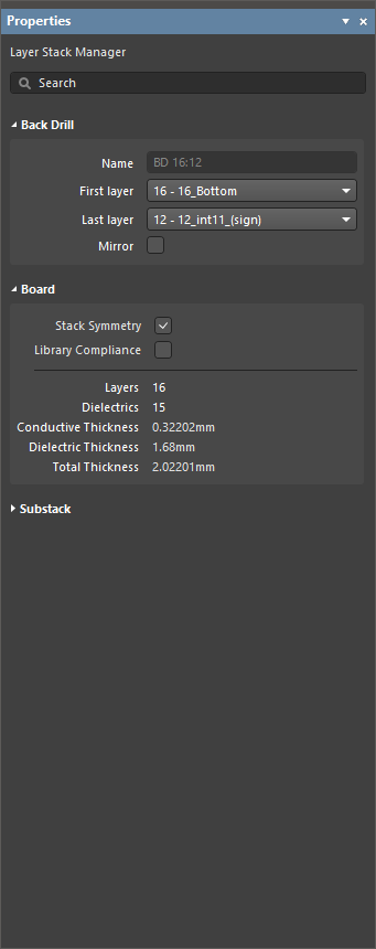
Back Drillsタブ - バックドリルが必要とされるレイヤースパンを定義
高速設計では、ビアのバレルが信号が配線されている信号レイヤーを超えて延びると、信号反射が発生することがあります。これは信号劣化や信号整合性の問題につながる可能性があります。これを解決する一つの方法は、制御深度ドリリングとも呼ばれる技術を使用して、使用されていないビアバレルをドリルアウトすることです。
-
バックドリルのプロパティは、Back Drillsタブで設定され、このタブはTools » Featuresサブメニューでバックドリルが有効になっている場合、または  ボタンをクリックしてBack Drillsを選択すると表示されます。
-
Back Drillsタブは、パッドまたはビアスタブが存在する場合にバックドリルが必要とされるレイヤースパンを定義するために使用されます。これらの設定は、最大スタブ長とドリルオーバーサイズ量が指定される最大ビアスタブ長設計ルールと共に使用されます。Where the Object Matchesルールの設定を使用して、特定のネットに対してスタブ除去を制限することができます。
-
ボタンをクリックして新しいバックドリル定義を追加します。定義は、プロパティパネルのBack Drillセクションで選択されたFirst layerとLast layerに応じて命名されます。例えば、BD 1:3。First layerはドリルされる最初のレイヤーを定義し、Last layerはドリルが停止する前のレイヤーを定義します(Last layerはレイヤースタック内でバックドリルされない最初のレイヤーです)。
-
サブスタックプロパティがPropertiesパネルでStack Symmetryオプションを有効にしている場合、Back DrillセクションのパネルでMirrorオプションが利用可能になります。これが有効になると、現在のバックドリルのミラーが作成されます。例えば、BD 1:3 | 6:4。
Printed Electronics Stackupタブ - 印刷された設計のためのレイヤーを構成
現代の印刷技術を使用すると、基板材料に直接導電性および非導電性のレイヤーを印刷し、電子回路を構築することが可能です。これはプリンテッドエレクトロニクスとして知られています。
-
レイヤースタックは、Tools » Features » Printed Electronicsオプションを選択することでプリンテッドエレクトロニクス用に構成されます。このモードでは、すべてのタブが単一のPrinted Electronics Stackupタブに置き換えられます。
-
従来の誘電体層は、プリンテッドエレクトロニクスでは使用されません。代わりに、ルーティングがクロスオーバーする必要がある場所で、ローカル誘電体パッチが印刷されます。FeaturesドロップダウンでPrinted Electronicsオプションを有効にすると、すべての誘電体層がレイヤー・スタックから削除され、代わりに、非導電層上に適切な形状の領域オブジェクトを配置することで誘電体パッチが定義されます。
-
プリンテッドエレクトロニクスでは、銅信号層は導電層として、絶縁層は非導電層として参照されます。
ボードタブ - リジットフレックス設計でのサブスタックの作成と設定
ボードタブは、リジットフレックス設計に必要な異なるサブスタックを設定するために使用されます。ボードタブは、リジットフレックス(高度)モードが有効になると自動的に表示されます。標準のリジットフレックスモードが選択された場合には使用/利用できません。
Layer Stack Managerのボードタブは、以下のために使用されます:
-
サブスタックの追加。追加のサブスタックは、必要な層を選択するためにShift+Clickショートカットを使用し、選択を水平にドラッグしてサブスタックのセットに配置することで、既存のサブスタックから迅速に作成できます。
-
隣接するサブスタック内の層間の関係を設定します。例えば、層が共有されているか(共通)、そのサブスタック内の層がユニークか(個別)。
-
隣接する層が隣のサブスタックに侵入するかどうかを設定します。
-
特定のサブスタックの編集に切り替える - ボードタブでそれをダブルクリックすることでこれを行います。
-
追加のブランチを追加します。ブランチは、設計が単一の剛体セクションから放射する複数の柔軟なセクションを持つ場合に使用されます。ブランチについてもっと学ぶ。
ボードタブは、高度なリジットフレックスモードの一部として導入されました。高度なリジットフレックスモードは、重なり合う柔軟な板と剛体板の領域、新しいボード領域と曲げ線の挙動、およびLayer Stack Managerのボードタブの導入などの設計機能をサポートします。以下に示すように、Layer Stack Managerで関連するコマンドを選択することにより、標準のリジットフレックスモードと高度なリジットフレックスモードの間で切り替えることができます。
。") 標準または高度なリジットフレックスモードを選択すると、インターフェースが変更されます(画像にカーソルを合わせると違いが表示されます)。
標準または高度なリジットフレックスモードを選択すると、インターフェースが変更されます(画像にカーソルを合わせると違いが表示されます)。
►リジットフレックスPCBの設計についてもっと学ぶ。
アクティブなレイヤースタックで測定単位を変更するには、Tools » Measurement Unitsを選択し、希望する測定単位(mil、in、µ、またはmm)を選択するか、Ctrl+Qキーボードショートカットを使用して測定単位を切り替えます。
レイヤースタックプロパティの編集
Layer Stack Managerは、スプレッドシートのようなグリッドで層のプロパティを提示します。プロパティはグリッド内で直接編集することも、Propertiesパネルで編集することもできます。このパネルは、Layer Stack Managerの各タブで使用でき、例えばImpedanceタブやVia Typesタブのインピーダンスプロファイルや伝送線プロパティ、µVia設定にアクセスできます。


プロパティパネルのいくつかのモードLayer Stack Manager
プロパティパネルは、ソフトウェアの右下にある ボタンを介して有効/無効にすることができます。
レイヤースタックドキュメントのStackupタブがアクティブな場合、Propertiesパネルを使用してレイヤースタックの層プロパティを編集できます。

-
Name – 層の名前。
-
Manufacturer – 層の製造者。
-
Material – 層の材料。これは、Altium Material Libraryダイアログ(Tools » Material Libraryフィールドで事前に定義されるか、レイヤースタックでユーザー定義されます。 をクリックして、レイヤースタック内で現在選択されている層に対して希望の材料を選択するためのSelect Materialダイアログを開きます。
-
Thickness – 信号層の厚さ。
-
Dk - これは誘電率定数(電磁気学ではεrとも呼ばれます)。これは絶縁材料の相対誘電率を示し、電場内での電気エネルギーの蓄積能力を指します。絶縁目的では、誘電率定数が低い材料が望ましく、RFアプリケーションでは、高い誘電率定数が望ましい場合があります。さらに、相対誘電率定数が低いほど、その材料の性能は空気に近くなります。この特性は、特定の伝送線のインピーダンス要件に合わせるために重要です。
-
Df - これは損失係数です。これは、機械的、電気的、または電気機械的振動など、特定の振動モードにおけるエネルギー損失の割合を示すことにより、絶縁材料の効率を示します。言い換えると、これは材料が伝達されたエネルギーのどれだけを吸収するかを記述する材料の特性です。損失正接が大きいほど、材料へのエネルギー吸収が大きくなります。この特性は、高速での信号減衰に直接影響します。
-
Process - PCBの外側の信号層(トップレイヤーとボトムレイヤー)を構成する基板銅に適用される銅めっきプロセスを表示します。
-
Weight - 単位面積あたりの銅の重量で、通常はオンス/平方フィート(例:0.5 oz/ft2)で表されます。
-
Orientation - このレイヤー上でコンポーネントがどのように向いているか(向き)を定義します。トップサイドとボトムサイドについては、新しいボードでは自動的に設定されます。他の信号層では、以下の用途に使用されます:
-
リジッドフレックス設計では、フレックスセクションの表面層となる内部信号層にコンポーネントが取り付けられる場合、ソフトウェアはこれらのコンポーネントがどの方向を向いているかを知る必要があります。必要な向きを選択するためにドロップダウンを使用します。選択肢には、Not allowed、Top、およびBottomが含まれます。
-
埋め込みコンポーネントを含む設計では、ソフトウェアはコンポーネントがどの方向を向いているかを知る必要があります。埋め込みコンポーネントを使用したPCBの設計ページを参照して、レイヤースタックでのコンポーネントの向きを設定する情報について確認してください。必要な向きを選択するためにドロップダウンを使用します。選択肢には、Not allowed、Top、およびBottomが含まれます。
-
Copper Orientation - これは銅がコアにラミネートされる方向を定義します。上または下を選択するためにドロップダウンを使用します。これはエッチングされる方向を決定します。
Copper Orientationは、
Layer Stackの
Copper Orientation列のドロップダウンを使用して選択することもできます。列を有効にするには、ヘッダーで右クリックし、
Select columnsを選択してから、
Select columns dialogで
Copper Orientationエントリを有効にします。また、
Impedance Profileモードのパネルで
Trace Invertedオプションを使用して銅の向きを設定することもできます。
向きは、PropertiesパネルのStackupモードでCopper Orientationドロップダウンを使用するか、現在表示されている場合はCopper Orientation列、またはPropertiesパネルのImpedance ProfileモードでTrace Invertedチェックボックスを使用して設定できます。
-
Pullback Distance - 平面エッジからボードエッジまでの距離です。
-
Frequency - 材料がテストされ、Dk / Dfが特定の周波数に対応する周波数です。周波数は材料の参照からも取得されます。
-
Description - 意味のある説明を入力します。
-
Constructions - 誘電層について、層の構造を表示します。数値参照は、誘電層材料に使用される織りガラスファブリックの構造に関連しており、これらはPCB製造業者によって使用される標準的な参照です。
-
Resin - 層の樹脂の割合を表示します。
構造と樹脂に関する注意事項:
積層構造の選択は、コストと性能の両方に大きな影響を与える可能性があります。予想される通り、単層構造は通常、複数層構造と比較してコスト削減を意味します。これらの節約の大きさは、関与する特定のガラススタイルやその他多くのパラメーターに依存します。性能も影響を受ける可能性があり、使用する構造を指定する際には考慮されるべきです。まず、単層構造はしばしば樹脂含有量が低くなります。単層構造のもう一つの主な利点は、樹脂含有量を超えた誘電体厚さの制御です。単層構造を使用することで、より厳密な厚さの公差が達成できます。
比較的樹脂含有量が低い構造は、Z軸方向の膨張が少なくなり、多くのアプリケーションで信頼性が向上するため、しばしば好まれます。さらに、樹脂含有量が低いと、寸法安定性、反りへの抵抗性、誘電体厚さの制御も改善されます。一方、樹脂含有量が高い構造は、誘電定数値が低くなり、電気性能のために時々好まれます。さらに、適切な樹脂含有量が必要で、ラミネート内に空隙が発生するのを防ぎ、ガラス繊維を樹脂で完全に湿潤させるためです。ガラス繊維を樹脂で完全に湿潤させる能力は、CAP耐性にも重要です。
-
Material Frequency – これは材料がテストされる周波数であり、Dk / Dfが特定の周波数に対応する値です。周波数は材料の参照からも取得されます。
-
GlassTransTemp – これはガラス転移温度(TGとしても知られています)であり、樹脂がガラス状態から非晶質状態に変化し、その機械的挙動、すなわち膨張率を変える温度です。
-
Note – レイヤーに関する重要な注記を入力します。
-
Comment – レイヤーに必要なコメントを入力します。
-
Stack Symmetry – レイヤースタックの対称性を維持するために有効にします。レイヤースタックの対称性セクションを参照して詳細を学びましょう。
-
Library Compliance – 有効にすると、材料ライブラリから選択された各レイヤーについて、現在のレイヤーのプロパティがライブラリ内のその材料定義の値と照合されます。
-
Substack – これは現在選択されているサブスタック(レイヤー、誘電体、厚さなど)に関する情報です。サブスタックを切り替えると、この情報はそれに応じて更新されます(現在選択されているサブスタックについて)。
Rigid/FlexオプションがFeaturesドロップダウンで有効にされている場合にのみ、Substack領域が利用可能になります。
-
Stack Name – サブスタックの名前を入力します。X/Yスタックアップ領域にレイヤーサブスタックが割り当てられる場合、サブスタックに名前を付けると便利です。
-
Is Flex – サブスタックがフレックスである場合に有効にします。
-
Layers – 導電性レイヤーの数。
-
Dielectrics – 誘電体の数。
-
Conductive Thickness – すべての信号層とプレーン層(すべての銅または導電性レイヤー)の厚さの合計です。
-
Dielectric Thickness – 誘電体層の厚さ。
-
Total Thickness – 完成したボードの総厚さ。
-
Roughness – 導電性レイヤーの粗さを示します。
-
Model Type – 表面粗さの影響を計算するための好ましいモデル(詳細については、以下の記事を参照してください)。スタック内のすべての銅層に適用されます(サブスタックであるべきですか?)。
-
Surface Roughness – 表面粗さの値(製造業者から入手可能)。0から10µmの間の値を入力してください、デフォルトは0.1µmです
-
Roughness Factor – 粗さ効果による導体損失の予想される最大増加を特徴づける値。1から100の間の値を入力してください;デフォルトは2です。
-
Copper Resistance - 銅の抵抗値(nOhms)。
-
Via Plating Thickness - ビアめっきの総厚さ。
他のレイヤースタックタブで利用可能なオプションとコントロールについて詳しく知るには、以下のリンクを使用してください:
レイヤースタックの定義
StackupタブのLayer Stack Managerで追加したレイヤーは、製造プロセス中に製造されるレイヤーです。
 レイヤーのプロパティは、グリッドに直接入力するか、または材料ライブラリから選択できます。
レイヤーのプロパティは、グリッド内またはプロパティパネルで直接編集できます。
レイヤープロパティと材料の設定
各レイヤーのプロパティは、LSMグリッド内で直接編集するか、または材料ライブラリから事前定義された材料を選択できます。選択したレイヤーのMaterialセル内の省略記号ボタン( )をクリックします。このページの前半にあるスタックアップタブの折りたたみセクションは、レイヤーの追加、削除、編集、並べ替えに利用可能なさまざまな技術を要約しています。
ユーザー定義のプロパティ列を追加し、すべての列の表示をSelect columnsダイアログで設定できます。ダイアログを開くには、グリッド領域の任意の列見出しを右クリックし、コンテキストメニューからSelect columnsを選択します。

Select columnsダイアログ
Select columnsダイアログのオプションとコントロール
-
フィルター - リストをフィルタリングするために文字を入力します。
-
リスト - Layer Stack Managerに表示可能なすべての列のリストです。項目が を表示する場合、その列はLayer Stack Managerに表示されます。項目が
 を表示する場合、その列はLayer Stack Managerに表示されません。表示/非表示機能を切り替えるには、記号をクリックします。
-
Up/Down - 選択した項目をリスト内で上または下に移動します。これにより、Layer Stack Manager内で列が表示される順序が決まります。
-
Add - 新しい列を追加するにはクリックします。新しい列としてCustom[n]がColumnリストに追加されます。新しい列エントリを選択してからEditをクリックし、必要に応じて名前を変更します。
-
Edit - 選択した列を編集するにはクリックします。これは追加されたカスタム列にのみ利用可能です。システム列は編集できません。
-
 - 選択した列を削除するにはクリックします。これは追加されたカスタム列にのみ利用可能です。システム列は削除できません。
レイヤータイプとそのプロパティ
プリント回路基板の製造には、多種多様な材料が使用されます。以下の折りたたみセクションの表は、一般的に使用される材料の簡単な要約を示しています。
レイヤータイプとそのプロパティの要約
レイヤー材料とそのプロパティの選択は、常に基板製造業者と相談して行うべきです。
| レイヤータイプ |
使用される材料 |
コメント |
| シグナル |
銅 |
電気信号と回路供給電流を運ぶために使用される銅層。通常はアニール処理された箔や電気めっきされたもの。 |
| 内部プレーン |
銅 |
電力とグラウンドを分配するために使用される固体銅層。領域に分割することもできます。また、プレーンエッジから基板エッジまでの距離(プルバック)も指定する必要があります。通常はアニール処理された箔。 |
| 表面仕上げ |
様々、電気ニッケル浸金(ENIG)、ホットエアーはんだレベリング(HASL)、無鉛(HASL)、浸錫、有機はんだ付け性保存剤(OSP)/Entek、ハードゴールド、 浸銀
|
露出した外側の銅層に適用されます。銅の酸化を防ぎ、はんだ付けのための良好な表面を提供する二つの機能があります。各仕上げタイプにはそれぞれ長所と短所がありますが、最も人気のあるのは高品質ではんだ付け性が良く、コストが低いENIGです。 |
| 誘電体 |
FR4、ポリイミド、および異なる設計パラメータを提供するメーカー固有の材料を含む様々なもの |
絶縁層;剛性または柔軟性があります。コア、プレプレグ、および柔軟な層を定義するために使用されます。
重要な機械的特性には、湿度および温度範囲における寸法安定性、引裂き抵抗、および柔軟性が含まれます。
重要な電気的特性には、絶縁抵抗、誘電率(Dk)、および損失係数(損失正接、DfまたはDj)が含まれます
|
| オーバーレイ |
スクリーン印刷エポキシ、LPI(液体フォトイメージャブル) |
コンポーネント指定子、ロゴ、製品名などのテキスト/アートワークを表示します。 |
はんだマスク/カバーレイ
|
1) はんだマスク - 液体フォトイメージャブルはんだマスク(LPIまたはLPSM)、ドライフィルムフォトイメージャブルはんだマスク(DFSM)
2) カバーレイ - 通常はポリイミドまたはポリエステルの接着剤コーティングされた柔軟なフィルム。
|
1) はんだが適用される場所を制限する保護層。剛性およびフレックス使用クラスA(フレックス・トゥ・インストール)アプリケーションに適した、コスト効果的で実証済みの技術。柔軟なフィルムカバーレイよりも細かい特徴に適しています。
2) フレックス使用クラスAおよびB(ダイナミックフレックス)に適しています。通常、穴や角は丸くされ、ドリルまたはパンチで作られます。
|
| ペーストマスク |
ペーストマスクステンシルが製造される層。ステンシルは通常ステンレス鋼です。ステンシルの開口部は、コンポーネント配置前にコンポーネントパッドにはんだペーストを適用する場所を定義します。 |
マスク層は、はんだペーストを適用する場所を定義するはんだマスクスクリーンの製造に使用されます。 |
材料ライブラリとライブラリコンプライアンス
好ましい層スタック材料は、材料ライブラリで事前に定義することができます。Layer Stack Managerで、Tools » Material Libraryを選択してAltium Material Libraryダイアログを開き、既存の材料を確認したり新しい材料定義を追加することができます。

Altium Material Libraryダイアログ
Altium Material Libraryダイアログのオプションとコントロール
-
 /
/  - 前の操作を元に戻すまたはやり直すためにクリックします。下矢印を使用して、選択できる以前の操作のリストにアクセスします。
-
単位 - 希望の単位を選択します。サポートされている単位は mil、in、 µm、およびmmです。
-
 - Material Library Settingsダイアログを開いて、ダイアログに表示される列を選択します。
-
左側の領域 - このツリーには利用可能な材料タイプが表示されます。アイテムをクリックすると、右側のグリッドに詳細が表示されます。
-
グリッド - 左側の領域で選択されたアイテムの利用可能な材料が表示されます。ヘッダーの をクリックして、結果として表示されるドロップダウンで希望のフィルタを選択して列をフィルタリングします。
-
Load- 外部材料ライブラリデータベース(*.xml)からユーザー定義の材料を検索して選択し、ダイアログに読み込むためのダイアログを開きます。
-
Save- ユーザー指定の材料を材料ライブラリデータベース(*.xml)に保存します。
-
New- ユーザー定義の材料を追加します。新しい材料定義は、左側のツリーで材料タイプが選択されている場合に利用可能で、そのSourceプロパティはUserに設定されます。
-
Edit- 選択されたユーザー定義の材料を編集します。
-
- 選択されたユーザー定義の材料を削除します。
特定の層の材料は、Altium Material Libraryダイアログで選択されません。層に特定の材料を使用するには、層スタックグリッドのMaterialsセルの層の省略記号()をクリックするか、層が層スタックグリッドで選択されているときにMaterial フィールドの をクリックします。これにより、Select Materialダイアログが開き、省略記号コントロールがクリックされた層に適した材料のみをライブラリに表示するように制限されます。

Select Materialダイアログ
Altium Material LibraryダイアログまたはSelect Materialダイアログに表示される列を選択するには、 ボタンをクリックしてMaterial Library Settingsダイアログを開きます。

Material Library Settingsダイアログ
Material Library Settingsダイアログのオプションとコントロール
-
フィルタ - Columnリストをフィルタリングするために文字を入力します。
-
Column - Altium Material LibraryダイアログまたはSelect Materialダイアログに表示可能なすべての列のリストです。項目が  表示されると、その列はAltium Material Libraryダイアログまたは材料選択ダイアログに表示されます。項目が
 表示されない場合、その列はダイアログに表示されません。表示/非表示機能を切り替えるには、記号をクリックします。
-
Add - 新しい列を追加するにはクリックします。新しい列としてCustom[n]がColumnリストに追加されます。新しい列エントリを選択してから、名前を変更する場合はEditをクリックします。
-
Edit - 選択した列を編集するにはクリックします。これは追加されたカスタム列にのみ利用可能です。システム列は編集できません。
-
- 選択した列を削除するにはクリックします。これは追加されたカスタム列にのみ利用可能です。システム列は削除できません。
-
Up/Down - 選択した項目をColumnリストの中で上または下に移動するにはクリックします。これにより、列がAltium Material LibraryダイアログまたはSelect Materialダイアログに表示される順序が決まります。
Library ComplianceチェックボックスがLayer Stack Managerで有効になっている場合、材料ライブラリから選択された各レイヤーについて、現在のレイヤー属性がライブラリ内のその材料定義の値と照合されます。準拠していないプロパティはエラーフラグでマークされます。材料を再選択()して、値を材料ライブラリの設定に更新します。
レイヤースタックの対称性
ボードのレイヤースタックを対称にする必要がある場合は、Stack SymmetryチェックボックスをBoard領域のプロパティパネルで有効にします。これが行われると、レイヤースタックは中央の誘電体層を中心に直ちに対称性がチェックされます。中央の誘電体基準層から等距離にある任意のレイヤーペアが同一でない場合、Stack is not symmetricダイアログが開きます。

ダイアログの上部にあるLayer stack symmetry mismatchesグリッドは、レイヤースタックの対称性に関するすべての検出された衝突を詳細に説明します。
ダイアログの下部には、レイヤースタックの対称性を達成するための以下のオプションが提供されます:
-
Mirror top half down - 中央の誘電体層の上にある各レイヤーの設定が、対称パートナーレイヤーにコピーされます。
-
Mirror bottom half up - 中央の誘電体層の下にある各レイヤーの設定が、対称パートナーレイヤーにコピーされます。
-
Mirror whole stack down - 最後の銅(Surface Finish)層の後に追加の誘電体層が挿入され、その後、すべての信号層と誘電体層がこの新しい誘電体層の下に複製されてミラーされます。
-
Mirror whole stack up - 最初の銅(Surface Finish)層の前に追加の誘電体層が挿入され、その後、すべての信号層と誘電体層がこの新しい誘電体層の上に複製されてミラーされます。
スタック対称が有効になっている場合:
-
レイヤー属性に適用された編集アクションは、対称のパートナーレイヤーに自動的に適用されます。
-
レイヤーを追加すると、対応する対称のパートナーレイヤーが自動的に追加されます。
Stack Symmetryオプションを使用して、レイヤースタックの半分を定義し、Stack Symmetryオプションを有効にしてから、全スタックをミラーするオプションのいずれかを使用して、そのレイヤーセットを複製することで、対称のボードを簡単に定義できます。
レイヤースタックの可視化
レイヤースタックを3Dで可視化することは、レイヤースタックを確認する絶好の方法です。Layerstack Visualizerダイアログを使用すると、レイヤースタックを2Dまたは3Dで見ることができます。

-
Tools » Layerstack Visualizerを選択して、Layer Stack ManagerでLayerstack Visualizerを開きます。
-
レイヤースタックの表示を設定するためのコントロールを使用します。
-
右クリックしてドラッグすると、ビジュアライザー内のボードの向きを変更できます。
-
画像を左クリックしてからCtrl+Cで、画像をWindowsクリップボードにコピーします。
Layerstack Visualizerダイアログのオプションとコントロール
-
2D/3D - レイヤースタックをどのビューで見たいか選択します。
-
Orthographic camera - 直交投影を使用して表示するには有効にします。透視投影を使用して表示するには無効にします。
-
Show full stack - フルスタックを表示するにはチェックします。
-
Show layer names - レイヤー名を表示/非表示にするにはチェック/チェック解除します。
-
Real layers height - レイヤーの実際の高さを表示するにはチェック/チェック解除します。
-
Space between layers - レイヤー間にスペースを表示するにはチェック/チェック解除します。
-
Simple conductors - シンプルな導体で表示するにはチェックします。
リジッドフレックスサブスタックの定義と設定
メインページ: リジッドフレックス設計
リジッドフレックスは現在積極的に開発されており、現在2つのリジッドフレックス設計モードをサポートしています。従来の、または標準モードと呼ばれるリジッドフレックスは、シンプルなリジッドフレックス設計をサポートします。設計が重なり合うフレックス領域など、より複雑なリジッドフレックス要件を持つ場合は、Advancedリジッドフレックスモード(リジッドフレックス2.0とも呼ばれます)が必要です。Advancedモードには、重なり合うフレックス領域だけでなく、サブスタックの視覚的定義、リジッドおよびフレキシブルボード領域の定義の容易化、ネストされたカットアウト上の曲げ、カスタム形状の分割、ブックバインダー型構造のサポートも含まれます。必要なモードは、以下に示すようにLayer Stack Managerで選択されます。
標準またはAdvancedリジッドフレックスモードを選択すると、インターフェースが変更されます(画像にカーソルを合わせると違いが表示されます)。
►リジッドフレックスPCBの設計についてもっと学ぶ。
リジッドフレックス設計の各別のゾーンまたは領域は、異なる数のレイヤーで構成されることがあります。それを実現するには、サブスタックと呼ばれる複数のスタックを定義できる必要があります。

標準リジッドフレックス設計でのサブスタックの追加
-
Tools » Features » Rigid/Flexコマンドを選択してリジッドフレックスオプションを有効にします。このコマンドは、機能(  )メニューからもアクセスできます。
-
標準リジッドフレックスモードで作業している場合、表示はStackupタブに留まりますが、画像に示すように、サブスタックの選択と管理ボタンが上部に表示されます。
-
全体のボードのリジッドフレックスサブスタックの場合、Is Flexオプションをプロパティパネルで有効にします。フレックス専用のカバーレイ層は、Is Flexオプションが有効になっており、かつソルダーマスク層が含まれていないサブスタックにのみ追加できます。

高度なリジッドフレックス設計でのサブスタックの追加
-
Tools » Features » Rigid/Flex (Advanced)コマンドを選択して、リジッドフレックスオプションを有効にします。このコマンドは、機能( )メニューからもアクセスできます。
-
高度なリジッドフレックスモードでは、表示がBoardタブに切り替わります。
-
全体のボードのリジッド領域とフレックス領域で必要な各ユニークな層のセットに対して、ユニークなサブスタックを定義する必要があります。ボードモードは、高度なリジッドフレックス設計に必要な異なるサブスタックを設定するために使用されます。
-
既存のサブスタックから追加のサブスタックを素早く作成するには、Shift+Clickショートカットを使用して必要な層を選択し、次に選択を水平にドラッグしてサブスタックのセットに配置します。
-
隣接するサブスタックの層間の関係を設定します - 例えば、層が共有されていますか(共通)、それともそのサブスタック内の層はユニークですか(個別)?
-
隣接する層が隣のサブスタックに侵入するかどうかを設定します。
-
特定のサブスタックの編集に切り替えます - これを行うには、ボードタブでダブルクリックします。
-
追加のブランチを追加します。ブランチは、設計に複数のフレックスセクションが単一のリジッドセクションから放射する場合に使用されます。
-
フレックスサブスタックの場合、Is Flexオプションをプロパティパネルで有効にします。フレックス専用のカバーレイ層は、Is Flexオプションが有効になっており、かつソルダーマスク層が含まれていないサブスタックにのみ追加できます。

►リジッドフレックスPCBの設計についてもっと学ぶ
シングルレイヤーPCBサポート
2層PCBスタックから上層または下層を削除することで、シングルレイヤーPCBスタックを作成できます。

2層PCBでは、レイヤースタックから上層または下層を削除することができます。
-
PCBに対してはシングルレイヤースタックを作成できますが、フットプリントにはできません。
-
レイヤースタックに単一の銅層がある場合、Via TypesタブとBack Drills機能はLayer Stack Managerで利用できません。
-
シングルレイヤーPCBでは、Single-CoplanarおよびDifferential-CoplanarタイプのインピーダンスプロファイルのみをLayer Stack ManagerのImpedanceタブで作成できます。
-
削除された層は、適用される場所で側面として参照されます。例えば、下層が削除された場合、それはドリルテーブルのDrill Layer Pair列でBottom Sideと呼ばれます。
-
シングルレイヤーPCBに非めっきスルーホールパッドがある場合、それらはUnplated multi-layer pad(s) detectedセクションのDRCレポートでフラグが立てられません。
レイヤースタックの保存と読み込み
スタックアップドキュメントファイルを使用したレイヤースタックの保存と読み込み
現在のスタックアップをスタックアップドキュメントファイル(*.stackupまたは*.stackupx)に保存するには、メインメニューからFile » Save Asコマンドを使用します。ダイアログが開き、ファイルの場所、名前、タイプを選択できます。
既存のスタックアップドキュメントファイルからスタックアップをロードするには、メインメニューからFile » Load Stackup from Fileコマンドを使用します。Open Stackup Documentダイアログが表示され、そこから目的のファイルを参照して開くことができます。
接続されたワークスペースを使用したレイヤースタックの保存と読み込み
現在のスタックアップを接続されたワークスペースに保存するには、メインメニューからFile » Save to Serverコマンドを選択します。 予定されたアイテムリビジョンの選択 ダイアログが表示されます。これを使用して、スタックアップをその次のリビジョンに保存する既存のワークスペースレイヤースタックを選択します。
-
目的のワークスペースレイヤースタックが存在しない場合は、予定されたアイテムリビジョンの選択ダイアログを通じて、選択したワークスペースフォルダ内でリビジョンリスト領域を右クリックし、Create Item » Layerstackコマンドを選択することで、その場で作成することができます。 Create New Itemダイアログが開いたら、Open for editing after creationオプションを無効にします。そうしないと、直接編集モードに入ってしまいます。
-
ワークスペースフォルダ(ワークスペースのアクティベーション/インストール時にサンプルデータを含めることを選択した場合)内のManaged Content\Templates\Layer Stacks には、デフォルトで多数のワークスペースレイヤースタックが提供されています。
-
新しいレイヤースタックは、LayerstackコマンドをAddボタンのメニューTemplatesタブのテンプレートグリッドのコンテキストメニューから選択することでも作成できます。PreferencesダイアログのData Management – Templatesページ で、コマンドを選択した後、開いたClose PreferencesダイアログでOKをクリックしてPreferencesダイアログを閉じ、一時的なスタックアップエディタを開きます。新しいワークスペースレイヤースタックの計画されたリビジョンが、Layerstacksタイプのワークスペースフォルダ内に自動的に作成されます。
-
新しいワークスペースレイヤースタックは、既存のスタックアップドキュメントファイル(*.stackup)をアップロードすることでも作成できます。Load from FileコマンドをAddボタンのメニューやAddコンテキストメニューから選択し、TemplatesタブのPreferencesダイアログのData Management – Templatesページで、開いた開くダイアログ(標準のWindowsオープンタイプダイアログ)で、右側のドロップダウンでLayer Stack-up File (*.stackup)オプションを選択し、必要なファイルを参照して開きます。これにより、ファイルが自動的にLayerstacks タイプのワークスペースフォルダ内の新しいワークスペースレイヤースタックの初期リビジョンにアップロードされます。
-
必要なスタックアップドキュメントファイルがLocal Template folder(Data Management – Templatesページの下部で定義)にあり、テンプレートグリッドのLocalエントリにリストされている場合、それを右クリックしてMigrate to Serverコマンドを選択することで、新しいワークスペースレイヤースタックに移行できます。OKボタンをクリックしてTemplate migrationダイアログで移行プロセスを進めます。このダイアログに記載されているように、元のレイヤースタックファイルはローカルテンプレートフォルダ内のZipアーカイブに追加されます(したがって、Localテンプレートリストには表示されません)。
-
ワークスペースレイヤースタックは、Explorerパネルでプレビューできます。パネルのリビジョン領域でレイヤースタックエントリを選択し、Previewアスペクトビュータブに切り替えると、レイヤースタックアップを見ることができます。
既存のワークスペーススタックアップを編集するには、PreferencesダイアログのData Management – TemplatesページのTemplatesタブでそのエントリを右クリックし、コンテキストメニューから[編集]コマンドを選択します。一時的なエディターが開き、ワークスペース スタックアップの最新リビジョンに含まれるテンプレートが編集用に開きます。必要に応じて変更を加え、スタックアップをワークスペーススタックアップの次のリビジョンに保存します(プロジェクトパネルでスタックアップエントリを右クリックし、Save to Serverを選択します)。
既存のワークスペーススタックアップを編集するには、テンプレートタブのデータ管理 – テンプレートページ の設定ダイアログで、そのエントリを右クリックし、コンテキストメニューから編集 コマンドを選択します。一時的なエディタが開き、ワークスペーススタックアップの最新リビジョン
ワークスペーススタックアップを更新する必要があり、更新されたスタックアップドキュメントファイルをお持ちの場合、そのファイルをワークスペーススタックアップにアップロードできます。環境PreferencesダイアログのData Management – TemplatesページのTemplatesタブで、テンプレートエントリを右クリックし、コンテキストメニューからアップロードコマンドを選択します。開いたOpenダイアログ(標準のWindowsオープンタイプダイアログ)を使用して、次のリビジョンのワークスペーススタックアップにアップロードされる必要なファイルを参照して開きます。
接続されたワークスペースからスタックアップを読み込むには、メインメニューからFile » Load Stackup From Serverコマンドを選択します。Choose Item Revisionダイアログが表示されます。これを使用して、ワークスペースレイヤースタックからレイヤースタックデータを読み込みます。
ワークスペースに接続していない場合でも、有効なAltium Designerライセンスの下でAltium Designerを使用することはできますが、組織のワークスペースやそれが提供する他のサービスにはアクセスできません。したがって、ワークスペースのレイヤースタックを使用することはできません。File » Load Stackup From Fileでスタックアップドキュメントファイルのみを使用できます。
ワークスペースレイヤースタックは、1つ以上の定義された環境設定で構成データ項目としても使用できます。環境設定は、デザイナーの作業環境を会社が承認した設計要素のみを使用するように制約するために使用されます。環境設定は、ワークスペースを通じて提供されるチーム構成センター内に定義され保存されます。ワークスペースに接続し、利用可能な環境設定の選択から選択した場合(該当する場合)、Altium Designerはレイヤースタックの使用に関して設定されます。選択した環境設定に1つ以上の定義されたレイヤースタックアイテムリビジョンがある場合、それらのみが再利用のために利用可能になります。選択した環境設定があなたに適用されるもので、レイヤースタックリビジョンが指定/追加されていない、またはDo Not Controlに設定されている場合、共有されたすべての利用可能な保存されたアイテムリビジョンが利用可能になります。また、ローカルのスタックアップファイルを自由に使用することもできます。詳細については、環境設定管理(Altium 365ワークスペース、エンタープライズサーバーワークスペース)を参照してください。
事前定義されたレイヤースタックの読み込み
Tools » Presetsメニューには、いくつかの事前定義されたレイヤースタックが用意されています。

レイヤースタックのエクスポート
現在のレイヤースタックは、メインメニューからFile » Export CSVコマンドを選択することで、スプレッドシート(*.csv)ファイルにエクスポートできます。コマンドを起動すると、名前を付けて保存ダイアログが開き、*.csvファイルの希望の場所と名前を選択できます。
File » Export To Simbeorコマンドを使用すると、レイヤースタックをSimbeorファイル(*.esx)にもエクスポートできます。
その他のレイヤー関連の設計タスク
レイヤースタックのレイヤーは、設計を構築するスペースを形成します。Layer Stack Managerで行われないレイヤーに関連する多くの設計タスクがあります。これらのタスクは以下に要約され、詳細へのリンクが提供されています。
基板形状の定義
レイヤースタックがZ平面で基板を定義するのに対し、基板形状はXおよびY平面で基板を定義します。基板アウトラインとも呼ばれる基板形状は、基板の全体的な範囲を定義する閉じた多角形の形状です。基板形状は、従来のリジッドPCBの場合は単一の基板領域、またはリジッドフレックスPCBの場合は複数の基板領域で構成されることがあります。
基板形状は以下の方法で定義できます:
-
Defined manually - 既存の形状を再定義するか、1つ以上の新しいボード領域をBoard Planningモードに配置します。
-
Defined from selected objects - 通常、メカニカルレイヤーのアウトラインから行われます。このオプションは、アウトラインが別のデザインツールからインポートされた場合に使用します。
-
Defined from a 3D body - このオプションは、ブランクボードがMCADツールから3Dボディオブジェクト(Place » 3D Body)にSTEPモデルとしてインポートされた場合に使用します。
-
Pulled directly from an MCAD package - Altiumは、Altium CoDesignerと呼ばれるダイレクトECAD-MCAD設計技術を開発しています。ECAD-MCAD CoDesignの詳細をご覧ください。
►基板の形状を定義するこれらのアプローチについてもっと学びましょう。
►形状が定義されたら、リジッドフレックス設計の柔軟なセクションの曲げは、曲げ線を配置することで定義されます。
►リジッドフレックス設計についてもっと学びましょう。
プレーンレイヤーにネットを割り当てる
パネルページ: スプリットプレーンエディタ
関連ページ: 内部電源&スプリットプレーン
プレーンレイヤーまたはスプリットプレーン領域にネットを割り当てるには、PCBパネルのSplit Plane Editorを使用します。

パネルにはすべてのプレーンレイヤーがリストされています。レイヤーがLayersセクションで選択されると、そのレイヤー上のスプリットプレーンゾーンのリストが下のセクションに表示されます(プレーンが連続していてスプリットが定義されていない場合は、ゾーンが1つだけになります)。スプリットプレーンゾーンをダブルクリックして、ネットを割り当てるスプリットプレーンダイアログを開きます。また、プレーンレイヤーがアクティブレイヤーである場合、ワークスペース内のレイヤーをダブルクリックしてダイアログを開くこともできます。
内部信号レイヤーに実装されたコンポーネント用のレイヤースタックを設定する
関連記事: 埋め込みコンポーネント
内部信号レイヤーにコンポーネントを実装する状況は2つあります:
-
埋め込みコンポーネントがある場合、または
-
リジッドフレックス基板のフレックス領域にコンポーネントが実装され、そのフレックスレイヤーが基板のリジッドセクションの中間レイヤーから延びている場合。
ソフトウェアは、コンポーネントが実装された各レイヤーでコンポーネントがどのように向いているかを知る必要があり、コンポーネントのプリミティブをミラーする必要があるかどうかを判断します。これはトップレイヤーとボトムレイヤーについては自動的に設定されます。他のレイヤーについては、設計者が設定します。
。") 内部信号レイヤーに埋め込まれたコンポーネント(コンポーネントは青い輪郭で、空洞はオレンジ色の輪郭で強調表示されています)。
内部信号レイヤーに埋め込まれたコンポーネント(コンポーネントは青い輪郭で、空洞はオレンジ色の輪郭で強調表示されています)。
-
レイヤーでのコンポーネントの向きは、Layer Stack ManagerのStackupタブのOrientation列で設定されます。
-
Orientation列が表示されていない場合は、レイヤーグリッドの既存の見出しを右クリックして、コンテキストメニューからSelect columnsを選択して有効にします。
-
レイヤー上のコンポーネントは、上向き(Top)または下向き(Bottom)のいずれかです。
レイヤースタックの文書化
オブジェクトページ: レイヤースタックテーブル
文書化は設計プロセスの重要な部分であり、特にリジッドフレックス設計のような複雑なレイヤースタック構造を持つ設計にとって重要です。これをサポートするため、Altium Designerにはレイヤースタックテーブルが含まれており、これは(Place » Layer Stack Table)され、ワークスペースの基板設計の横に配置されます。レイヤースタックテーブルの情報はLayer Stack Managerから来ます。

設計を文書化するためにレイヤースタックテーブルを含めます。
-
レイヤースタックテーブルを配置するには、Place » Layer Stack Tableを選択します。
-
レイヤースタックテーブルには、以下の詳細が含まれます:
-
設計で使用されるレイヤー
-
各レイヤーに使用される材料
-
各レイヤーの厚さ(およびオプションで基板の総厚さ)。
-
誘電率定数
-
各スタックの名前とそのスタックで使用されるレイヤー
-
配置されたテーブルのどこかをダブルクリックして、PropertiesパネルをLayer Stack Tableモードで開きます
.Total_Thicknessおよび.Total_Thickness(<SubstackName>) 特別な文字列を機械層に配置して、この情報を設計文書に含めます。
ドリルテーブルの含有
オブジェクトページ: ドリルテーブル
Altium Designerには、他の設計オブジェクトと同様に配置されるインテリジェントなドリルテーブルが含まれています。このテーブルは、全レイヤーペア(コンポジット)に必要なドリルを表示するか、特定のレイヤーペアのみを表示することができます。設計に使用される各レイヤーペアごとにドリルテーブルを配置することで、各レイヤーペアごとに別々のドリル情報を好む場合があります。

レイヤースタックの文書化に別のアプローチとして、プロジェクトにドラフトマンドキュメントを追加し、それにレイヤースタックテーブルを追加することができます。ドラフトマンについてもっと学びましょう。
高品質で柔軟な設計文書
メイン記事: ドラフトマン
Altium Designerは、専用の文書エディタであるドラフトマンも提供しています。ドラフトマンは、寸法、注釈、レイヤースタックテーブル、およびドリルテーブルを含む高品質な文書を作成するための環境として、一から構築されました。専用のファイル形式と一連の描画ツールに基づいて、ドラフトマンは、カスタムテンプレート、注釈、寸法、コールアウト、および注記を備えた製造および組み立て図面を一緒にするインタラクティブなアプローチを提供します。
ドラフトマンは、ボード等角図、ボード詳細図、およびボードリアルビュー(3Dビュー)を含む、より高度な描画機能もサポートしています。
 単ページまたは複数ページのドラフトマンドキュメントに描画ビュー、オブジェクト、および自動注釈を配置します。
►ドラフトマンについてもっと学ぶ
レイヤースタック用語
| 用語 |
意味 |
| ブラインドビア |
表面層から始まり、しかしボードを通して全ての道を続かないビア。通常、ブラインドビアは次の銅層まで1層下がります。 |
| 埋め込みビア |
内部層の一つから始まり、別の内部層で終わるが、表面銅層には達しないビア。 |
| コア |
両面に銅箔がある硬質ラミネート(しばしばFR-4)。 |
| 両面ボード |
絶縁コアの両側に2つの銅層があるボード。全ての穴はスルーホールで、つまり、ボードの一方の側から他方の側まで全てを通過します。 |
| 細線特徴とクリアランス |
今日のPCB製造において標準とされるトラック/クリアランスは100µm(0.1mmまたは4mil)までです。コンポーネントパッケージングで利用可能な現在の技術限界は約10µmです。 |
| 高密度インターコネクト(HDI) |
高密度インターコネクト技術、従来のPCBよりも単位面積あたりの配線密度が高いPCB。これは、細線特徴とクリアランス、マイクロビア、埋め込みビア、および順次積層技術を使用して達成されます。この名前は、Sequential layer Build-Up (SBU)の代替としても使用されます。 |
| マイクロビア |
穴径が6ミル(150µm)未満のビアとして定義されます。マイクロビアは、フォトイメージング、機械的ドリリング、またはレーザードリリングで作成できます。レーザードリルされたマイクロビアは、コンポーネントパッド内にビアを配置でき、積層製造プロセスの一部として使用される場合、短いトラック(ビアスタブと呼ばれる)を必要とせずに信号層の遷移を可能にし、ビアによる信号整合性の問題を大幅に軽減するため、高密度インターコネクト(HDI)技術に不可欠です。 |
| 多層ボード |
4層から30層以上に及ぶ複数の銅層を持つボード。多層ボードは、異なる方法で製造できます:
-
薄い両面ボードのセットとして、プリプレグで分離され、単一の構造体として熱と圧力の下で積層される。このタイプの多層ボードでは、穴はボードを通して全ての道を通る(スルーホール)、ブラインド、または埋め込みのいずれかです。特定の層のみが埋め込みビアを作成するために機械的にドリルされることに注意してください。これらは、積層プロセスの前に薄い両面ボードで単にスルーホールとしてドリルされます。
-
または、説明されたように多層ボードが製造され、その後追加の層がどちらかの側に積層されます。このアプローチは、マイクロビア、埋め込みコンポーネント、またはリジッドフレックス技術の使用が設計によって要求される場合に使用されます。
|
| プリプレグ |
シーケンシャルレイヤービルドアップ(SBU) |
| シーケンシャルラミネート |
コア(両面または絶縁体)から始まり、両面にわたって一つずつ(複数の圧力パスを使用して)導電層と誘電層が形成されます。この技術により、ビルドアッププロセス中にブラインドビアを作成したり、ディスクリートまたは成形されたコンポーネントを埋め込むことができます。また、高密度相互接続(HDI)技術とも呼ばれます。 |
| 表面ラミナーサーキット(SLC) |
マルチレイヤーコアから始まり、両側にビルドアップ層が追加されます(通常は1から4)。完成したボードを記述するために使用される一般的な表記はビルドアップ銅層 + コア銅層 + ビルドアップ銅層です。例えば、2+4+2は、4層コアのボードで、両側に2層がラミネートされています(2-4-2とも書かれます)。この技術により、ビルドアッププロセス中にブラインドビアを作成したり、ディスクリートまたは成形されたコンポーネントを埋め込むことができます。 |


 AI で翻訳