製造された基板上でコンポーネントが占有する領域は、コンポーネントのフットプリントによって定義されます。一般的なフットプリントにはパッドとコンポーネントオーバーレイが含まれ、必要に応じてその他の機械的な詳細も含めることができます。以下のフットプリント例では、このコンポーネントが基板の切り欠き部分に張り出すように実装されるため、コンポーネント外形の大部分は(黄色の)オーバーレイではなく、メカニカルレイヤー(緑の線)上で定義されています。

フットプリントは、コンポーネントが占有する空間を定義し、コンポーネントのピン/パッドから基板上の配線への接続ポイントを提供します。
そのフットプリント上に実装されるコンポーネントは、3D Bodyオブジェクトを使用してモデル化できます。3D Bodyオブジェクトは、以下の画像に示すように、汎用的な MCAD形式のモデルをインポートするためのコンテナとして使用されます。

適切なMCADモデルは、3D Bodyオブジェクトにインポートできます。
Manufacturer Part Search panelのように、すぐに使えるPCBコンポーネントを提供する豊富なリソースがあっても、キャリアのどこかの時点でカスタムPCBコンポーネントを作成する必要が生じる可能性は高いでしょう。PCBコンポーネントのフットプリントは、PCBエディタで使用できるものと同じプリミティブオブジェクト群を使って、PCB Footprintエディタで作成します。フットプリントに加えて、会社のロゴ、製造定義、その他基板設計中に必要となるオブジェクトもPCBコンポーネントとして保存できます。
新しいPCBフットプリントの作成
フットプリントは、接続されたWorkspace内で直接作成できます。手順は次のとおりです。
-
メインメニューから File » New » Library を選択し、開いた New Library ダイアログで、ダイアログの Workspace 領域から Create Library Content » Footprint を選択します。

New Library ダイアログを使用して新しいWorkspace Footprintを作成します
-
開いた Create New Item ダイアログで必要な情報を入力し、 Open for editing after creation オプションが有効になっていることを確認して、 OK をクリックします。Workspace Footprintが作成され、一時的なPCB Footprintエディタが開いて、 .PcbLib ドキュメントがアクティブドキュメントとして表示されます。このドキュメントには、Item-Revisionに従って <Item><Revision>.PcbLib の形式で名前が付けられます(例: PCC-001-0001-1.PcbLib)。このドキュメントを使用して、以下で説明するようにフットプリントを定義します。

Workspace Footprintの初期リビジョンを編集している例です。一時的なPCBフットプリントエディタに、フットプリントを定義するためのドキュメントが表示されます。
-
フットプリントを必要どおりに定義したら、 Projects パネル内のフットプリントのエントリ右側にある Save to Server コントロールを使用してWorkspaceに保存します。 Edit Revision ダイアログが表示され、必要に応じてName、Descriptionの変更やリリースノートの追加を行えます。保存後、ドキュメントとエディタは閉じられます。
保存されたWorkspace Footprintは、Component Editorの Single Component Editing mode または Batch Component Editing modeでコンポーネントを定義する際に使用できます。
Workspace Footprintsは、Components パネルを使用して参照できます。パネル上部の  ボタンをクリックして Models を選択し、次に Footprints カテゴリを選択して、モデルの表示を有効にします。

Workspace Footprintを編集するには、Components パネル内のそのエントリを右クリックし、Edit コマンドを選択します。再び一時エディタが開き、フットプリントが編集用に開かれます。必要な変更を加えた後、そのドキュメントをWorkspace Footprintの次のリビジョンとして保存します。
編集したフットプリントをWorkspaceに保存する際、フットプリントの現在のライフサイクル状態を保持できます。これは、再保存時( )に表示される Create Revision ダイアログ内の Preserve lifecycle state (not recommended) オプションで制御できます。このオプションを有効にすると、新しいフットプリントのリビジョンは自動的に前のリビジョンのライフサイクル状態に設定されます。この機能は、Allow to skip lifecycle state change for new revisions の運用権限が割り当てられているユーザーが利用できます(Setting Global Operation Permissions for a Workspace の詳細を参照)。
Updating Related Component
Workspaceドメインモデル(シンボル、フットプリントモデル、またはシミュレーションモデル)に変更を加えると、その変更をモデルの新しいリビジョンとして保存した時点で、そのモデルを使用しているすべてのWorkspace Componentsは、以前のリビジョンを使い続けているため、実質的に古い状態になります。ほとんどの場合、利用可能な最新リビジョンを使用するように各モデルリンクを更新したうえで、それらのWorkspace Componentsを再保存したいはずです。このプロセスを効率化するために、WorkspaceはAltium Designerと連携して、直接編集機能を通じてモデルに変更を加えた後、Workspaceモデルを再保存するタイミングで関連コンポーネントを更新する機能を提供します。
親コンポーネントに対してこの更新を実行するオプションは、変更したWorkspace Footprintを対象のWorkspaceに保存し直す際に表示される Create Revision ダイアログ内にあります。このオプション(Update items related to <ModelItemRevision>)は、デフォルトで有効になっています。
<ModelItemRevision>Update items related to <ModelItemRevision> はモデルの現在のリビジョン、つまり関連するWorkspace Componentsで現在使用されているリビジョンです。Workspaceモデル自体が保存されると、これは当然ながら以前の(古い)リビジョンとなり、もはや最新ではなくなります。

再保存されるWorkspace Footprintを参照している関連Workspace Componentsを更新するオプションにアクセスしているところ。
関連するすべてのコンポーネントでWorkspace Footprintの現在のリビジョンを使い続けたい場合は、このオプションを無効にします。その場合、Workspaceモデル自体のみが保存されます。
Create Revision ダイアログで OK をクリックすると、変更されたフットプリントがWorkspaceに保存され、関連する一時エディタは閉じられます。そのWorkspace Footprintを参照しているすべてのWorkspace Componentsは、自動的にその新しいリビジョンを使用するよう再保存されます(各コンポーネントの次のリビジョンが自動的に作成され、保存が実行されます)。
-
設計者の観点から見ると、Workspace Componentは、そのコンポーネントをすべての設計ドメインにわたって表現するために必要な情報を、単一のエンティティにまとめたものです。そのため、この意味ではコンテナ、つまりすべてのドメインモデルとパラメトリック情報を格納する「バケット」と考えることができます。各種ドメインでの表現という観点では、Workspace Component自体がWorkspaceドメインモデルそのものを含むのではなく、それらのモデルへのリンクを保持します。これらのリンクは、コンポーネント定義時に指定されます。
-
PCBフットプリントは、既存の旧世代コンポーネントライブラリ(SchLib、PcbLib、IntLib、DbLib、SVNDbLib)をインポートする処理の一部として、Workspace内に作成することもできます。このプロセスのインターフェースである Library Importer は、最初に選択したライブラリをWorkspaceへインポートするための直感的なフローを提供します。 Library Importer の詳細をご覧ください。
-
新しいWorkspace Footprintは、Component Editor in its Single Component Editing mode でWorkspace Componentを定義する際にも作成できます。
-
フットプリントは、file-based PCB footprint library の一部として作成することもできます。
PCBフットプリントの定義
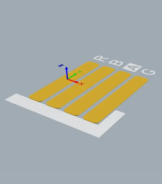
フットプリントは、最終的に基板のどちら側に配置されるかに関係なく、常にトップ面上に作成され、PCBエディタで使用できるものと同じツールおよび設計オブジェクト群を使用します。表面実装パッドやソルダーマスク定義などのレイヤー固有属性は、コンポーネント配置時にフットプリントを基板の反対側へ反転すると、自動的に適切なボトム側レイヤーへ転送されます。
設計オブジェクトは任意のレイヤーに配置できますが、通常、外形はTop Overlay(シルクスクリーン)レイヤー上に、パッドはマルチレイヤー(スルーホール部品のピン用)またはトップ信号レイヤー(表面実装部品のピン用)上に作成されます。フットプリントをPCB上に配置すると、フットプリントを構成するすべてのオブジェクトは、それぞれ定義されたレイヤーに割り当てられます。

ジョイスティックコンポーネント用フットプリントの2D表示と3D表示。3D画像には、そのコンポーネント用にインポートされたSTEPモデルが示されています。パッドとコンポーネントオーバーレイがSTEPモデルの下に見えている点に注意してください。
このページに示されているフットプリントは、必要な手順を説明するための例示にすぎず、寸法的に正確ではありません。新しいフットプリントは、必ずメーカーのデータシートと照合して仕様を確認してください。
コンポーネントフットプリントを手動で作成する一般的な手順は次のとおりです。
-
設計空間を準備する: スナップオプションを定義し、グリッドとガイドを設定します - 詳細はこちら。
-
フットプリントは、PCBフットプリント エディタ中央の設計空間基準点を中心に作成する必要があります。この基準点は実際には設計空間の相対原点であり、Place および Move 操作時にコンポーネントのフットプリントがカーソルでつかまれる位置になります(現在の Object Snap Options が PCB Editor – General ページの Preferences ダイアログでどのように設定されているかによります)。J, R ショートカットキーを使用すると、この基準点へ直接ジャンプできます。フットプリントの作成を始める前に基準点へ移動するのを忘れていた場合は、Edit » Set Reference サブメニューのコマンドを使用して基準パッドをフットプリントに取り込むことができます。
-
Pin 1 - コンポーネントの基準点を、そのコンポーネントフットプリントのピン1に設定します。
-
Center - コンポーネントの基準点を、コンポーネントフットプリントの中心に設定します。
-
Location - コンポーネントの基準点を、ユーザー定義の位置に設定します。
選択した点は 0,0 に設定されます。つまり新しい相対原点となり、すべてのプリミティブの位置はこの点を基準に更新されます。
-
コンポーネント要件に従って パッド (Place » Pad)を配置します。Place Pad コマンドを実行した後、最初のパッドを配置する前に Tab キーを押して Properties パネルを開き、パッドの Designator、Size and Shape、Layer、および(スルーホールパッドの場合の)Hole Size を含む、すべてのパッドプロパティを定義します。Designator は、後続のパッド配置時に自動的にインクリメントされます。表面実装パッドの場合は、Layer を Top Layer に設定します。スルーホールパッドの場合は、Layer を Multi-Layer に設定します。
-
新しいコンポーネントフットプリントを作成する際の最も重要な手順の1つは、コンポーネントを PCB にはんだ付けするために使用するパッドを配置することです。これらは、実際のデバイス上のピンに対応するよう、正確に正しい位置へ配置しなければなりません。
-
また、パッドの Designator を指定する際にも注意が必要です。というのも、回路図シンボル上のピン番号とのマッピングに Altium Designer が使用するのはこのプロパティだからです。
-
パッドを正確に配置するために、この作業専用のグリッドを設定することを検討してください。Ctrl+G ショートカットキーを使用して Cartesian Grid Editor dialog を開き、 Q キーでグリッドを Imperial から Metric に切り替えます。
-
マウスで移動しながらパッドを正確に配置するには、キーボードの矢印キーを使用して、現在のグリッド刻みでカーソルを移動します。さらに、Shift を押しながら操作すると、グリッドの10倍刻みで移動します。現在の X、Y 位置はステータスバーおよび Heads Up 表示にも表示されます。Heads Up Display には、位置情報に加えて、最後にクリックした位置から現在のカーソル位置までの差分も表示されます。Shift+H ショートカットを使用すると、Heads Up 表示のオン/オフを切り替えられます。あるいは、配置済みのパッドをダブルクリックして編集し、Properties パネルで必要な X および Y 位置を入力することもできます。
-
設計空間内の2点間の距離を確認するには、Reports » Measure Distance(ショートカット Ctrl+M)を使用します。ステータスバーの指示に従ってください。
-
ソルダーマスクやペーストマスクなどのパッド固有の属性は、パッド寸法と適用されるマスク設計ルールに基づいて自動計算されます。各パッドに対してマスク設定を手動で定義することもできますが、そうすると後で基板設計プロセス中にこれらの設定を変更しにくくなります。通常、これは設計ルールでパッドを対象指定できない場合にのみ行います。なお、ルールは基板設計時に PCB エディタ で定義されます。
-
Top Overlay レイヤー上で、トラック、アーク、その他のプリミティブオブジェクトを使用して、PCB シルクスクリーンに表示されるコンポーネント外形を定義します。配置時にコンポーネントが基板の裏面へ反転された場合、オーバーレイは自動的に Bottom Overlay レイヤーへ移されます。
-
配置コートヤードなどの追加の機械的詳細を定義するには、メカニカルレイヤー上にトラックやその他のプリミティブオブジェクトを配置します。メカニカルレイヤーは汎用レイヤーです。これらのレイヤーの機能を割り当て、各フットプリントで一貫して使用する必要があります。
-
PCB に実装される物理コンポーネントの三次元形状を定義するには、3D Body objects を配置します。
-
Designator および Comment 文字列は、PCB 設計空間へ配置する際に、フットプリントの Overlay レイヤーへ自動的に追加されます。追加の Designator および Comment 文字列は、メカニカルレイヤー上に .Designator および .Comment の特殊文字列を配置することで含めることができます。
-
フットプリントのプロパティ(名前や説明など)は、Properties パネルの Library Options モード(設計空間でオブジェクトが何も選択されていないときに有効で、メインメニューの Tools » Footprint Properties コマンドからアクセス可能)にある Footprint タブで定義します。パネルの Footprint タブで使用できるオプションやコントロールの詳細については、以下の section below を参照してください。
-
すべてのフットプリントで標準化されたパッド/ビア定義を行うには、Pad/Via ライブラリ(*.PvLib)を Pad/Via 配置に使用できます。learn more。
-
PCB Footprint エディタには、フットプリント作成プロセスを迅速化するためのウィザードもいくつか用意されています。
-
IPC Compliant Footprint Wizard – は、IPC standard 7351 – Generic Requirements for Surface Mount Design and Land Pattern Standard – Revision B に真に準拠した PCB フットプリントを生成します。learn more。
-
IPC Compliant Footprints Batch Generator – は、file-based PCB footprint library を使用して作業する場合に、複数のフットプリントを複数の密度レベルで迅速に生成するために使用します。IPC Compliant Footprints Batch Generator – learn more。
-
Footprint Wizard は、さまざまなパッケージタイプから選択して適切な情報を入力すると、コンポーネントフットプリントを作成してくれます。learn more。
設計空間の準備
デフォルトでは、グリッドはドットで表示されます。必要に応じて、グリッドを線で表示することもできます。これは Grid Editor ダイアログで設定します。このダイアログは、下の画像に示すように Properties パネルの Properties ボタンをクリックして開くことができます。あるいは、Ctrl+G ショートカットを押してダイアログを開きます。

画像では、細かいグリッドはドットで表示され、粗いグリッドは線で表示されています。
Properties Panel
PCB フットプリントエディタでフットプリントを編集していて、設計空間で現在どのデザインオブジェクトも選択されていない場合、Properties パネルには Library Options が表示されます。
以下の折りたたみ可能なセクションには、パネルの General タブで使用できるオプションとコントロールに関する情報が含まれています。
Selection Filter
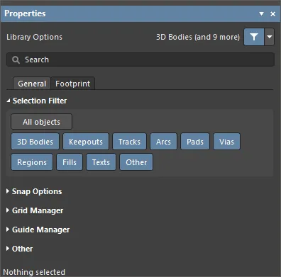
このパネルセクションのオプションは、設計空間で選択可能な PCB フットプリントオブジェクトを決定します。
-
All Objects button – オブジェクトフィルタリングを解除し、すべての種類のオブジェクトを選択可能にします。
-
Object buttons – 各オブジェクトボタンを切り替えて、そのオブジェクトタイプを選択できるかどうかを有効/無効にします。
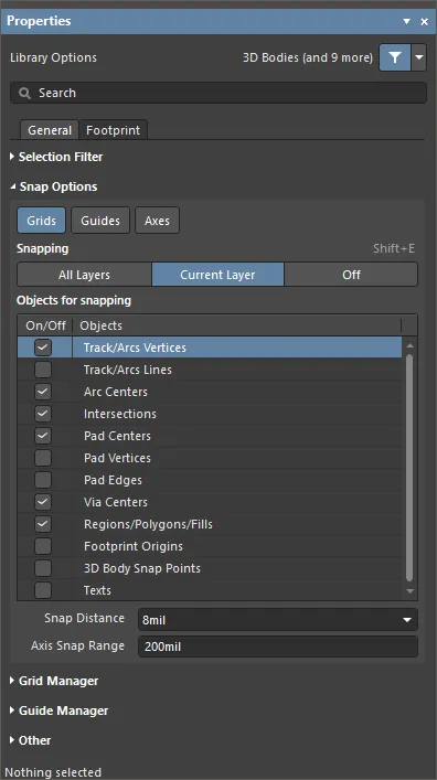
Snap Options
-
Grids – カーソルをアクティブな設計空間グリッドにスナップさせるかどうかを切り替えるために使用します。このオプションを有効にすると、カーソルは最も近いスナップグリッド位置へ引き寄せられます。アクティブなスナップグリッドは、ステータスバーおよび PCB エディタの Heads Up 表示(オン/オフ切り替えショートカットは Shift+H)に表示されます。
-
Guides – 手動で配置した線形またはポイント Snap Guide にカーソルをスナップさせるかどうかを切り替えるために使用します。Snap Guide は Snap Grid より優先されます。
-
Axes – 有効なスナップ対象オブジェクトに対して、カーソルを軸方向(X または Y 方向)に整列させるかどうかを切り替えるために使用します。Axis Snap Range は、X または Y の軸整列が発生する距離を定義します。現在のカーソル位置から、軸整列したオブジェクトのスナップポイント(ホットスポット)まで、整列が達成されると動的な整列ガイドラインが表示されます。
-
Snapping – 直接選択するか、Shift+E ショートカットを使用して、どのオブジェクト上でスナップするかを選択します。
-
All Layers – このオプションを有効にすると、任意の表示レイヤー上のすべての電気的オブジェクトにカーソルをスナップできるようになります。
-
Current Layer – このオプションを有効にすると、現在選択されているレイヤー上に配置されたオブジェクトのみを認識してスナップするようになります。
-
Off – このオプションを有効にすると、ホットスポットへのスナップを無効にします。
-
Objects for snapping
-
On/Off – 目的のオブジェクトに対するスナップを有効にするにはチェックします。
-
Objects – 使用可能なオブジェクトの一覧です。
-
Snap Distance – カーソルが有効なオブジェクトのスナップポイントからこの距離内に入ると(かつアクティブレイヤーでスナップが有効な場合)、カーソルはその点にスナップします。
-
Axis Snap Range – カーソルが有効なオブジェクト スナップ ポイントと軸方向に整列し、かつそのポイントからこの距離内にある場合(さらに Axes ボタンが有効な場合)、整列が達成されたことを示す動的ガイドラインが表示されます。
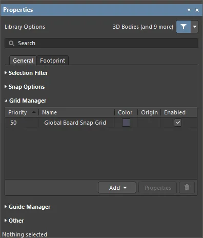
Grid Manager
-
Grid Manager – ボード用のデフォルト Snap Grid に加えて、ローカルにカスタマイズしたグリッドを定義および管理できます。
-
Priority – デザイン スペースでは、優先度は描画順で区別されます。最も優先度の高いグリッド(優先度
1)が他のすべてのグリッドの前面に描画され、次に優先度レベル 2 のグリッド、という順で続き、最後にデフォルト Global Board Snap Grid が他のすべてのカスタム グリッドの背面に描画されます。
-
Name – グリッドの名前を表示します。
-
Color – クリックするとドロップダウンが開き、関連付けられたグリッドの色を設定または変更できます。
-
Enabled – チェックすると、関連付けられたグリッドを有効にします。
-
Add
-
Add Cartesian Grid – クリックして直交グリッドを追加します。
-
Add Polar Grid – クリックして極座標グリッドを追加します。極座標グリッドを使用すると、非矩形のフィーチャやボードをより簡単に設計できます。
-
Properties – クリックすると、対応するグリッド エディタ ダイアログ(Cartesian Grid Editor または Polar Grid Editor)が開き、選択したグリッドのプロパティを変更できます。
-
 – クリックして現在選択されているグリッドを削除します。
Guide Manager
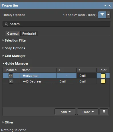
-
Guide Manager – ボード用の各種手動 Snap Guide および Snap Point を定義および管理できます。
-
Add – クリックして新しいスナップ ガイドまたはスナップ ポイントを追加します。関連メニューから必要なガイド タイプに対応するコマンドを選択すると、新しいガイド/ポイントのエントリがグリッドに追加されます。使用可能なガイド タイプは次のとおりです。
-
Add Horizontal Guide – このコマンドを使用して、デザイン スペース内の目的の Y 座標位置に水平ガイドラインを追加します。
-
Add Vertical Guide – このコマンドを使用して、デザイン スペース内の目的の X 座標位置に垂直ガイドラインを追加します。
-
Add +45 Guide – このコマンドを使用して、デザイン スペース内の目的の X,Y 座標位置を通る 45 度(y=x)のガイドラインを追加します。
-
Add -45 Guide – このコマンドを使用して、デザイン スペース内の目的の X,Y 座標位置を通る -45 度(y=-x)のガイドラインを追加します。
-
Add Snap Point – このコマンドを使用してポイント スナップ ガイドを追加します。これは、デフォルト スナップ グリッドの範囲内で手動でマークするホットスポットです。オブジェクトの配置や移動などのインタラクティブな処理中、オブジェクトのホットスポットがこのポイント スナップ ガイドに十分近づくと、そのポイントに「スナップ」します。
-
Place – クリックしてガイドを配置します。ドロップダウンからガイド タイプを選択します。
-
Place Horizontal Guide – このコマンドを使用して、デザイン スペース内の目的の Y 座標位置に水平ガイドラインを配置します。
-
Place Vertical Guide – このコマンドを使用して、デザイン スペース内の目的の X 座標位置に垂直ガイドラインを配置します。
-
Place +45 Guide – このコマンドを使用して、デザイン スペース内の目的の X,Y 座標位置を通る 45 度(y=x)のガイドラインを配置します。
-
Place -45 Guide – このコマンドを使用して、デザイン スペース内の目的の X,Y 座標位置を通る -45 度(y=-x)のガイドラインを配置します。
-
Place Snap Point – このコマンドを使用してポイント スナップ ガイドを配置します。これは、デフォルト スナップ グリッドの範囲内で手動でマークするホットスポットです。オブジェクトの配置や移動などのインタラクティブな処理中、オブジェクトのホットスポットがこのポイント スナップ ガイドに十分近づくと、そのポイントに「スナップ」します。
-
– クリックして現在選択されているガイドを削除します。
Other
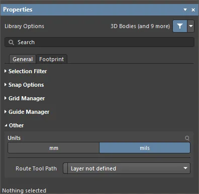
-
Units – 現在の PCB フットプリント ドキュメントのデフォルト測定単位を選択するために使用します。デフォルト単位は、画面上またはレポート内の距離関連情報の表示に使用されます。距離関連情報を指定する際に単位の接尾辞(mm または mil)が入力されていない場合は、常にデフォルト単位が使用されます。
-
Route Tool Path – ドロップダウンを使用して、ボードのルート ツール パスを定義する機械レイヤー(現在デザインで使用可能として有効になっているものの中から)を選択します。
以下の折りたたみ可能なセクションには、パネルの Footprint タブで使用できるオプションとコントロールに関する情報が含まれています。
Footprint パネルの Properties タブを使用してフットプリント プロパティを定義する機能は、Advanced Settings dialog で PCB.FootprintParameters オプションが有効になっている場合に利用できます。このオプションが無効な場合、フットプリント プロパティは PCB Library Footprint ダイアログ( )を使用して定義します。このダイアログには、メイン メニューから Tools » Footprint Properties コマンドを選択するか、PCB Library パネルの Footprints 領域でフットプリント エントリを選択して Edit ボタンをクリックするか、または PCB Library パネルの Footprints 領域でフットプリント エントリをダブルクリックすることでアクセスできます。
設計オブジェクトが選択されると、パネルにはそのオブジェクト種別に固有のオプションが表示されます。次の表は、PCBフットプリント設計空間内に配置可能なオブジェクト種別を示しています。リンクをクリックすると、そのオブジェクトのプロパティページにアクセスできます。
はんだマスクおよびペーストマスクの拡張
PCBフットプリントエディタで、はんだマスクおよび/またはペーストマスクが正しく定義されていることを確認するには、View Configuration panelを開き、各マスクレイヤーの表示オプション( )を有効にします。
各パッドの外周に Top Solder Mask レイヤーの色で表示されるリングは、マルチレイヤーパッドの下から拡張量分だけはみ出したはんだマスク形状の端を表しています。これは multi-layer がレイヤー描画順の最上位にあり、最前面に描画されるためです。Layer Drawing Order は PCB Editor - Display page(Preferences ダイアログ内)で設定します。
下の画像は、各パッドの外周に紫色(Top Solder Mask レイヤーの色)の境界が表示された PCB フットプリントを示しています。

レイヤーをすばやく切り替えて確認するには、Single Layer Mode(Shift+S)を Ctrl+Shift+Wheel roll と組み合わせて使用します。
デフォルトでは、マスクレイヤー上に作成される形状はパッド形状であり、フットプリントが配置される PCB 上で設定された Solder Mask Expansion および Paste Mask Expansion デザインルールで指定された量だけ拡張または縮小されます。場合によっては、拡張デザインルールを上書きして、マスク拡張をパッド属性として指定したり、あらかじめ定義された標準マスク形状セットから選択したり、独自のカスタム形状を作成したりする必要があります。このような場合、選択したパッドの Properties panel - learn more でペースト/はんだマスクを設定できます。あるいは、必要なマスクレイヤー上に適切なプリミティブ(Region、Track など)を配置することもできます。
PCB ライブラリでは、ルール駆動のはんだマスク拡張を持つすべてのオブジェクトの拡張値は 0 mil になります。この機能は、PCB.SolderMaskZeroExpansion オプションが Advanced Settings dialog で有効になっている場合に利用できます。このオプションが無効な場合、PCB ライブラリ内のそのようなオブジェクトのはんだマスク拡張値は 4 mil になります。
パラメータのサポート
Altium Designer でオブジェクトに適用されるパラメータは、PCB 設計に追加情報を付加するための強力かつ柔軟な手段を提供します。親オブジェクトのプロパティとして適用されるパラメータは、プロジェクト、ドキュメント、テンプレート、設計ドキュメント内の個々のオブジェクトなど、さまざまなレベルで適用できます。
PCB 空間で利用可能になったパラメータは、クエリ、デザインルール、スクリプト、バリアントのフィルタリングに使用でき、配置済みフットプリント内でカスタム文字列を呼び出すために PCB コンポーネントフットプリントにも適用できます。
Engineering Change Order によるパラメータ
PCB パラメータ機能は、ECO メカニズムおよび PCB ドキュメントに含まれる機能に基づいており、ユーザー定義のコンポーネントパラメータを PCB 空間へ転送して保持できます。これは一方向の転送であり、転送されたパラメータは PCB ドメインでは読み取り専用です。
パラメータの転送は、回路図から PCB へ Design » Update PCB Document メニューコマンドを使用して ECO を作成することで行われます。

ECO が実行されると(Execute Changes ボタンを使用)、新しいユーザー定義の回路図コンポーネントパラメータが、PCB 設計内の対応するフットプリント参照へ転送されます。
PCB へのパラメータの検出と移行は、プロジェクトのオプション設定(Project » Project Options)によって決まります。Project Options ダイアログでは、Comparator タブの Differences Associated with Parameters セクションと、 ECO Generation タブの Modifications Associated with Parameters セクションで、差分検出および変更動作を設定します。
PCB エディタで転送されたパラメータを表示するには、コンポーネントをダブルクリックして Properties パネルを開き、Parameters タブを選択します。このタブには、選択したコンポーネントフットプリントに割り当てられている現在のユーザーパラメータが一覧表示されます。選択したコンポーネントフットプリントのパラメータは、Components パネルでも利用できます。
情報参照リンク
PCB ドメインは、回路図から事前定義された ComponentLink パラメータを自動的に受け入れます。これらはパラメータのペア(説明とリンク URL)として定義され、通常は特定のファイルやインターネット上の場所へのデータ参照リンクを確立します。一般的には、メーカーの Web サイトやデータシート URL です。
回路図および PCB の両方の設計空間で、リンクはコンポーネント上にマウスオーバーした際の右クリックコンテキストメニュー(References サブメニューオプション内)からアクセスします。これらの専用パラメータは Properties パネルで追加され、PCB 空間へ転送されるとコンポーネントフットプリントパラメータとして表示されます。

ソースフットプリント内のパラメータ
PCB に渡されたパラメータは、コンポーネントフットプリントを通じて基板製造や機能に関する追加情報を提供するために使用できます。ソースライブラリレベルでフットプリントに特別なパラメータ文字列を追加することで、カスタム文字列が対象のメカニカルレイヤーまたはオーバーレイ上で解釈されます。
ユーザー定義パラメータを表す特別な文字列は、Properties パネル内の special strings ボタンとドロップダウン( )を使用して、ソースコンポーネントフットプリントに追加できます。

下のライブラリフットプリントでは、特別な文字列 .Designator が Mechanical 2 レイヤー上に配置されています。

ユーザーパラメータを表す特別な文字列は、コンポーネントフットプリントに追加できます。
そのカスタムパラメータが回路図コンポーネントにも適用され、パラメータデータが PCB に転送されると、解釈されたフットプリント文字列が基板ビューと生成出力ファイルの両方に表示されます。この場合、特別なパラメータ文字列には、実装を支援するためのカスタムコンポーネント部品識別子が含まれています。
特別な文字列としてコンポーネントフットプリントにユーザーパラメータを適用することで、スイッチやコネクタの機能ラベルなど、その他さまざまなカスタム PCB 要件にも対応できます。たとえば、その種のコンポーネントのフットプリントでは、「function」パラメータ文字列を Top Overlay に配置できます。
基板レイアウト上で特別な文字列の解釈後の値を表示するには、View Configuration パネルの View Options タブにある Additional Options 領域で Special Strings オプションを有効にします。特別な文字列は、生成出力ファイルでは常に変換されます。
回路図エディタでは、必要に応じて Preferences ダイアログの Schematic – Graphical Editing ページで Display Names of Special Strings that have No Value Defined オプションを有効にします。
パラメータクエリ
PCB ドメイン内のパラメータ文字列は Altium Designer のクエリ言語からもアクセス可能であり、そのため Find Similar Objects 機能を含むオブジェクトフィルタリング機能で利用できます。
類似オブジェクトの選択を実行するには、コンポーネントを右クリックし、コンテキストメニューから Find Similar Objects を選択して Find Similar Objects ダイアログを開きます。

Find Similar Objects dialog には Parameters セクションがあり、必要に応じてフィルタリングオプションを選択できます。

PCB Filter パネルでは、パラメータ固有のクエリワードをフィルタ条件として適用でき、PCB パラメータに基づくデザインルールの作成にも使用できます。
PCB フットプリントパラメータを扱うためのクエリワードがいくつか用意されており、文字列値を数値に変換するための専用関数ワード(たとえば StrToNumber)も含まれます。文字列 Value の変換は単位認識型(V、mA、mV、kOhm など)であり、パラメータ値文字列の数値処理によってクエリ結果を判定できます。
クエリで指定可能なサポート対象の単位タイプは次のとおりです。
-
% – パーセント
-
A – 電流
-
C – 温度
-
dB – デシベル
-
F – 静電容量
-
G – コンダクタンス
-
H – インダクタンス
-
Hz – 周波数
-
Kg – 質量
-
m – 長さ
-
Ohm – 抵抗
-
Q – 電荷
-
s – 時間
-
V – 電圧
-
W – 電力
-
Z – インピーダンス

PCB コンポーネントフットプリントパラメータを扱うための Parameter クエリワードがいくつか用意されています。
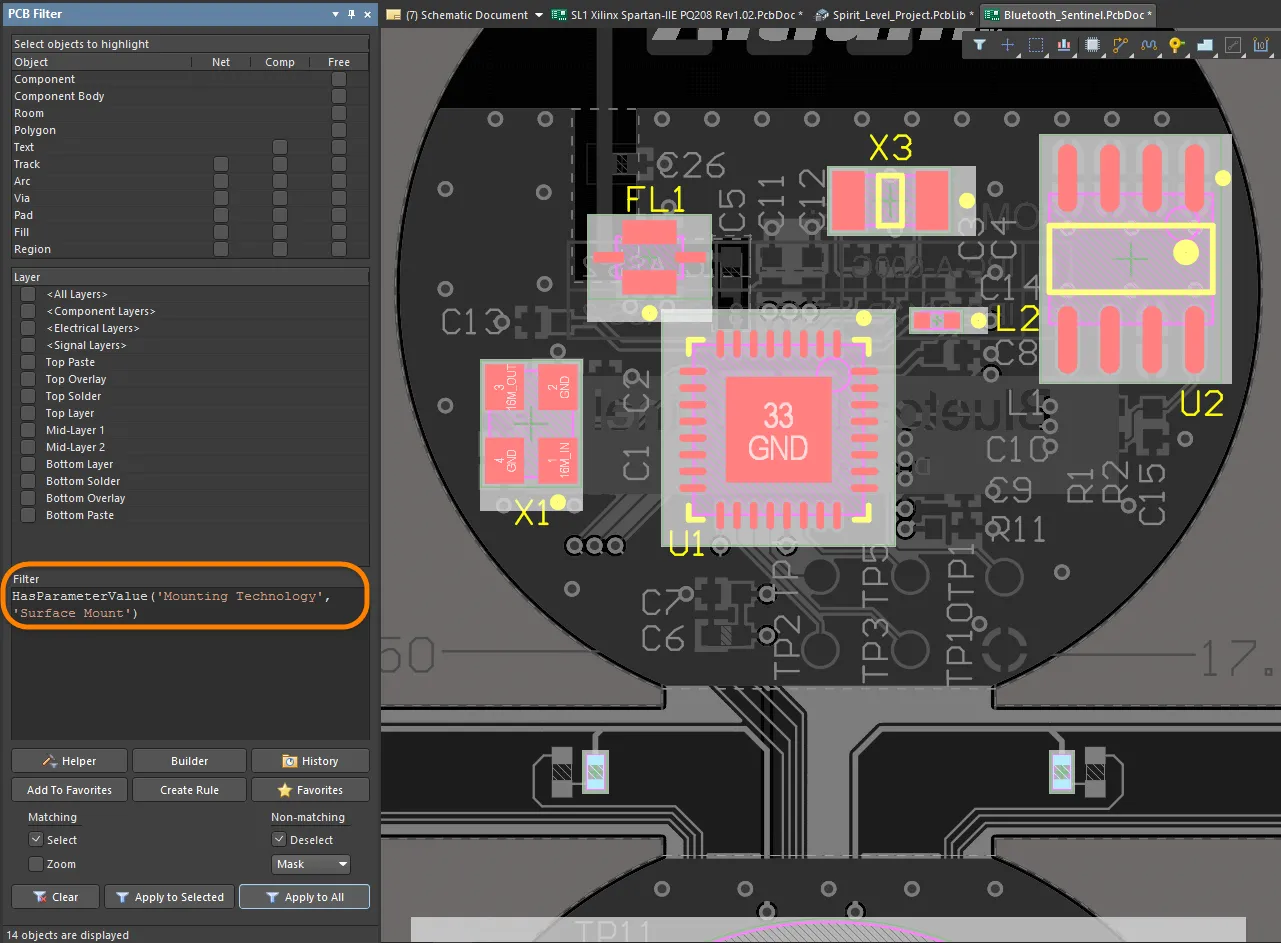
上の Query Helper ダイアログに示された例では、各コンポーネントの Voltage Rating パラメータを処理し(文字列から数値への変換 StrToNumber(Unit Value, Unit Type) を使用)、その値が 50V を超えるかどうかを判定しています。これを PCB Filter パネルに適用すると、例の基板レイアウトでは高電圧コンポーネントが 1 つ表示されます。C1 ( の Voltage Rating 値は 3kV です)。
Scientific E表記もサポートされているため、たとえば1nFを超えるコンデンサ値をフィルタリングするクエリは、次のようになります。
StrToNumber(ParameterValue('CapacitanceValue'), F) > 1e-9
あるいは、返されるParameterValue and 比較値の両方に対して、数値変換関数を使用することもできます。
StrToNumber(ParameterValue('CapacitanceValue'), F) > StrToNumber('1nF', F)
ルールとスクリプト
PCBパラメータクエリは、Altium Designerのスクリプトおよびデザインルールにも適用できます。後者では、たとえばフットプリントパラメータを検出して部品配置やレイヤ割り当てを評価するなど、レイアウト検証チェックを実行できます。なお、上記の Query Helper ダイアログに示されている関数は、スクリプト言語でも使用できます。
以下の例では、コンデンサの定格電圧クエリ(上記のフィルタクエリを参照)を部品配置ルールに適用しており、実行時に高電圧(>50V)デバイスとして検出された部品に対して、特定のクリアランス値をチェックします。

回路図空間から転送された特定のフットプリントパラメータによって定義されたデザインルールは、カスタムなレイアウト条件の検出に使用できます。
同様に、カスタムPCBパラメータを使用して部品のレイヤ互換性をチェックすることもできます。たとえば、ある部品がウェーブはんだ付けに対応しておらず、そのためBottom Layerへの配置をサポートしない場合です。ここでは、カスタムの「WaveSoldering」パラメータ(Yes/No)を処理するオブジェクト一致クエリを、 Permitted Layers Ruleに適用できます。

その後、この(バッチ)ルールはその部品パラメータの値をチェックし、部品がBottom Layerへの配置に適合しない場合は違反を生成します。
バリアント
PCBに転送されたパラメータのうち、設計のバリエーション(Design Variants)に含まれるものは、バリアント選択によって処理されます。
実際には、PCB空間内のバリアント化された部品パラメータは、クエリ文字列によって動的に検出されたり、たとえば特殊文字列を介して基板レイヤに表示されたりします。
ユーザー定義フットプリントパラメータ
フットプリントのユーザー定義パラメータは、Altium Designerでサポートされています。PCBフットプリントエディタのデザイン空間でオブジェクトが選択されていない場合、 Properties パネルの Library Options モードにある Footprint タブ上の Parameters 領域を使用して、フットプリントパラメータの表示および編集を行えます。

部品がPCB上に配置されると、 Properties パネルの Component モードの Parameters タブで、これらのパラメータを確認できます。
-
PCB上に配置された部品のフットプリントパラメータは、PCBエディタのメインメニューにある Make PCB Library または Make Integrated Library コマンドによって生成されるライブラリ内のフットプリントにも反映されます。
-
フットプリントパラメータは、Altium Designerの比較エンジン、および生成されるPick and Place出力とODB++出力でサポートされています。
Designator文字列とComment文字列
デフォルトのDesignator文字列とComment文字列
フットプリントが基板上に配置されると、設計の回路図ビューから抽出された情報に基づいてDesignatorとCommentが与えられます。Designator文字列およびComment文字列のプレースホルダは、フットプリントが基板上に配置される際に自動的に追加されるため、手動で定義する必要はありません。これらの文字列の位置は、デザイン空間でdesignatorまたはcomment文字列を選択したときの Parameter モードにおける Properties パネル内のDesignator文字列およびComment文字列の Autoposition オプションによって決まります。Designator文字列とComment文字列のデフォルトの位置およびサイズは、Preferences ダイアログの PCB Editor - Defaults page にあるそれぞれのPrimitiveで設定します。

追加のDesignator文字列とComment文字列
Designator文字列またはComment文字列の追加コピーが必要になる場合があります。たとえば、実装委託先が、各部品外形の内側にDesignatorが表示された詳細な組立図を求める一方で、自社では最終PCBの部品オーバーレイ上で部品のすぐ上にDesignatorを配置することを要求する場合です。この追加のDesignator要件は、フットプリントに .Designator 特殊文字列を含めることで実現できます。Comment文字列の位置を別のレイヤや場所に指定するための .Comment 特殊文字列も用意されています。
実装委託先の要件に対応するには、PCBフットプリントエディタの機械レイヤに .Designator 文字列を配置し、このレイヤを含む印刷出力を設計組立指示の一部として生成します。
レイヤ固有の特別な要件への対応
PCB部品には、接着剤ドットや剥離可能なソルダーマスク定義が必要になるなど、さまざまな特別要件が存在します。これらの特別要件の多くは、部品が実装される基板面に関連しており、部品が反転されたときには基板の反対面へ移る必要があります。
めったに使用されない可能性のある特殊用途レイヤを多数用意する代わりに、Altium DesignerのPCBエディタでは、レイヤペアと呼ばれる機能によってこの要件をサポートしています。レイヤペアとは、ペアとして定義された2つの機械レイヤです。部品が基板の片面から反対面へ反転されると、ペアになっている機械レイヤ上のすべてのオブジェクトは、そのペアのもう一方の機械レイヤへ反転されます。 この方法では、接着剤ドット(またはその他の特別要件)を含めるのに適した機械レイヤを選択し、利用可能なオブジェクトを使ってその形状を定義します。 そのフットプリントを基板上に配置したら、レイヤペアリングを設定する必要があります。これにより、この部品が基板の反対面へ反転されたときに、どのレイヤへオブジェクトを移すべきかがソフトウェアに指示されます。PCBフットプリントエディタではレイヤペアを定義できず、これはPCBエディタで行います。
レイヤペアリングは、部品を反転するbefore前に定義しておく必要があります。部品が下面側へ移動した後でペアリングを定義すると、機械レイヤの内容は反転しますが、元のレイヤにとどまります。反転前にレイヤペアを作成し忘れた場合は、ライブラリから更新して、基板上に配置されたその部品インスタンスをリフレッシュできます。
Mechanical Layersの名前は、View Configurations パネル上で右クリックし、Edit Layer を選択することで直接編集できます。
機械レイヤの使用を管理する一般的な方法は、必要な各機械レイヤ機能に対して専用のレイヤ番号を割り当てることです。この方法では、すべての設計者が同じレイヤ割り当ておよび番号付けスキームに従う必要があります。また、同じ割り当ておよび番号付けスキームに従っていない他のソースから部品を入手した場合に問題が生じることがあります。異なるスキームが使用されている場合、その設計オブジェクトを現在の機械レイヤから、その機能に割り当てられた機械レイヤへ移動しなければなりません。
この問題は、Layer Type プロパティの導入によって解決されます。部品がライブラリからPCBエディタに配置された場合、あるいはあるライブラリから別のライブラリへコピーされた場合、または IPC Footprint Wizard によって作成された場合、既存のLayer Type割り当ては、これらのLayer Typeに割り当てられた機械レイヤ番号に関係なく、自動的に一致付けされます。オブジェクトは、そのLayer Typeに従って正しいレイヤへ再配置されます。ソフトウェアがLayer Typeによる一致付けを行えない場合は、Layer Numberによる一致付けにフォールバックします。
個別の機械レイヤとComponent Layer Pairsの両方について、定義済みタイプのリストからLayer Typeを選択できます。以下に示すダイアログには、個別のレイヤを右クリックし、メニューから Edit Layer または Add Component Layer コマンドを選択することでアクセスできます。
PCBフットプリントへの高さの追加
3D表現の最も基本的なレベルでは、高さ情報をPCBフットプリントに追加できます。これを行うには、Properties パネルを Library Options モードで開き(デザイン空間でオブジェクトが選択されていないときに有効)、パネルの Footprint タブにある Height フィールドに、その部品の推奨高さを入力します。
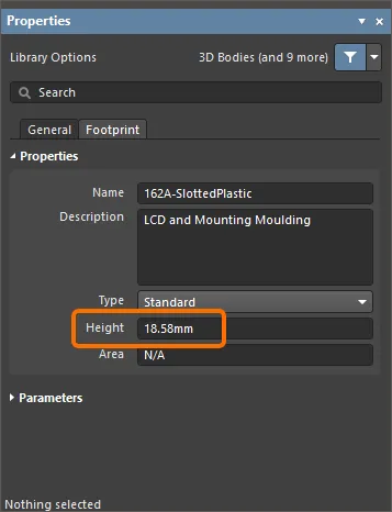
高さに関するデザインルールは、基板設計中に定義できます(PCB Editorで Design » Rules をクリック)。通常は、部品クラス内またはルーム定義内での最大部品高さをチェックします。
高さ情報を定義するより良い方法は、PCBフットプリントに 3D Bodies を追加することです。
配線プリミティブを持つ部品の管理
設計が転送されると、各部品で指定されたフットプリントが利用可能なライブラリから抽出され、基板上に配置されます。次に、フットプリント内の各パッドのnetプロパティは、回路図内でその部品ピンに接続されているネット名に設定されます。パッドに接触しているすべてのオブジェクトは、そのパッドと同じネットに接続されます。
PCBエディタには、包括的なネット管理ツールが含まれています。起動するには、メインメニューから Design » Netlist » Configure Physical Nets を選択して Configure Physical Nets dialog を開きます。オプションメニューを表示するには Menu ボタンをクリックします。未割り当てのプリミティブに割り当てるネットを選択するには、New Net Name ヘッダーのドロップダウンをクリックします。

同じピンに接続された複数のパッドを持つフットプリント
以下に示すフットプリントは SOT223 トランジスタで、同じ論理回路図コンポーネントのピン、つまり Pin 2 に接続された複数のパッドを持っています。この接続を実現するために、同じデジグネータ「2」を持つ 2 つのパッドが追加されています。 Schematic Editor で Design » Update PCB コマンドを使用して設計情報を PCB に転送すると、同期結果では PCB エディター上で両方のパッドに接続線が表示されます。つまり、これらは同じネット上にあります。どちらも配線可能です。

デジグネータ 2 のパッドが 2 つある SOT223 フットプリント。
シルクスクリーンの準備
露出銅箔や穴にシルクスクリーンが重なることで発生する一般的な Design for Manufacture (DFM) の問題を解決しやすくするため、PCB フットプリントエディターには、フットプリント用のシルクスクリーンを準備する専用機能が用意されています。これらの問題には、次の方法で効果的に対処できます。
-
シルクスクリーンの線分および円弧の自動クリッピング
-
塗りつぶしおよびリージョンの自動クリッピングまたは移動
-
シルクスクリーンのテキスト文字列の自動移動
PCB の設計中にもシルクスクリーン準備ツールにアクセスできます。
詳細はこちら。
PCB フットプリントエディターでシルクスクリーン準備ツールにアクセスするには、メインメニューから Tools » Silkscreen Preparation コマンドを使用します。Silkscreen Preparation ダイアログが開きます。

このダイアログを使用して、シルクスクリーンオブジェクトのクリッピング/移動設定を構成します。使用可能なオプションは次のとおりです。
-
Clip to Exposed Copper – 有効にすると、露出銅箔に対してオブジェクトを自動的にクリッピングします。
-
Clip to Solder Mask Openings – 有効にすると、ソルダーマスク開口部に対してオブジェクトを自動的にクリッピングします。
-
Silkscreen Clearance – シルクスクリーンオブジェクトと露出銅箔/ソルダーマスク開口部および穴との間の最小許容値を定義します。
-
Min Remaining Length – クリッピング後の線分/円弧の長さが定義値未満の場合、そのオブジェクトはフットプリントから削除されます。この長さはエッジ間の長さではなく、頂点間の長さである点に注意してください。 –
![]() 画像を表示。
画像を表示。
-
Move Text – 露出銅箔/ソルダーマスク開口部および穴との距離が Silkscreen Clearance 未満の場合、シルクスクリーンのテキスト文字列をそれらから離すように移動します。移動量は Max Distance 値によって制限されます。
-
Fill & Region – 塗りつぶしおよびリージョンと露出銅箔/ソルダーマスク開口部および穴との距離が Silkscreen Clearance 未満の場合に実行するアクションを選択します。
-
None – 塗りつぶしおよびリージョンは変更されません。
-
Clip – 塗りつぶしおよびリージョンは Silkscreen Clearance を維持するようにクリッピングされます。必要に応じて、塗りつぶしはリージョンに変換されます。
-
Move – 塗りつぶしおよびリージョンは、露出銅箔/ソルダーマスク開口部および穴から離れるように移動されます。移動量は Max Distance 値によって制限されます。
-
Max Distance – テキスト文字列、コンポーネントデジグネータ、塗りつぶし、およびリージョンを Silkscreen Clearance を維持するために移動できる最大距離を定義します。
OK をクリックすると、ダイアログの設定に従ってシルクスクリーンオブジェクトのクリッピングおよび/または移動が実行されます。
オブジェクトに対してアクションを実行できない場合(たとえば、Max Distance の制限によりテキスト文字列を移動できない場合)、そのオブジェクトに関するメッセージが Messages パネルに表示されます。
シルクスクリーン準備ツールの動作例を以下に示します。
IPC 準拠フットプリントウィザードを使用したフットプリントの作成
IPC Compliant Footprint Wizard は、IPC 規格 7351 Revision B(Generic Requirements for Surface Mount Design and Land Pattern Standard)に真に準拠した PCB フットプリントを生成します。Footprint Wizard のようにフットプリント寸法を直接扱うのではなく、IPC Compliant Footprint Wizard はコンポーネント自体の寸法情報を使用し、IPC が公開したアルゴリズムに従って適切なパッドおよびその他のフットプリント特性を計算します。
フットプリントを定義するために使用されるパッドやトラックのプロパティを入力する代わりに、Wizard は実際のコンポーネント寸法を入力値として受け取ります。IPC-7351 規格向けに開発された数式に基づき、Wizard はパッドやトラックなどの標準的な Altium Designer オブジェクトを使用してフットプリントを生成します。
このダイアログは、IPC 規格 7351 Revision B(Generic Requirements for Surface Mount Design and Land Pattern Standard)に準拠しています。IPC-7351B は 2010 年にリリースされ、2007 年にリリースされた IPC-7351A に代わるものです。

Altium Designer で IPC Compliant Footprint Wizard にアクセスするには、IPC Footprint Generator ソフトウェア拡張機能がインストールされている必要があります。 この拡張機能は、デフォルトで Altium Designer にインストールされています。 手動でインストールまたは削除することもできます。
拡張機能の管理の詳細については、Extending Your Installation ページ(Altium Designer Develop、Altium Designer Agile、Altium Designer)を参照してください。
IPC Compliant Footprint Wizard を実行するには、メインメニューから Tools » IPC Compliant Footprint Wizard を選択します。
Select Component Type ページで、Select Component Type ページ上にフットプリントを作成したいコンポーネントファミリを選択します。ウィザード右側のプレビュー領域は動的に変化し、現在選択されているコンポーネントを表示するとともに、生成可能なパッケージの種類も示します。以下の表に、ウィザードでサポートされているコンポーネントタイプとパッケージを示します。
| 名前 |
説明 |
含まれるパッケージ |
| BGA |
ボールグリッドアレイ |
BGA, CGA |
| BQFP |
バンパード・クワッド・フラット・パック |
BQFP |
| CAPAE |
電解アルミニウムコンデンサ |
CAPAE |
| CFP |
セラミック・デュアル・フラット・パック - トリミングおよび成形済みガルウィングリード |
CFP |
| Chip Array |
チップアレイ |
Chip Array |
| DFN |
デュアル・フラット・ノーリード |
DFN |
| CHIP |
2 ピンのチップ部品 |
コンデンサ、インダクタ、抵抗 |
| CQFP |
セラミック・クワッド・フラット・パック - トリミングおよび成形済みガルウィングリード |
CQFP |
| DPAK |
トランジスタアウトライン |
DPAK |
| LCC |
リードレス・チップ・キャリア |
LCC |
| LGA |
ランドグリッドアレイ |
LGA |
| MELF |
2 ピンの MELF 部品 |
ダイオード、抵抗 |
| MOLDED |
2 ピンのモールド部品 |
コンデンサ、インダクタ、ダイオード |
| PLCC |
プラスチック・リーデッド・チップ・キャリア、正方形 - J リード |
PLCC |
| PQFN |
プルバック・クワッド・フラット・ノーリード |
PQFN |
| PQFP |
プラスチック・クワッド・フラット・パック |
PQFP, PQFP Exposed Pad |
| PSON |
プルバック・スモール・アウトライン・ノーリード |
PSON |
| QFN |
クワッド・フラット・ノーリード |
QFN, LLP |
| QFN-2ROW |
クワッド・フラット・ノーリード、2 列、正方形 |
ダブルロウ QFN |
| SODFL |
スモール・アウトライン・ダイオード、フラットリード |
SODFL |
| SOIC |
スモール・アウトライン集積回路パッケージ、1.27mm ピッチ - ガルウィングリード |
SOIC, SOIC Exposed Pad |
| SOJ |
スモール・アウトライン・パッケージ - J リード |
SOJ |
| SON |
スモール・アウトライン・ノンリード |
SON, SON Exposed Pad |
| SOP, TSOP |
スモール・アウトライン・パッケージ - ガルウィングリード |
SOP, TSOP, TSSOP |
| SOT143/343 |
スモール・アウトライン・トランジスタ |
SOT143, SOT343 |
| SOT223 |
スモール・アウトライン・トランジスタ |
SOT223 |
| SOT23 |
スモール・アウトライン・トランジスタ |
3 リード、5 リード、6 リード |
| SOT89 |
スモール・アウトライン・トランジスタ |
SOT89 |
| SOTFL |
スモール・アウトライン・トランジスタ、フラットリード |
3 リード、5 リード、6 リード |
| WIRE WOUND |
高精度巻線インダクタ、2 ピン |
インダクタ |
ウィザードの後続ページは、選択したコンポーネントタイプに応じて変化します。直感的なウィザードページに従って、必要なコンポーネントフットプリントを設定してください。IPC Compliant Footprint Wizard を使用する際の注意点を以下に示します。
フットプリント Wizard を使用したフットプリントの作成
PCB フットプリントエディタには Footprint Wizard が含まれています。この Wizard では、さまざまなパッケージタイプから選択して適切な情報を入力すると、コンポーネントのフットプリントが自動的に作成されます。なお、Footprint Wizard では、パッドおよびコンポーネントオーバーレイに必要なサイズを入力します。

Footprint Wizard を起動するには、メインメニューから Tools » Footprint Wizard を選択するか、デザインスペース内で右クリックしてコンテキストメニューから Tools » Footprint Wizard コマンドを選択します。
Component patterns ページを使用して、作成したいコンポーネントのパターンを指定します。リストから目的のパターンを選択し、ドロップダウンを使用してコンポーネントの単位(Imperial (mil) または Metric (mm))を選択します。使用可能なパターンは次のとおりです。
-
Ball Grid Arrays (BGA)
-
Capacitors
-
Diodes
-
Dual In-line Packages (DIP)
-
Edge Connectors
-
Leadless Chip Carriers (LCC)
-
Pin Grid Arrays (PGA)
-
Quad Packs (QUAD)
-
Resistors
-
Small Outline Packages (SOP)
-
Staggered Ball Grid Arrays (SBGA)
-
Staggered Pin Grid Arrays (SPGA)
その後の Wizard のページは、選択したコンポーネントパターンに応じて変化します。必要なコンポーネントフットプリントを設定するために、Wizard の直感的なページに従って進めてください。
Edge Connectors、
Leadless Chip Carriers (LCC) または
Quad Packs (QUAD) パターンのフットプリントについてパッド命名スタイルを設定する際は、緑色の矢印をクリックして命名順序/方向を変更します。–
![]() show image
show image.
コンポーネントレポートの生成
アクティブな PCB フットプリントのレポートを生成するには、メインメニューから Reports » Component コマンドを選択します。 コマンドを起動すると、レポートはソース PCB ライブラリドキュメントと同じフォルダに生成され(<PCBLibraryDocumentName>.CMP)、メインデザインウィンドウでアクティブドキュメントとして自動的に開かれます。レポートには、フットプリント寸法、フットプリントを構成するプリミティブオブジェクトの内訳、およびそれらが存在するレイヤーなどの情報が一覧表示されます。
このレポートは、Projects パネルの Documentation\Text Documents サブフォルダの下に、フリードキュメントとして追加されます。

 AI で翻訳