部品が製造された基板上で占める領域は、部品のフットプリントによって定義されます。典型的なフットプリントにはパッドと部品のオーバーレイが含まれ、必要に応じてその他の機械的詳細も含まれることがあります。下の例のフットプリントでは、この部品が基板の切り欠き部分にまたがって取り付けられるため、部品のアウトラインのほとんどが(黄色の)オーバーレイではなく、機械層(緑色の線)上に定義されています。

フットプリントは、部品が占める空間を定義し、部品のピン/パッドから基板上の配線への接続点を提供します。
そのフットプリント上に取り付けられる部品は、3D Bodyオブジェクトを使用してモデル化することができます。3D Bodyオブジェクトは、下の画像に示されているように、汎用MCAD形式モデルをインポートするためのコンテナとして使用されます。

適切なMCADモデルを3D Bodyオブジェクトにインポートできます。
既製のPCB部品を提供する豊富なリソース(例えばManufacturer Part Search panelなど)があるにも関わらず、キャリアのある時点でカスタムPCB部品を作成する必要が生じる可能性が高いです。PCB部品のフットプリントは、PCBエディタで利用可能な同じプリミティブオブジェクトセットを使用してPCBフットプリントエディタで作成されます。フットプリントに加えて、会社のロゴ、製造定義、および基板設計中に必要とされるその他のオブジェクトもPCB部品として保存できます。
新しいPCBフットプリントの作成
フットプリントは、接続されたWorkspace内で直接作成できます。これを行うには:
-
メインメニューからFile » New » Libraryを選択し、開いたNew Libraryダイアログで、ダイアログのWorkspace 領域からCreate Library Content » Footprintを選択します。

New Libraryダイアログを使用して新しいWorkspaceフットプリントを作成します。
-
開いた新規アイテムの作成 ダイアログで、必要な情報を入力し、Open for editing after creationオプションが有効になっていることを確認してOK をクリックします。Workspaceフットプリントが作成され、一時的なPCBフットプリントエディタが開き、アクティブなドキュメントとして.PcbLib ドキュメントが表示されます。このドキュメントはアイテム-リビジョンに従って命名され、形式は <Item><Revision>.PcbLib (例: PCC-001-0001-1.PcbLib)となります。以下に説明するようにフットプリントを定義します。

Workspaceフットプリントの初期リビジョンを編集する例 – 一時的なPCBフットプリントエディタは、フットプリントを定義するためのドキュメントを提供します。
-
フットプリントが必要に応じて定義されたら、Save to Serverコントロールを使用してWorkspaceに保存します。これは、Projectsパネル内のフットプリントのエントリの右側にあります。Edit Revisionダイアログが表示され、必要に応じて名前、説明を変更し、リリースノートを追加できます。ドキュメントとエディタは保存後に閉じます。
保存されたWorkspaceフットプリントは、コンポーネントエディタを使用してコンポーネントを定義する際に、Single Component Editingモード またはBatch Component Editingモードで使用できます。
WorkspaceフットプリントはComponentsパネルを使用して閲覧できます。パネルの上部にある  ボタンをクリックしてモデルの表示を有効にし、Modelsを選択した後、Footprintsカテゴリを選択します。

Workspaceフットプリントを編集するには、コンポーネントパネルでそのエントリを右クリックし、Editコマンドを選択します。再び、一時的なエディタが開き、編集のためにフットプリントが開かれます。必要に応じて変更を加え、次のリビジョンのWorkspaceフットプリントとしてドキュメントを保存します。
関連するコンポーネントの更新
ワークスペースドメインモデル(シンボル、フットプリントモデル、シミュレーションモデルなど)に変更を加えると、その変更をモデルの新しいリビジョンに保存すると、そのモデルを使用するワークスペースコンポーネントは実質的に古くなり、以前のリビジョンが引き続き使用されます。ほとんどの場合、これらのワークスペースコンポーネントを再保存し、利用可能な最新のリビジョンを使用するようにそれぞれのモデルリンクを更新したいと思うでしょう。このプロセスを効率化するために、WorkspaceはAltium Designerと連携して、直接編集機能を通じてそのモデルに変更を加えた後、Workspaceモデルを再保存する時点で、関連するコンポーネントを更新する機能を容易にします。
親コンポーネントに対してこの更新を実行するオプションは、変更したワークスペースフットプリントをターゲットワークスペースに保存し直すときに表示されるCreate Revisionダイアログにあります。このオプション (Update items related to <ModelItemRevision> ) は、デフォルトで有効になっています。
<ModelItemRevision> は、モデルの現在のリビジョン、つまり、関連するワークスペースコンポーネントによって現在使用されているリビジョンです。Workspace モデル自体を保存すると、当然のことながら、これは以前の (以前の) リビジョンであり、最新のリビジョンではなくなります。

再保存されるワークスペースフットプリントを参照している関連するワークスペースコンポーネントを更新するオプションにアクセスする。
ワークスペースフットプリントの現在のリビジョンを使用してすべての関連コンポーネントを保持する場合は、このオプションを無効にします。その後、Workspace モデル自体のみが保存されます。
Create RevisionダイアログでOKをクリックすると、変更したフットプリントがワークスペースに保存され、関連する一時的なエディタが閉じます。そのワークスペースフットプリントを参照するすべてのワークスペースコンポーネントは、新しいリビジョンを自動的に使用するために再保存されます(各コンポーネントの次のリビジョンが自動的に作成され、保存が実行されます)。
-
デザイナーの視点から見ると、Workspace コンポーネントは、すべてのデザイン ドメインでそのコンポーネントを表すために必要なすべての情報を 1 つのエンティティにまとめます。したがって、この点では、すべてのドメインモデルとパラメトリック情報が格納される「バケット」であるコンテナと考えることができます。さまざまなドメインでの表現という点では、Workspace コンポーネントには Workspace ドメイン モデル自体は含まれず、これらのモデルへのリンクが含まれています。これらのリンクは、コンポーネントを定義するときに指定されます。
-
PCBフットプリントは、コンポーネントの既存の旧世代(SchLib、PcbLib、IntLib、DbLib、SVNDbLib)ライブラリのインポートの一部としてワークスペースで作成することもできます。このプロセスのインターフェースであるLibrary Importerは、最初に選択したライブラリをワークスペースにインポートする直感的なフローを提供します。詳しくは、Library Importerについての記事をご覧ください。
-
新しいワークスペースフットプリントは、コンポーネントエディターの単一コンポーネント編集モードでワークスペースコンポーネントを定義するときにも作成できます。
-
フットプリントは、ファイルベースのPCBフットプリントライブラリの一部として作成することもできます。
PCBフットプリントの定義
フットプリントは、基板の最終面に配置されるかどうかに関係なく、PCBエディタで利用可能な同じツールと設計オブジェクトのセットを使用して、常に上面に構築されます。表面実装パッドやソルダーマスク定義などのレイヤー固有の属性は、コンポーネントの配置中にフットプリントをボードの反対側に反転すると、適切なボトムサイドレイヤーに自動的に転送されます。
デザインオブジェクトは任意のレイヤーに配置できますが、アウトラインは通常、トップオーバーレイ(シルクスクリーン)レイヤーに作成され、パッドはマルチレイヤー(スルーホールコンポーネントピン用)またはトップシグナルレイヤー(表面実装コンポーネントピン用)に作成されます。PCBにフットプリントを配置すると、フットプリントを構成するすべてのオブジェクトが定義されたレイヤーに割り当てられます。

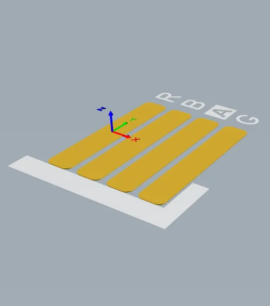
ジョイスティックコンポーネントのフットプリントの2Dおよび3Dビュー。3Dイメージは、コンポーネントのインポートされたSTEPモデルを示しています。パッドとコンポーネントのオーバーレイは、STEPモデルの下に表示されます。
このページに示されているフットプリントは、必要な手順を説明するためのものです。寸法が正確ではありません。新しいフットプリントの仕様は、常にメーカーのデータシートと照合してください。
コンポーネントフットプリントを手動で作成する一般的なシーケンスは次のとおりです:
-
設計空間の準備:スナップオプションの定義、グリッドとガイドの構成 - 詳細を学ぶ。
-
フットプリントは、PCB フットプリント エディターの中央にあるデザイン空間の参照点を中心に構築する必要があります。この参照点は、実際には設計空間の相対的な原点であり、配置操作と移動操作でカーソルによってコンポーネントフットプリントが選択される点です(PreferencesダイアログのPCB Editor – Generalページの現在のObject Snap Optionsによって異なります)。J、Rショートカットキーを使用して、基準点に直接ジャンプします。フットプリントの作成を開始する前に参照ポイントに移動するのを忘れた場合は、Edit » Set Referenceサブメニューコマンドを使用してリファレンスパッドをフットプリントに持ち込むことができます:
-
Pin 1 - コンポーネントの参照ポイントをコンポーネントフットプリントのピン1に設定します。
-
Center - コンポーネントの参照点をコンポーネントのフットプリントの中心に設定します。
-
Location - コンポーネントの参照点をユーザー定義の位置に設定します。
選択したポイントは0,0に設定されます - それが新しい相対原点となり、すべてのプリミティブの位置はこのポイントを基準にして更新されます。
-
コンポーネントの要件に従ってパッドを配置します(Place » Pad)。Place Padコマンドを実行した後、最初のパッドを配置する前に、Tabキーを押してPropertiesパネルを開き、パッドのDesignator、Size and Shape、Layer、Hole Size (スルーホール パッドの場合) など、すべてのパッド プロパティを定義します。指定子は、後続のパッド配置で自動的にインクリメントされます。表面実装パッドの場合は、LayerをTop Layerに設定します。スルーホールパッドの場合は、レイヤーをMulti-Layerに設定します。
一部のフットプリントには、不規則な形状のパッドが必要です。これはカスタム形状のパッドオブジェクトを使用して行うことができます。詳細については、パッドスタックのカスタマイズページを参照してください。
-
新しいコンポーネントフットプリントを作成する際の最も重要な手順の一つは、コンポーネントをPCBにはんだ付けするために使用されるパッドを配置することです。これらは、物理デバイスのピンに対応するように正確な位置に配置する必要があります。
-
パッドを指定する際には、Altium Designerが回路図シンボル上のピン番号からマッピングする際に使用するプロパティであるため、注意を払うべきです。
-
パッドの正確な配置を確保するために、このタスク専用のグリッドを設定することを検討してください。Ctrl+Gショートカットキーを使用してCartesian Grid Editorダイアログを開き、 Qキーを使用してグリッドをインペリアルからメトリックに切り替えます。
-
マウスでパッドを移動する際に正確に配置するには、キーボードの矢印キーを使用して現在のグリッド増分でカーソルを移動します。さらに、Shiftを押し続けると、グリッドの10倍のステップで移動します。現在のX、Yの位置はステータスバーに表示され、ヘッズアップディスプレイにも表示されます。ヘッズアップディスプレイには、位置と最後のクリック位置から現在のカーソル位置までのデルタが含まれます。Shift+Hショートカットを使用してヘッズアップディスプレイの表示を切り替えます。または、配置されたパッドをダブルクリックして必要なXおよびYの位置をプロパティパネルに入力します。
-
設計空間内の2点間の距離を確認するには、レポート » 距離測定(ショートカット Ctrl+M)を使用します。ステータスバーのプロンプトに従ってください。
-
パッド固有の属性、例えばはんだマスクやペーストマスクは、パッドの寸法と適用可能なマスク設計ルールに基づいて自動的に計算されます。マスク設定は各パッドに対して手動で定義することができますが、ボード設計プロセス中にこれらの設定を変更することは困難になります。通常、設計ルールでパッドを対象とすることが不可能な場合にのみこれが行われます。ルールはPCBエディタでボード設計中に定義されます。
-
トラック、円弧、その他のプリミティブオブジェクトを使用して、トップオーバーレイレイヤーのPCBシルクスクリーンに表示されるコンポーネントのアウトラインを定義します。配置中にコンポーネントをボードの下部に反転させると、オーバーレイは自動的にボトムオーバーレイレイヤーに転送されます。
-
トラックやその他のプリミティブ オブジェクトをメカニカル レイヤーに配置して、配置中庭などの追加のメカニカル詳細を定義します。メカニカルレイヤーは汎用レイヤーです。これらのレイヤーの機能を割り当て、フットプリント全体で一貫して使用する必要があります。
-
3D Bodyオブジェクトを配置して、PCBに実装する物理コンポーネントの3次元形状を定義します。
フットプリントに追加された3Dボディオブジェクトは、接続されたワークスペースにアップロードされた
3Dモデルを参照することができます。
-
指定子とコメント文字列は、PCB設計スペースに配置される際に自動的にフットプリントのオーバーレイレイヤーに追加されます。追加の指定子とコメント文字列は、メカニカルレイヤー上に.Designatorおよび.Comment特別な文字列を配置することで含めることができます。
指定子とコメント文字列を配置する際には、PCBエディタでレイヤーペアを定義する必要があります。これにより、文字列がコンポーネントが取り付けられた基板の側面に結びつけられ、コンポーネントが反転したときに基板の反対側にフリップする必要があります。詳細については、以下の
特定のレイヤー固有の要件の取り扱いセクションを参照してください。
-
フットプリントのプロパティ(例えば、その名前や説明)を、デザインスペースでオブジェクトが選択されていないときにアクティブになるLibrary OptionsモードのPropertiesパネルのFootprintタブで定義します(メインメニューからTools » Footprint Propertiesコマンドを使用してアクセスできます)。パネルのFootprintタブで利用可能なオプションとコントロールについて詳しくは、以下のセクションを参照してください。
-
すべてのフットプリントで標準化されたパッド/ビアの定義には、パッド/ビア配置に*.PvLibパッド/ビアライブラリを使用できます – 詳しくはこちら。
-
PCBフットプリントエディタは、フットプリント作成プロセスを迅速化するためのいくつかのウィザードも提供しています:
-
IPC Compliant Footprint Wizard – IPC標準7351の改訂Bに完全に準拠したPCBフットプリントを生成します – 表面実装設計およびランドパターン標準の一般要件 – 詳しくはこちら。
-
IPC Compliant Footprints Batch Generator – ファイルベースのPCBフットプリントライブラリを使用する場合、IPC Compliant Footprints Batch Generatorを使用して、複数の密度レベルで複数のフットプリントを迅速に生成します – 詳しくはこちら。
-
フットプリントウィザード – さまざまなパッケージタイプを選択し、適切な情報を入力すると、それに応じてコンポーネントフットプリントを構築します – 詳しくはこちら。
設計スペースの準備
デフォルトでは、グリッドはドットを使用して表示されます。好みに応じて、グリッドを線で表示することもできます。これは、下の画像に示されているように、Grid Editorダイアログで設定され、Propertiesボタンをクリックするか、Ctrl+Gショートカットを押してダイアログを開きます。

画像では、細かいグリッドがドットで表示され、粗いグリッドが線で表示されています。
プロパティパネル
PCBフットプリントエディタでフットプリントを編集しているとき、または現在デザインスペースで選択されている設計オブジェクトがないとき、プロパティパネルはLibrary Optionsを提示します。
パネルのGeneralタブの下で利用可能なオプションとコントロールについての情報を含む以下の折りたたみ可能なセクション:
選択フィルタ
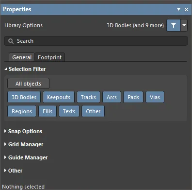
このパネルのセクションのオプションは、デザインスペースで選択できるPCBフットプリントオブジェクトを決定します。
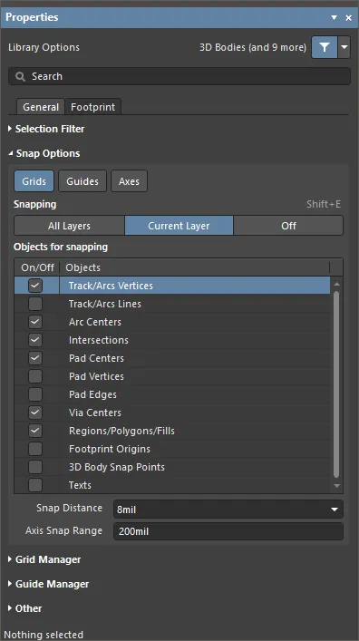
スナップオプション
-
Grids - カーソルがアクティブな設計空間グリッドにスナップするかどうかを切り替えるために使用します。このオプションが有効になっていると、カーソルは最も近いスナップグリッドの位置に引き寄せられます。アクティブなスナップグリッドはステータスバーとPCBエディタのヘッズアップディスプレイに表示されます(Shift+H ショートカットでオン/オフを切り替え)。
-
Guides - カーソルが手動で配置された線形またはポイントのスナップガイドにスナップするかどうかを切り替えるために使用します。スナップガイドはスナップグリッドを上書きします。
-
Axes - カーソルがスナップ対象のオブジェクトに対して軸方向(X方向またはY方向のいずれか)に整列するかどうかを切り替えるために使用します。Axis Snap Rangeは、XまたはY軸方向の整列が発生する距離を定義します。現在のカーソル位置から軸方向に整列したオブジェクトのスナップポイント(ホットスポット)まで、動的な整列ガイドラインが表示されます。
-
Snapping - 直接選択するか、Shift+E ショートカットを使用して、以下のオブジェクトにスナップするかどうかを選択します:
-
All Layers - このオプションを有効にすると、カーソルが可視レイヤー上の任意の電気オブジェクトにスナップします。
-
Current Layer - このオプションを有効にすると、カーソルが現在選択されているレイヤー上に配置されたオブジェクトのみを認識してスナップします。
-
Off - ホットスポットへのスナッピングをオフにするためにこのオプションを有効にします。
-
Objects for snapping
-
Snap Distance - カーソルが有効なオブジェクトのスナップポイントからこの距離以内にあり、アクティブレイヤーでスナッピングが有効になっている場合、カーソルはそのポイントにスナップします。
-
Axis Snap Range - カーソルが軸方向に整列し、Axesボタンが有効になっている場合、有効なオブジェクトのスナップポイントからこの距離以内にあると、整列が達成されたことを示す動的ガイドラインが表示されます。
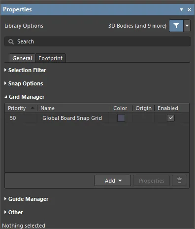
グリッドマネージャー
-
Grid Manager - ローカルでカスタマイズされたグリッドを定義および管理し、ボードのデフォルトスナップグリッドを設定する場所。
-
Priority - 設計空間では、描画順によって優先度が区別されます。最高優先度のグリッド(優先度1)が他のすべてのグリッドの前に描画され、次に優先度レベル2のグリッドが描画されます。これはデフォルトのGlobal Board Snap Gridに至るまで、他のすべてのカスタムグリッドの後ろに描画されます。
-
Name - グリッドの名前を表示します。
-
Color - 関連するグリッドの色を設定/変更するためのドロップダウンを開くためにクリックします。
-
Enabled - 関連するグリッドを有効にするためにチェックします。
-
Add
-
Properties - 選択されたグリッドのプロパティを変更するために、それぞれのグリッドエディタダイアログ(Cartesian Grid EditorまたはPolar Grid Editor)を開くためにクリックします。
-

 - 現在選択されているグリッドを削除するためにクリックします。
ガイドマネージャー
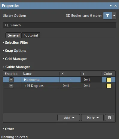
-
Guide Manager - ボードのための手動スナップガイドとスナップポイントの範囲を定義し、管理できる場所です。
-
Enabled - ガイドが設計スペース内で可視か(チェックあり)または非表示か(チェックなし)を示します。
-
Name - ガイドの名前です。
-
X - ガイドが通過するか、またはポイントが配置される設計スペース内のx座標(該当する場合)。
-
Y - ガイドが通過するか、またはポイントが配置される設計スペース内のy座標(該当する場合)。
座標は、関連するフィールドをクリックして値を入力することで定義できます。また、該当する場合/利用可能な場合は、フィールドの右側の

をクリックし、PCBフットプリント設計スペース内で直接必要なポイントを指定します。
-
Color - ドロップダウンを開いて関連するガイドの色を設定/変更するためにクリックします。
-
Add - 新しいスナップガイドまたはスナップポイントを追加するためにクリックします。必要なガイドタイプに対応するコマンドを関連するメニューから選択すると、新しいガイド/ポイントのエントリがグリッドに追加されます。以下のガイドタイプが利用可能です:
-
Add Horizontal Guide - このコマンドを使用して、設計スペース内の所望のY座標位置に水平ガイドラインを追加します。
-
Add Vertical Guide - このコマンドを使用して、設計スペース内の所望のX座標位置に垂直ガイドラインを追加します。
-
Add +45 Guide - このコマンドを使用して、所望のX,Y座標位置を通過する45度(y=x)のガイドラインを追加します。
-
Add -45 Guide - このコマンドを使用して、所望のX,Y座標位置を通過する-45度(y=-x)のガイドラインを追加します。
-
Add Snap Point - このコマンドを使用して、ポイントスナップガイドを追加します。これは、デフォルトのスナップグリッドの範囲内で手動でマークするホットスポットです。オブジェクトの配置や移動などのインタラクティブなプロセス中に、そのオブジェクトのホットスポットがそれに近接したときにポイントスナップガイドに「スナップ」します。
-
Place - ガイドを配置するためにクリックします。ドロップダウンからガイドタイプを選択します:
-
Place Horizontal Guide - このコマンドを使用して、設計スペース内の所望のY座標位置に水平ガイドラインを配置します。
-
Place Vertical Guide - このコマンドを使用して、設計スペース内の所望のX座標位置に垂直ガイドラインを配置します。
-
Place +45 Guide - このコマンドを使用して、所望のX,Y座標位置を通過する45度(y=x)のガイドラインを配置します。
-
Place -45 Guide - このコマンドを使用して、所望のX,Y座標位置を通過する-45度(y=-x)のガイドラインを配置します。
-
Place Snap Point - このコマンドを使用して、ポイントスナップガイドを配置します。これは、デフォルトのスナップグリッドの範囲内で手動でマークするホットスポットです。オブジェクトの配置や移動などのインタラクティブなプロセス中に、そのオブジェクトのホットスポットがそれに近接したときにポイントスナップガイドに「スナップ」します。
-
- 現在選択されているガイドを削除するためにクリックします。
その他
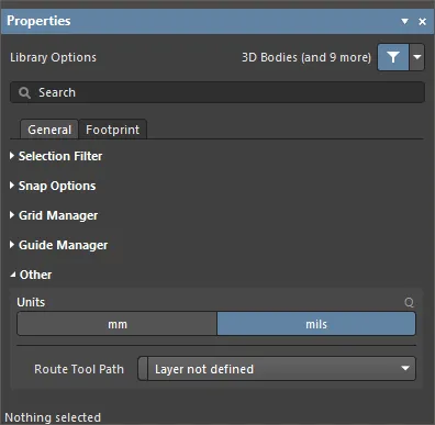
-
Units - 現在のPCBフットプリントドキュメントのデフォルト測定単位を選択するために使用します。デフォルト単位は、画面上またはレポート内の任意の距離関連情報を表示するために使用されます。距離関連情報を指定する際に単位の接尾辞(mmまたはmil)が入力されていない場合は、常にデフォルト単位が使用されます。
-
Route Tool Path - ボードのためのルートツールパスを定義するために使用される機械層(現在設計で使用可能になっているすべての層から選択)を選択するためのドロップダウンを使用します。
以下の折りたたみ可能なセクションには、パネルのFootprintタブの下で利用可能なオプションとコントロールに関する情報が含まれています:
Propertiesパネルの Footprintタブを使用してフットプリントのプロパティを定義する機能はオープンベータであり、PCB.FootprintParametersオプションは、Advanced Settingsダイアログで有効になっています。このオプションを無効にすると、フットプリントのプロパティは、メインメニューからTools » Footprint Propertiesコマンドを選択するか、PCB Libraryパネルのフットプリント領域でフットプリントエントリを選択して編集ボタンをクリックするか、PCB LibraryパネルのFootprints領域でフットプリントエントリをダブルクリックしてアクセスするPCB Library Footprintダイアログ ( )を使用して定義します。
設計オブジェクトが選択されると、そのオブジェクトタイプに特有のオプションがパネルに表示されます。以下の表は、PCBフットプリント設計スペース内で配置可能なオブジェクトタイプをリストしており、そのオブジェクトのプロパティページにアクセスするためのリンクをクリックします。
はんだおよびペーストマスクの拡張
はんだおよび/またはペーストマスクがPCBフットプリントエディタで正しく定義されているかを各パッドの端に現れるリングは、マルチレイヤーがレイヤー描画順序の最上位にあるため、トップソルダーマスク層の色で表され、マルチレイヤーパッドの下から拡張量だけ突出したソルダーマスク形状の端を表しています。これは上に描かれます。Layer Drawing Orderは、PreferencesダイアログのPCB Editor - Displayページで設定されます。
下の画像は、各パッドの端に現れる紫色(トップソルダーマスク層の色)の境界線があるPCBフットプリントを示しています。

レイヤーを素早く確認するには、シングルレイヤーモード(Shift+S)をCtrl+Shift+ホイールロールと組み合わせて使用します。
デフォルトでは、マスクレイヤー上に作成される形状は、フットプリントが配置されるPCBのSolder Mask ExpansionおよびPaste Mask Expansion設計ルールによって指定された量で拡大または縮小されたパッド形状です。場合によっては、拡張設計ルールをオーバーライドしてマスク拡張をパッド属性として指定したり、標準の定義済みマスク形状から選択したり、独自のカスタム形状を作成する必要があります。これらの状況では、選択したパッドのプロパティパネルでペースト/ソルダーマスクを設定できます - 詳細を見る。または、必要なマスクレイヤーに適切なプリミティブ(領域、トラックなど)を配置できます。
パラメータサポート
Altium Designerでオブジェクトに適用されるパラメータは、PCB設計に追加情報を加えるための強力で柔軟な手段を提供します。親オブジェクトのプロパティとして適用されるパラメータは、プロジェクト、ドキュメント、テンプレート、および設計ドキュメント内の個々のオブジェクトなど、さまざまなレベルで適用できます。
PCBスペースで利用可能になるパラメータは、クエリ、設計ルール、スクリプト、バリアントをフィルタリングするために使用でき、カスタム文字列を配置したフットプリントで呼び出すためにPCBコンポーネントフットプリントに適用できます。
エンジニアリング変更命令を通じたパラメータ
PCBパラメータ機能は、ECOメカニズムとPCBドキュメントに含まれる機能に基づいており、ユーザー定義のコンポーネントパラメータをPCBスペースに転送して保持することを可能にします。これは一方通行の転送であり、渡されたパラメータはPCBドメインで読み取り専用です。
パラメータ転送は、Design » Update PCB Documentメニューコマンドを使用して回路図からPCBにECOを作成することによって行われます。

ECOが実行されると(Execute Changesボタンを使用)、新しいユーザー定義の回路図コンポーネントパラメータがPCB設計の対応するフットプリント参照に転送されます。
パラメータの検出とPCBへの移行は、プロジェクトのオプション設定(Project » Project Options)によって決定されます。Project Optionsダイアログで、Differences Associated with Parametersセクションの差異検出と修正動作をComparatorタブおよびModifications Associated with ParametersセクションのECO Generationタブで設定します。
PCBエディタで転送されたパラメータを表示するには、コンポーネントをダブルクリックしてPropertiesパネルを開き、Parametersタブを選択します。このタブには、選択したコンポーネントフットプリントに割り当てられた現在のユーザーパラメータがリストされます。選択したコンポーネントフットプリントのパラメータも、Componentsパネルで利用可能です。
情報参照リンク
PCBドメインは、回路図から事前に定義されたComponentLinkパラメータを自動的に受け入れます。これらは通常、特定のファイルやインターネットの場所へのデータ参照リンクを確立するパラメータペア(説明とリンクURL)として定義されます。これは、通常、メーカーのウェブサイトやデータシートのURLです。
回路図とPCBデザインスペースの両方で、コンポーネントにカーソルを合わせると右クリックのコンテキストメニューからリンクにアクセスできます(Referencesサブメニューオプションの下)。特殊なパラメータはPropertiesパネルに追加され、PCBスペースに転送されると、コンポーネントフットプリントパラメータとして表示されます。

ソース フットプリントのパラメータ
PCBに渡されるパラメータは、コンポーネントのフットプリントを介して追加のボード製造または機能情報を提供するために使用できます。ソースライブラリレベルでフットプリントに特別なパラメータ文字列を追加することで、カスタム文字列はターゲットの機械層またはオーバーレイで解釈されます。
ユーザー定義パラメータを表す特別な文字列は、プロパティパネルの特別な文字列ボタンとドロップダウン( )を使用して、ソースコンポーネントのフットプリントに追加できます。

以下のライブラリフットプリントでは、特別な文字列.Designatorが機械2層に配置されています。

ユーザーパラメータを表す特別な文字列をコンポーネントフットプリントに追加できます。
そのカスタムパラメータが回路図のコンポーネントにも適用され、パラメータデータがPCBに転送された場合、解釈されたフットプリント文字列はボードビューと生成された出力ファイルの両方に表示されます。この場合、特別なパラメータ文字列には、組み立てを支援するカスタムコンポーネント部品識別子が含まれています。
ユーザーパラメータを特別な文字列としてコンポーネントフットプリントに適用することは、スイッチやコネクタの機能ラベルなど、他のカスタムPCB要件の範囲に役立ちます。ここでは、「機能」パラメータ文字列が、そのタイプのコンポーネントのフットプリントのトップオーバーレイに配置されるかもしれません。
ボードレイアウト上で特別な文字列の解釈された値を見るには、Special StringsオプションをView ConfigurationパネルのView OptionsタブのAdditional Options領域で有効にします。特別な文字列は常に生成された出力ファイルで変換されます。
回路図エディタで、必要に応じて、Display Names of Special Strings that have No Value DefinedオプションをPreferencesダイアログのSchematic – Graphical Editingページで有効にします。
パラメータクエリ
PCBドメインのパラメータ文字列は、Altium Designerクエリ言語を通じてアクセス可能であり、オブジェクトフィルタリング機能、特に類似オブジェクト検索機能で使用できます。
類似オブジェクトの選択を実行するには、コンポーネントを右クリックしてコンテキストメニューからFind Similar Objectsを選択し、Find Similar Objectsダイアログを開きます。

Find Similar Objectsダイアログには、必要に応じてフィルタリングオプションを選択できるParametersセクションが含まれています。

PCB Filterパネルは、フィルタ基準としてパラメータ固有のクエリワードを適用でき、PCBパラメータに基づいて設計ルールを作成するために使用できます。
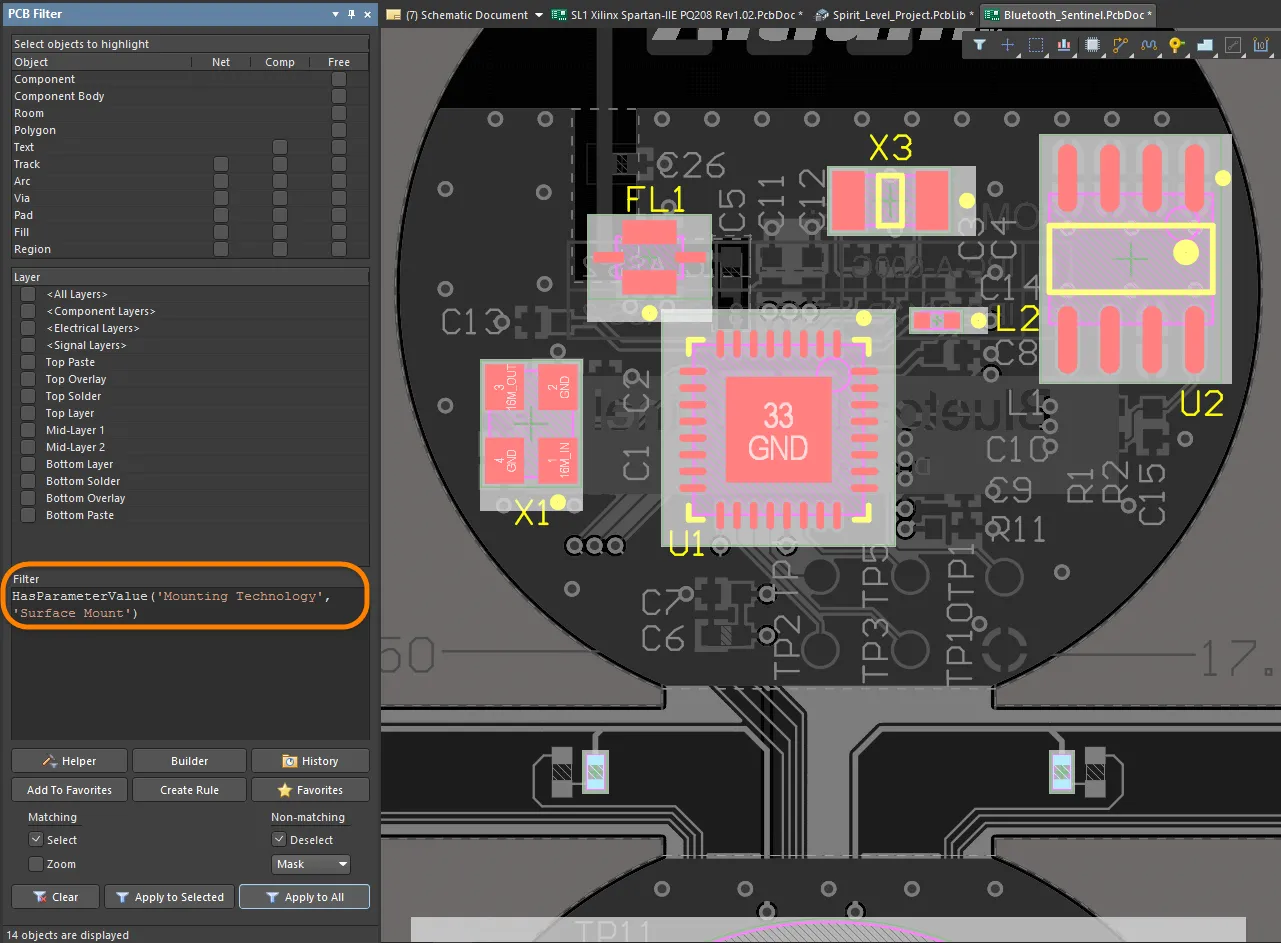
PCBフットプリントパラメータを扱うためのいくつかのクエリワードがあり、文字列値を数値に変換するための特定の機能ワード(StrToNumberなど)が含まれています。文字列値の変換は単位を認識しており(V、mA、mV、kOhmなど)、パラメータ値文字列の数値処理によってクエリ結果を決定できます。
クエリで指定できるサポートされている単位タイプは以下の通りです:
-
% – パーセント
-
A – 電流
-
C – 温度
-
dB – デシベル
-
F – 静電容量
-
G – 伝導率
-
H – インダクタンス
-
Hz – 周波数
-
Kg – 質量
-
m – 長さ
-
Ohm – 抵抗
-
Q – 電荷
-
s – 時間
-
V – 電圧
-
W – 力
-
Z – インピーダンス

PCBコンポーネントフットプリントパラメータを扱うためのいくつかのパラメータクエリワードがあります。
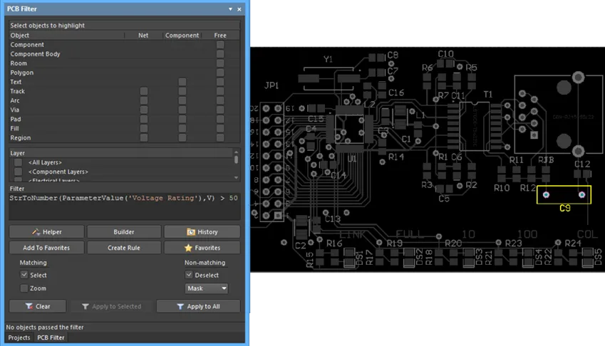
上記のクエリヘルパーダイアログに示されている例では、各コンポーネントの電圧定格パラメータを処理して(文字列から数値への変換を使用して - StrToNumber(単位値, 単位タイプ))、その値が50Vより大きいかどうかを判断します。PCBフィルタパネルで適用された場合、例のボードレイアウトは単一の高電圧コンポーネント、C1 (電圧定格値が3kVの)を露出させます。
科学的なE表記もサポートされているため、例えば、1nFを超えるキャパシタの値をフィルタリングするクエリは次のようになります:
StrToNumber(ParameterValue('CapacitanceValue'), F) > 1e-9
また、返されたParameterValueと比較値の両方に対して数値変換関数を使用することもできます:
StrToNumber(ParameterValue('CapacitanceValue'), F) > StrToNumber('1nF', F)
ルールとスクリプト
PCBパラメータクエリは、Altium Designerスクリプトやデザインルールにも適用できます。後者は、コンポーネントの配置やレイヤー割り当てを評価するために、フットプリントパラメータを検出するなどのレイアウト検証チェックを実行する場合があります。上記のQuery Helperダイアログにリストされている関数は、スクリプティング言語で利用可能です。
以下の例は、コンポーネント配置ルールに適用されたキャパシタの電圧定格クエリ(上記のフィルタクエリを参照)を示しており、実行時に高電圧(>50V)デバイスとして検出されたコンポーネントの特定のクリアランス値をチェックします。

特定のフットプリントパラメータによって定義されたデザインルールは、回路図空間から転送され、カスタムレイアウト条件を検出するために使用できます。
同様に、カスタムPCBパラメータは、例えば、コンポーネントがウェーブはんだ付けに対応しておらず、そのためにボトムレイヤーへの配置が必要な場合など、コンポーネントのレイヤー互換性をチェックするために使用できます。ここでは、カスタムの「WaveSoldering」パラメータ(Yes/No)を処理するオブジェクトマッチングクエリが許可されたレイヤールールに適用されるかもしれません。

(バッチ)ルールはその後、そのコンポーネントパラメータの値をチェックし、コンポーネントがボトムレイヤーへの配置と互換性がない場合に違反を作成します。
バリアント
PCBに転送されたパラメータは、デザインのバリエーション(デザインバリアント)に含まれ、バリアント選択で処理されます。
実際には、PCB空間の変化したコンポーネントパラメータは、クエリ文字列によって動的に検出されたり、特別な文字列を通じてボードレイヤーに表示されたりします。
ユーザー定義フットプリントパラメータ
Altium Designerでは、フットプリントのユーザー定義パラメータがサポートされています。PCBフットプリントエディタのデザインスペースにオブジェクトが選択されていない場合、Library OptionsモードのPropertiesパネルのFootprintタブのParameters領域で使用して、フットプリントパラメータを表示および編集できます。

PCBにコンポーネントが配置されると、これらのパラメータをのParametersタブのComponentモードのPropertiesパネルで確認できます。
-
PCB上に配置されたコンポーネントのフットプリントパラメータは、PCBエディタのメインメニューのMake PCB LibraryコマンドまたはMake Integrated Libraryコマンドによって生成されたライブラリに伝播されます。
-
フットプリントパラメータは、Altium Designerの比較エンジンによってサポートされ、生成されたピックアンドプレースおよびODB++出力にも使用されます。
Altium MCAD CoDesignerは、設定されたリンキングに従ってMCAD内のネイティブMCADコンポーネントを配置することをサポートします。場合によっては、複数のフットプリントが1つのコンポーネントにリンクされていることがあります(例えば、PCB上に2つの方法で取り付けることができるLED:垂直に、直線の脚で、または水平に、曲がった脚で)。フットプリントのパラメータを使用して、これらの異なるフットプリントから異なるMCADモデルを参照することができます。
ネイティブECADおよびMCADデザインコンポーネントのリンキングについてもっと学びましょう。
指定子とコメント文字列
デフォルトの指定子とコメント文字列
フットプリントがボード上に配置されると、デザインの回路図ビューから抽出された情報に基づいて指定子とコメントが与えられます。指定子とコメント文字列のプレースホルダーを手動で定義する必要はありません。なぜなら、フットプリントがボード上に配置されると自動的に追加されるからです。これらの文字列の位置は、デザインスペースで指定子またはコメント文字列が選択されたときのParameterモードのPropertiesパネルのAutopositionオプションによって決定されます。指定子とコメント文字列のデフォルトの位置とサイズは、PreferencesダイアログのPCB Editor - Defaultsページの該当するプリミティブで設定されます。

追加の指定子とコメント文字列
指定子またはコメント文字列の追加コピーが必要な場合があります。例えば、組み立て工場が各コンポーネントのアウトライン内に指定子を表示した詳細な組み立て図を求め、会社が最終PCB上のコンポーネントオーバーレイ上でコンポーネントのちょうど上に指定子を配置することを要求する場合です。この追加の指定子の要求は、フットプリントに.Designator特別な文字列を含めることで達成できます。.Comment特別な文字列も、コメント文字列の位置を代替レイヤーや位置に指定するために利用できます。
組み立て工場の要件に対応するために、.Designator文字列はPCBフットプリントエディタで機械レイヤーに配置され、このレイヤーを含むプリントアウトがデザイン組み立て指示の一部として生成されることになります。
特定のレイヤー固有の要件の処理
PCBコンポーネントには、接着ドットが必要であるか、または剥がせるはんだマスクの定義が必要であるなど、多くの特別な要件があります。これらの特別な要件の多くは、コンポーネントが取り付けられるボードの側面に関連しており、コンポーネントが反転されると他の側面に反転しなければなりません。
使用されることが少ない特別目的のレイヤーを大量に含めるのではなく、Altium DesignerのPCBエディタはレイヤーペアと呼ばれる機能を通じてこの要件をサポートしています。レイヤーペアは、ペアとして定義された2つの機械レイヤーです。コンポーネントがボードの一方の側から他方に反転されると、ペアの機械レイヤーの一方にある任意のオブジェクトがそのペアの他の機械レイヤーに反転されます。このアプローチを使用すると、接着ドット(または他の特別な要件)を含めるための適切な機械レイヤーを選択し、利用可能なオブジェクトを使用してその形状を定義します。ボード上にそのフットプリントを配置するときは、レイヤーペアリングを設定する必要があります。これにより、このコンポーネントがボードの他の側に反転されたときに、ソフトウェアがどのレイヤーにオブジェクトを転送する必要があるかを指示します。PCBフットプリントエディタでレイヤーペアを定義することはできません。これはPCBエディタで行われます。
コンポーネントが反転される前にレイヤーペアリングを定義する必要があります。ペアリングがコンポーネントがボトムサイドに移動した後に定義された場合、機械的な内容は反転しますが、元のレイヤーに留まります。反転する前にレイヤーペアを作成するのを忘れた場合は、ライブラリから更新して、ボード上に配置されたコンポーネントのインスタンスをリフレッシュできます。
機械レイヤーの名前は、View Configurationsパネルから直接編集でき、右クリックしてEdit Layerを選択します。
機械レイヤーの使用を管理する一般的なアプローチは、必要な機械レイヤー機能ごとに専用のレイヤー番号を割り当てることです。このアプローチは、すべてのデザイナーが同じレイヤー割り当ておよび番号付けスキームに従うことを要求します。また、同じ割り当ておよび番号付けスキームに従わない他のソースからコンポーネントを取得した場合には、デザインオブジェクトを現在の機械レイヤーからその機能に割り当てられた機械レイヤーに移動する必要があり、困難を生じることがあります。
この問題は、Layer Typeプロパティの導入によって解決されます。ライブラリからPCBエディタにコンポーネントが配置された場合、あるいはライブラリ間でコピーされた場合、またはIPC Footprint Wizardによって作成された場合、既存のレイヤータイプの割り当ては、それらのレイヤータイプに割り当てられた機械レイヤー番号に関係なく、自動的に一致します。オブジェクトは、そのレイヤータイプに従って正しいレイヤーに配置されます。ソフトウェアがレイヤータイプによる一致に失敗した場合、レイヤー番号による一致にフォールバックします。
個々の機械レイヤーとコンポーネントレイヤーペアの両方について、事前定義されたタイプのリストからレイヤータイプを選択できます。以下に示すダイアログにアクセスするには、個々のレイヤーを右クリックしてから、メニューからEdit LayerまたはAdd Component Layerコマンドを選択します。
コンポーネント関連の機械レイヤータイプに関する詳細情報については、
機械レイヤーの操作ページを参照してください。
PCBフットプリントに高さを追加する
最も単純なレベルの3D表現では、高さ情報をPCBフットプリントに追加できます。これを行うには、Properties パネルを Library Optionsモード (デザイン空間でオブジェクトが選択されていない場合にアクティブ) で開き、パネルのFootprintタブのHeightフィールドにコンポーネントの推奨高さを入力します。
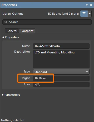
ボード設計中に高さの設計ルールを定義できます(PCBエディタでDesign » Rulesをクリック)、通常はコンポーネントクラス内またはルーム定義内の最大コンポーネント高さをテストします。
高さ情報を定義するためのより良いオプションは、PCBフットプリントに3Dボディを添付することです。
配線プリミティブを持つコンポーネントの管理
設計が転送されると、各コンポーネントで指定されたフットプリントが利用可能なライブラリから抽出されてボード上に配置されます。次に、フットプリント内の各パッドには、そのコンポーネントピンに接続されたネットの名前がネットプロパティとして設定されます。パッドに触れるすべてのオブジェクトは、パッドと同じネットに接続します。
PCBエディタには包括的なネット管理ツールが含まれています。これを起動するには、メインメニューからDesign » Netlist » Configure Physical Netsを選択してConfigure Physical Netsダイアログを開きます。オプションのメニューにはMenuボタンをクリックします。未割り当てのプリミティブに割り当てるネットを選択するためにNew Net Nameヘッダーのドロップダウンをクリックします。

同じピンに接続された複数のパッドを持つフットプリント
以下に示すフットプリントは、SOT223トランジスタで、複数のパッドが同じ論理的な回路図コンポーネントピン - ピン2に接続されています。この接続を行うために、同じ指定子 - '2'を持つ2つのパッドが追加されました。回路図エディタでDesign » Update PCBコマンドを使用して設計情報をPCBに転送すると、結果としての同期はPCBエディタで両方のパッドに接続線が表示されることを示します、つまり、それらは同じネット上にあります。これらの両方を配線できます。

SOT223フットプリントは、指定子が2の2つのパッドを示しています。
シルクスクリーンの準備
シルクスクリーンが露出した銅や穴と重なることによって発生する一般的な製造設計(DFM)問題を解決するために、PCBフットプリントエディタにはフットプリントのシルクスクリーンを準備するための専用機能が含まれています。これらの問題は、次のように効果的に対処できます:
-
シルクスクリーンの線とアークの自動クリッピング;
-
塗りつぶしと領域の自動クリッピングまたは移動;
-
シルクスクリーンテキスト文字列の自動移動。
シルクスクリーン準備ツールは、PCBを設計する際にもアクセスできます -
詳細を学ぶ。
PCBフットプリントエディタでシルクスクリーン準備ツールにアクセスするには、メインメニューからTools » Silkscreen Preparationコマンドを使用します。Silkscreen Preparationダイアログが開きます。

ダイアログを使用して、シルクスクリーンオブジェクトのクリッピング/移動の設定を構成します。利用可能なオプションは次のとおりです:
-
Clip to Exposed Copper – オブジェクトを自動的に露出した銅にクリップできるようにします。
-
Clip to Solder Mask Openings – オブジェクトをはんだマスク開口部に自動的にクリップできるようにします。
-
Silkscreen Clearance – シルクスクリーンオブジェクトと露出した銅/はんだマスクの開口部および穴との間の最小許容値を定義します。
-
Min Remaining Length – クリッピング後の線/円弧の長さが定義された値よりも小さい場合、そのオブジェクトはフットプリントから削除されます。この長さは頂点から頂点までの長さであり、エッジからエッジまでの長さではありません – ![]() 画像を表示。
画像を表示。
-
Move Text – シルクスクリーンのテキスト文字列と露出した銅/はんだマスクの開口部および穴との間の距離がSilkscreen Clearanceよりも小さい場合に、テキスト文字列を移動させることを有効にします。移動はMax Distanceの値によって制限されます。
-
Fill & Region – 塗りつぶしと領域と露出した銅/はんだマスクの開口部および穴との間の距離がSilkscreen Clearanceよりも小さい場合に実行されるアクションを選択します:
-
None – 塗りつぶしと領域はそのままにします。
-
Clip – Silkscreen Clearanceを維持するために、塗りつぶしと領域はクリップされます。適用可能な場合、塗りつぶしは領域に変換されます。
-
Move – 塗りつぶしと領域は露出した銅/はんだマスクの開口部および穴から離れるように移動されます。移動はMax Distanceの値によって制限されます。
-
Max Distance – テキスト文字列、コンポーネント指定子、塗りつぶし、領域がSilkscreen Clearanceを維持するために移動できる最大距離を定義します。
ダイアログの設定に従ってシルクスクリーンオブジェクトのクリッピングおよび/または移動を実行するには、OKをクリックします。
オブジェクトに対してアクションを実行できない場合(例えば、Max Distanceの制限のためにテキスト文字列を移動できない場合)、そのオブジェクトに関するメッセージがメッセージパネルに表示されます。
シルクスクリーン準備ツールのパフォーマンスの例を以下に示します。
IPC Compliant Footprint Wizardを使用したフットプリントの作成
IIPC Compliant Footprint Wizardは、IPC標準7351B版 - 表面実装設計およびランドパターン標準のための一般要件に完全に準拠したPCBフットプリントを生成します。このフットプリントウィザードとは異なり、IPC Compliant Footprint Wizardはコンポーネント自体からの寸法情報を使用し、その後、IPCによってリリースされたアルゴリズムに従って適切なパッドおよびその他のフットプリントプロパティを計算します。
フットプリントを定義するために使用されるパッドやトラックのプロパティを入力する必要がなく、ウィザードは実際のコンポーネント寸法を入力として受け取ります。IPC-7351標準のために開発された公式に基づき、ウィザードは、パッドやトラックなどの標準のAltium Designerオブジェクトを使用してフットプリントを生成します。
このダイアログは、IPC標準7351B版 - 表面実装設計およびランドパターン標準の一般要件に準拠しています。IPC-7351Bは2010年にリリースされ、2007年にリリースされたIPC-7351Aを置き換えました。

IPC Compliant Footprint Wizardを実行するには、メインメニューからTools » IPC Compliant Footprint Wizardを選択します。
Select Component Typeページで、フットプリントを作成したいコンポーネントのファミリーを選択します。Select Component Typeページ。ウィザードの右側にあるプレビューエリアは、現在選択されているコンポーネントを動的に表示し、生成が許可されているパッケージのタイプも示します。以下の表に、ウィザードでサポートされているコンポーネントタイプとパッケージを示します。
| 名前 |
説明 |
含まれるパッケージ |
| BGA |
ボールグリッドアレイ |
BGA, CGA |
| BQFP |
バンパー付きクアッドフラットパック |
BQFP |
| CAPAE |
電解アルミニウムコンデンサ |
CAPAE |
| CFP |
セラミックデュアルフラットパック - トリムおよび形成されたガルウィングリード |
CFP |
| チップアレイ |
チップアレイ |
チップアレイ |
| DFN |
デュアルフラットノーリード |
DFN |
| CHIP |
チップコンポーネント、2ピン |
コンデンサ、インダクタ、抵抗器 |
| CQFP |
セラミッククアッドフラットパック - トリムおよび形成されたガルウィングリード |
CQFP |
| DPAK |
トランジスタアウトライン |
DPAK |
| LCC |
リードレスチップキャリア |
LCC |
| LGA |
ランドグリッドアレイ |
LGA |
| MELF |
MELFコンポーネント、2ピン |
ダイオード、抵抗器 |
| MOLDED |
成形コンポーネント、2ピン |
コンデンサ、インダクタ、ダイオード |
| PLCC |
プラスチックリード付きチップキャリア、四角 - Jリード |
PLCC |
| PQFN |
プルバッククアッドフラットノーリード |
PQFN |
| PQFP |
プラスチッククアッドフラットパック |
PQFP, PQFP露出パッド |
| PSON |
プルバックスモールアウトラインノーリード |
PSON |
| QFN |
クアッドフラットノーリード |
QFN, LLP |
| QFN-2ROW |
クアッドフラットノーリード、2行、四角 |
ダブルロウQFN |
| SODFL |
スモールアウトラインダイオード、フラットリード |
SODFL |
| SOIC |
スモールアウトライン統合パッケージ、1.27mmピッチ - ガルウィングリード |
SOIC, SOIC露出パッド |
| SOJ |
スモールアウトラインパッケージ - Jリード |
SOJ |
| SON |
スモールアウトラインノンリード |
SON, SON露出パッド |
| SOP, TSOP |
スモールアウトラインパッケージ - ガルウィングリード |
SOP, TSOP, TSSOP |
| SOT143/343 |
スモールアウトライントランジスタ |
SOT143, SOT343 |
| SOT223 |
スモールアウトライントランジスタ |
SOT223 |
| SOT23 |
スモールアウトライントランジスタ |
3リード、5リード、6リード |
| SOT89 |
スモールアウトライントランジスタ |
SOT89 |
| SOTFL |
スモールアウトライントランジスタ、フラットリード |
3リード、5リード、6リード |
| WIRE WOUND |
精密ワイヤーワウンドインダクタ、2ピン |
インダクタ |
ウィザードの後続のページは、選択したコンポーネントタイプに応じて変わります。ウィザードの直感的なページに従って、必要な特定のコンポーネントフットプリントを設定してください。IPC Compliant Footprint Wizardを使用する際のいくつかの注意点:
-
すべての寸法は、ウィザードにメートル法(mm)単位で入力されます。
-
全体的なパッケージ寸法、ピン情報、ヒール間隔、はんだフィレット、および許容差を入力して、即座に表示することができます。
IPC許容差を変更すると、IPC準拠ではないPCBフットプリントが生成される可能性があります。
-
コートヤード、アセンブリ、コンポーネント(3D)ボディ情報などの機械的寸法を入力できます。
-
ウィザードは再入力可能で、レビューと調整が容易です。
-
フットプリントのプレビューは、各ステージで表示されます。各コンポーネントタイプについて、Previewエリアは、新しい位置、サイズなど、複数の設定に対して動的に更新されます。Previewエリアでは、 または
または をクリックして、2Dおよび3Dプレビュー画像を切り替えることができます。
-
必要に応じて、モデルを生成する前に 3D STEP モデルのプレビューを表示できます。コンポーネントタイプを選択した後、ウィザードの任意のページでGenerate STEP Model Previewをクリックすると、Preview領域に3D STEPモデルのプレビューが表示されます。
-
ペーストマスクは、大きなサーマルパッド(サイズ2.1mm x 1.6mm以上)を備えたパッケージ用に小さな充填物に分割されます。
-
ガルウィングリード線を含むパッケージの場合、パッドはトリミングされ、パッケージ本体の下に伸びるのを防ぎます。
-
中央の大きな熱パッドを持つ小型パッケージの場合、周辺のパッドはIPC標準に従ってパッド間に必要なクリアランスを確保するためにトリミングされます。
-
パッドのトリミングが適用されると、ダイアログ内に警告が表示されます。
-
フットプリントの名前と説明は、ウィザードで入力した情報に基づいて自動的に提案されますが、組織の要件に合わせて変更することができます。
-
IPC標準に従い、ウィザードは3つのフットプリントバリアント(_L、_N、_M)をサポートしており、それぞれが異なるボード密度に適したものです。
-
Finishボタンは、いつでも押して現在プレビューされているフットプリントを生成することができます。もしFinishをウィザードの全てを完了する前にクリックした場合、選択したコンポーネントタイプのシステムデフォルトを使用してフットプリントが作成されます。
-
ファイルベースのPCBフットプリントライブラリを使用している場合は、IPC準拠フットプリントバッチジェネレータを使用して、複数の密度レベルで複数のフットプリントを迅速に生成できます。
ウィザードがファイルベースのPCBフットプリントライブラリからアクセスされた場合、新しく作成されたフットプリントを保存する場所を選択できるFootprint Destinationページが利用可能です - ![]() 画像を表示:
画像を表示:
-
既存のPCBライブラリファイルにフットプリントを保存したい場合は、Existing PcbLib Fileを選択します。テキストボックスに直接ファイルを入力するか、を使用して希望のファイルを検索するダイアログを開くことができます。
-
新しいPCBライブラリファイルにフットプリントを保存したい場合は、New PcbLib Fileを選択します。テキストボックスに新しいPCBライブラリファイルの名前を入力します。システムは新しいライブラリファイル名に拡張子.PcbLibを追加します。
-
表示されているPCBライブラリファイルにフットプリントを保存するには、Current PcbLib Fileを選択します。
-
3D/STEPモデルを生成するには、Produce 3D/STEP modelを有効にします。
-
有効な「MCAD Co-Designer - SOLIDWORKS(R)」ライセンスを持っている場合、モデルをファイルタイプParasolidとして保存することを選択できます。Formatの右側のドロップダウンをクリックしてParasolidを選択します。External Fileテキストボックスに表示されるファイルは、*.x_tファイルです。これが保存されるファイルの名前と場所です。
-
Embedded(デフォルト)またはExternal Fileのいずれかを選択します。External Fileを選択して3D STEPモデルを外部ファイルとして保存します。デフォルトのファイルタイプはSTEPで、ファイル名はExternal Fileテキストボックスに*.stepのファイル拡張子とともに表示されます。必要に応じて、をクリックして生成された3D STEPモデルを保存するフォルダを選択します。
フットプリントウィザードを使用したフットプリントの作成
PCBフットプリントエディタにはFootprint Wizardが含まれています。このウィザードを使用すると、さまざまなパッケージタイプから選択し、適切な情報を入力すると、それに応じてコンポーネントフットプリントを構築できます。Footprint Wizardでは、パッドとコンポーネントオーバーレイに必要なサイズを入力します。

Footprint Wizardを起動するには、メインメニューからTools » Footprint Wizardを選択するか、設計スペースで右クリックしてコンテキストメニューからTools » Footprint Wizardコマンドを選択します。
Component patternsページを使用して、作成したいコンポーネントのパターンを指定します。リストから希望のパターンを選択し、ドロップダウンを使用してコンポーネントの単位(Imperial (mil)またはMetric (mm))を選択します。利用可能なパターンは:
-
ボールグリッドアレイ(BGA)
-
キャパシタ
-
ダイオード
-
デュアルインラインパッケージ(DIP)
-
エッジコネクタ
-
リードレスチップキャリア(LCC)
-
ピングリッドアレイ(PGA)
-
クアッドパック(QUAD)
-
抵抗器
-
スモールアウトラインパッケージ(SOP)
-
スタッガードボールグリッドアレイ(SBGA)
-
スタッガードピングリッドアレイ(SPGA)
ウィザードの後続ページは、選択したコンポーネントパターンに応じて変わります。ウィザードの直感的なページに従って、特定のコンポーネントフットプリントを必要に応じて設定してください。
エッジコネクタ、リードレスチップキャリア(LCC)、またはクアッドパック(QUAD)パターンのフットプリントのパッド命名スタイルを設定する際は、命名順序/方向を変更するために緑の矢印をクリックします – ![]() 画像を表示。
画像を表示。
コンポーネントレポートの生成
アクティブなPCBフットプリントのレポートを生成するには、メインメニューからReports » Componentコマンドを選択します。コマンドを起動すると、レポート(<PCBLibraryDocumentName>.CMP)がソースPCBライブラリドキュメントと同じフォルダに生成され、メインデザインウィンドウのアクティブドキュメントとして自動的に開かれます。レポートには、フットプリントの寸法や、フットプリントを構成するプリミティブオブジェクトの内訳、およびそれらが存在するレイヤーの情報が記載されています。
レポートは、ProjectsパネルのDocumentation\Text Documentsサブフォルダに自由文書として追加されます。

 AI-localized