PadとViaの概要

 パッドは、コンポーネントのピンに機械的な取り付けと電気的な接続の両方を提供するために使用されます
パッドは基本的な設計オブジェクトです。パッドは、コンポーネントをボードに固定し、コンポーネントのピンからボード上の配線への接続点を作成するために使用されます。パッドは単一の層に存在することができます。例えば、表面実装デバイスのパッドのように、またはZ平面(垂直)にバレル形状の本体を持ち、各(水平)銅層に平らな領域を持つ三次元のスルーホールパッドとして存在することができます。パッドのバレル形状の本体は、ボードが製造中にドリルされ、スループレートされるときに形成されます。XおよびY平面では、パッドは丸型、長方形、八角形、角丸長方形、面取り長方形、またはカスタム形状を持つことができます。パッドは、設計内の自由パッドとして個別に使用することも、より一般的には、PCBライブラリエディタで他のプリミティブと共にコンポーネントのフットプリントに組み込まれて使用されます。
から下層(青)へとスパンし、内部の電源層(緑)にも接続するビア。")
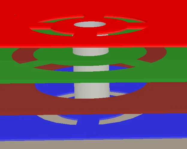
上層(赤)から下層(青)へとスパンし、内部の電源層(緑)にも接続するビア。
ビアは基本的な設計オブジェクトです。ビアは、PCBの2つ以上の電気層間の垂直電気接続を形成するために使用されます。ビアは三次元オブジェクトであり、Z平面(垂直)にバレル形状の本体を持ち、各(水平)銅層に平らなリングを持ちます。ビアのバレル形状の本体は、ボードが製造中にドリルされ、スループレートされるときに形成されます。ビアはXおよびY平面で丸型であり、丸いパッドのようです。ビアとパッドの主な違いは、ビアがボードのすべての層(上から下まで)をスパンするだけでなく、表面層から内部層へ、または2つの内部層間をスパンすることもできる点です。
ビアには以下のタイプがあります:
-
Thru-Hole – このタイプのビアは上層から下層へ通過し、すべての内部信号層への接続を可能にします。
-
Blind – このタイプのビアは、ボードの表面から内部信号層へ接続します。
-
Buried – このタイプのビアは、ある内部信号層から別の内部信号層へ接続します。
設計で使用できるビアのタイプは、レイヤースタックマネージャで定義されます。詳細については、ブラインド、埋め込み&マイクロビア定義ページを参照してください。
パッドとビアの直接配置
パッドとビアは、PCBおよびPCBフットプリントエディタの両方で配置が可能です。ビアは通常、インタラクティブまたは自動配線プロセス中に自動的に配置されますが、必要に応じて手動で配置することもできます。手動で配置されたビアは「フリー」ビアと呼ばれます。パッド(Place » Pad)またはビア(Place » Via)配置コマンドを起動すると、カーソルが十字線に変わり、配置モードに入ります。
-
カーソルを位置づけてクリックするかEnterを押してパッド/ビアを配置します。
-
さらにパッド/ビアを配置するか、右クリックまたはEscを押して配置モードを終了します。
パッド/ビアは、既にネットに接続されているオブジェクトの上に配置されると、ネット名を採用します。
配置中にAltキーを押すと、移動の方向が初期の移動方向に応じて水平または垂直軸に制約されます。
マルチレイヤー層のフリーパッドはビアに変更できます。フリーパッドとは、親コンポーネントオブジェクトの一部ではないパッドです。Gerberファイルを手動でPCB形式に戻すときに、フリーパッドをビアに変更することが役立ちます。設計スペース内で変換したいすべてのフリーパッドを選択し、メインメニューからTools » Convert » Convert Selected Free Pads to Viasコマンドを選択します。フリーパッドは同じ穴サイズのビアに変換されます。パッドの異なる層におけるサイズペアで見つかった最高値がビアの直径に使用されます。
また、ビアはフリーパッドに交換することができます。ビアをフリーパッドに変更すると、VIASが電源層とグランド層に接続するために使用されるPADS-PCBおよびPADS 2000ファイルをインポートする場合に便利です。これにより、編集可能なパッドを使用して、内部電源プレーンに適切に接続できます。デザイン空間で変換するすべてのビアを選択し、メインメニューからTools » Convert » Convert Selected Vias to Free Padsコマンドを選択します。ビアは、同じスタイル(Simple、Top-Middle-Bottom、またはFull Stack)で、同じ穴サイズのフリーパッドに変換されます。ビアの直径サイズは、該当するレイヤー上のパッドのXYサイズ設定に使用されます。パッドの形状はRound に設定されます。
グラフィカル編集
パッドとビアは、位置以外のグラフィカルなプロパティを変更することはできません。
-
フリーパッドを移動し、接続されているトラックも移動するには、パッドをクリックしたまま動かします。接続された配線は、パッドが移動してもパッドに接続されたままになります。パッドがコンポーネントに属している場合、パッドは移動しないことに注意してください。
-
PCBまたはPCBライブラリエディタで接続されたトラックを移動せずにフリーパッドを移動するには、Edit » Move » Moveコマンドを選択し、パッドをクリックしたまま移動します。
-
コンポーネントパッドの周りの選択四角形をクリックしてドラッグしても、実際にはコンポーネントの子オブジェクトであるため、選択されません。パッドのみをサブ選択するには、Ctrlキーを押しながら選択ウィンドウをクリックしてドラッグします。
-
ビアを配線とともに移動して配線またはコンポーネントスペースを増やす場合は、配線を移動するよりも再配線する方が効率的です。このソフトウェアには、Loop Removalと呼ばれる機能が含まれています。この機能を有効にすると、新しいパスに沿ってルートします(元のルートのどこかで開始および終了します)。右クリックしてインタラクティブ配線モードを終了するとすぐに、古い配線(ループ)は冗長なVIAも含めて削除されます。
Propertiesパネルによる非グラフィカル編集
この編集方法では、Propertiesパネルの関連モードを使用して、Pad/Via オブジェクトのプロパティを変更します。
ビアプロパティ

PropertiesパネルのViaモード
ネット情報
この領域では、ビアが属するネット、およびそのネットがメンバーである場合の差動ペアやxSignalに関する情報が提供されます。適切な場合はクラス情報が表示されます。Delay、Length、Max Current、およびResistanceの値も提供されます。
ネット情報について詳しくは、PCB配置と編集テクニックページを参照してください。
定義
-
Component – このフィールドは、選択されたビアがPCBコンポーネントの一部である場合にのみPCBエディタに表示され、親PCBコンポーネントの指定子が表示されます。クリック可能なComponentリンクを選択して、親コンポーネントのPropertiesパネルのComponentモードを開きます。
-
Net – ビアにネットを選択します。アクティブなボードデザインのすべてのネットがドロップダウンリストにリストされます。No Netを選択して、ビアがどのネットにも接続されていないことを指定します。デザインルールチェッカーがPCBオブジェクトが合法的に配置されているかどうかを判断するために、プリミティブのNetプロパティが使用されます。または、デザインスペース内のオブジェクトを選択してそのオブジェクトのネットを選択したビアに割り当てるために、Assign Netアイコン( )をクリックすることもできます。
-
Name – 一つ以上のビアが選択されている場合、ドロップダウンをクリックするとビアの名前が表示され、レイヤースタックで定義されているすべてのビアスパンがリストされます。ボード上で使用されるすべてのビアは、レイヤースタックで定義されているビアスパンのいずれかでなければなりません。
-
Propagational Delay – このフィールドには、信号の先頭が送信者から受信者に到達するまでの時間、つまり伝播遅延がリストされます。
-
Template – 現在のビアテンプレートを表示します。ドロップダウンから別のテンプレートを選択します。関連するLibraryがある場合、そのライブラリが表示されます。
ビアテンプレートリストは、PCBファイルが最初に開かれたときに作成され、現在の編集セッション中に配置されたビアがそのリストに追加されます。テンプレートビアのすべての配置されたインスタンスがボードから削除されると、そのビアはPCBファイルが保存され、閉じられ、再度開かれるまでテンプレートリストに残ります。
-
ライブラリ – 現在のライブラリに含まれる VIA テンプレートが表示されます。ビアをパッドビアライブラリ(*.PvLib) の場合、このフィールドにはそのライブラリの名前が含まれます。配置すると、 アイコンが有効になり、配置されたビアのプロパティがライブラリで定義され、編集できなくなったことを示します。
 アイコンが有効になっていない場合でも、コンテンツは編集できます。
-
(X/Y)
-
X (最初のフィールド) - このフィールドは、現在の原点に対するビアの中心の現在のX位置を示します。フィールドの値を編集して、現在の原点に対するビアの位置を変更します。値はメートル法またはインペリアル法で入力できます。単位が現在のデフォルトではない値を入力する場合は、単位を含めます。デフォルトの単位(メートル法またはインペリアル)は、Boardモード(デザインスペースでオブジェクトが選択されていない場合にアクセス)のPropertiesパネルのOther領域のUnits設定によって決定され、単位が指定されていない場合に使用されます。
-
Y (2番目のフィールド) - このフィールドは、現在の原点に対するビアの中心の現在のY位置を示します。フィールドの値を編集して、現在の原点に対するビアの位置を変更します。値はメートル法またはインペリアル法で入力できます。単位が現在のデフォルトではない値を入力する場合は、単位を含めます。デフォルトの単位(メートル法またはインペリアル)は、Boardモード(デザインスペースでオブジェクトが選択されていない場合にアクセス)のPropertiesパネルのOthe領域のUnits設定によって決定され、単位が指定されていない場合に使用されます。
この領域の右側にある アイコンは、XフィールドとYフィールドにアクセスするために
 (ロック解除)と表示されている必要があります。ロック/ロック解除アイコンを切り替えて、ロックステータスを変更します。
ビアスタック
-
Simple – 単純なビアを選択する場合に選択します。
-
Diameter – ビアの必要な直径を入力します。ビアの直径はすべてのレイヤーで同じです。
-
Relief – ビアのサーマル リリーフをカスタマイズし、適用可能なポリゴン コネクト スタイル ルールを上書きします。
-
Thermal Relief – Reliefオプションを有効にしたら、リンクをクリックしてPolygon Connect Styleダイアログを開き、必要に応じてサーマルリリーフオプションを変更できます。Edit Pointsボタンをクリックして、サーマルリリーフスパイクの接続ポイントを手動で定義します。
-
Top-Middle-Bottom – 選択して、最上層、すべての内部信号層、および最下層に異なる直径を選択します。
-
表示されているレイヤー – 表示されたレイヤーをクリックして、そのレイヤーのビアを設定します。選択したレイヤーがハイライト表示されます。
-
Diameter – ドロップダウンをクリックし、選択したレイヤーのビアの必要な直径を入力します。
-
Relief – ビアのサーマル リリーフをカスタマイズし、適用可能なポリゴン コネクト スタイル ルールを上書きします。
-
Thermal Relief – Reliefオプションを有効にしたら、リンクをクリックしてPolygon Connect Style ダイアログを開き、必要に応じてサーマルリリーフオプションを変更できます。Edit Pointsボタンをクリックして、サーマルリリーフスパイクの接続ポイントを手動で定義します。
-
Full Stack – オブジェクト経由のフルスタックを選択する場合に選択します
-
表示されているレイヤー – 表示されているレイヤーをクリックして、そのレイヤーのビアを設定します。選択されたレイヤーはハイライト表示されます。
-
Diameter – ドロップダウンをクリックしてから、選択されたレイヤーのビアの必要な直径を入力します。
-
Relief – ビアのサーマルリリーフをカスタマイズするために有効にします。これにより、適用可能なポリゴン接続スタイルルールが上書きされます。
-
Thermal Relief – Reliefオプションが有効になっている場合、リンクをクリックしてPolygon Connect Styleダイアログを開き、必要に応じてサーマルリリーフオプションを変更します。サーマルリリーフスパイクの接続ポイントを手動で定義するには、Edit Pointsボタンをクリックします。
-
Hole Size – このフィールドには、ビアの現在の穴サイズが表示されます。値は、製造中にビアに穿孔される穴の直径(円形、四角形、またはスロット形状)をミルまたはmmで指定します。穴サイズは0から1000ミルに設定でき、ビアよりも大きく設定して(銅なしの)機械的穴を定義することができます。このフィールドの値を編集してビア穴サイズを変更します。値はメートル法またはインペリアル法で入力できます。現在のデフォルトでない単位の値を入力する場合は、単位を含めてください。デフォルトの単位(メートル法またはインペリアル法)は、デザインスペースでオブジェクトが選択されていないときにアクセスされるBoardモードのPropertiesパネルのOther領域のUnits設定によって決定され、単位が指定されていない場合に使用されます。
-
Tolerance – 穴の公差属性を設定することで、ボードの適合と限界を決定するのに役立ちます。穴の最小(-)および最大(+)公差を指定します。Altium Designerにはデフォルトの穴公差値はありません。
コンポーネントのデータシートには、経年変化、摩耗、温度、めっき、材料、加工などの変動を考慮してプラス/マイナスの公差が記載されています。穴が穿孔されると、ドリルビットが摩耗して小さくなったり、ドリルが穴の中でわずかに振動したり揺れたりして、やや大きな穴ができることがあります。次に、取り付け穴がめっきされ、めっきはバッチごとやボード上の位置ごとに厚さが異なる場合があります。また、処理中にプリント回路基板PCBの基板が熱膨張または収縮することも考慮する必要があります。したがって、設計プロセスにおいて、すべての公差、ドリルの摩耗や揺れ、およびめっきの変動を考慮して穴の公差を設定することが重要です。
はんだマスク拡張
ビアタイプ&機能
-
IPC 4761 Via Type – ドロップダウンを使用して、IPC 4761規格のDesign Guide for Protection of Printed Board Via Structuresに従ってビアタイプを選択します。
-
グリッド – IPC 4761 Via TypeドロップダウンでNone以外のビア タイプが選択されている場合に表示されます。ボードのSideを選択し、選択したビアタイプに応じて使用可能な機能のMaterialを入力します。
プロパティでビア タイプが IPC-4761 に設定されているビアを PCB デザインに配置すると、新しいタイプのメカニカル レイヤーとコンポーネント レイヤーのペアがデザインに自動的に追加され、これらのレイヤーに対応する形状になります。
 IPC-4761 ビアタイプのメカニカルレイヤーは、自動的にデザインに追加されます。Top Tentingレイヤーは、例としてデザイン空間に示されています。
これらのレイヤーは、PCBプリントアウト、Gerber / Gerber X2、ODB ++、およびIPC-2581出力に使用できます。
Testpoint
Fabrication/Assembly – これらのオプションを使用すると、製造および/またはアセンブリテストでテストポイントの場所として使用するビアを指定できます。このビアをトップレイヤーのテストポイントとして定義するには、Topを有効にします。このビアを最下層のテストポイントとして定義するには、Bottomを有効にします。
パッドとビアのサーマルリリーフ
PropertiesパネルのPad Stack / Via Stack領域のThermal Reliefフィールドには、現在適用されているサーマルリリーフ設定がまとめられています。たとえば、Relief, 15mil, 10mil, 4, 90は、次のことを意味します:
-
サーマルリリーフ接続が適用されます。
-
エアギャップの幅は15milです。
-
サーマルリリーフ導体の幅は10milです。
-
サーマルリリーフ導体は90度回転します。
Thermal Reliefフィールドのチェックボックスが無効になっている場合、パッドとビアのポリゴンサーマルレリーフはルール駆動型、つまり、これらのレリーフは適用可能なポリゴン接続スタイルのデザインルールによって定義されます。個々のパッドの場合、必要なレイヤーに関連付けられたThermal Reliefオプションを有効にすることで、サーマルリリーフ構成をカスタマイズできます。この場合、サーマルリリーフはカスタムと見なされます。カスタムサーマルリリーフの定義「」の詳細をご覧ください。
はんだおよびペーストマスクの拡張
はんだマスクは、はんだマスク層の各パッド/ビアサイトで自動的に作成されます。はんだマスクはネガティブで定義されており、配置されたオブジェクトがはんだマスク層の開口部を定義します。ペーストマスクは、ペーストマスク層の各パッドサイトで自動的に作成されます。マスク層に作成される形状は、パッド/ビアの形状で、PCBエディタで設定されたはんだマスクの拡張およびペーストマスクの拡張の設計ルール、またはプロパティパネルで指定された量によって拡大または縮小されます。


はんだマスクが表示されたパッド。
パッドまたはビアを編集すると、Pad StackおよびSolder Mask Expansionの領域で、はんだマスクとペーストマスクの拡張設定がPropertiesパネルに表示されます。これらの設定は、パッド/ビアの拡張要件を局所的に制御するために含まれていますが、通常は必要ありません。一般的に、PCBエディタで適切な設計ルールを定義することによって、ペーストマスクとはんだマスクの要件を制御する方が簡単です。設計ルールを使用すると、ボード上のすべてのコンポーネントの拡張を設定するルールを設計し、必要に応じて、ボード上で使用される特定のフットプリントタイプのすべてのインスタンスや、特定のコンポーネントの特定のパッドなど、特定の状況を対象とする他のルールを追加できます。


設計ルールでマスクの拡張を設定するには:
-
Rule ExpansionオプションがPropertiesパネル(パッド用)のPad Stack領域のShapeとして選択されていること、および/またはRuleオプションがPropertiesパネル(ビア用)のSolder Mask Expansion領域で選択されていることを確認します。
-
PCBエディタでDesign » Rulesをメインメニューから選択し、Maskカテゴリの設計ルールをPCB Rules and Constraints Editorダイアログで確認します。これらのルールは、フットプリントがPCBに配置されるときに遵守されます。
拡張設計ルールをオーバーライドして、パッド/ビア属性としてマスクの拡張を指定するには、Manual ExpansionをPropertiesパネル(パッド用)のPad Stack領域のShapeとして、および/またはPropertiesパネル(ビア用)のSolder Mask Expansion領域のManualを選択し、必要な値を入力します。
スルーホールパッドのペーストマスク層は、DraftsmanドキュメントおよびGerber、Gerber X2、ODB++、IPC-2581、PCB Print出力でサポートされています。
パッドについては、標準の定義済みマスク形状から手動で選択するか、独自のカスタム形状を作成することもできます –
詳細を学ぶ。
パッドとビアのテンティング
パッドとビアの部分的および完全なテンティングは、適切な値をはんだマスクの拡張に定義することによって達成できます。この拡張制約は、Propertiesパネルでオブジェクトごとに定義するか、適切なはんだマスクの拡張設計ルールを定義することによって設定できます。拡張値を適切な値に設定することにより、以下を達成できます:
-
パッド/ビアを部分的にテントする – ランドエリアのみをカバーするには、マスクをパッド/ビアの穴まで閉じるように、拡張を負の値に設定します。
-
パッド/ビアを完全にテントする – ランドと穴をカバーするには、拡張をパッド/ビアの半径以上の負の値に設定します。
-
単一層のすべてのパッド/ビアをテントするには、適切な拡張値を設定し、はんだマスクの拡張ルールの範囲(フルクエリ)が必要な層のすべてのパッド/ビアを対象としていることを確認します。
-
さまざまなビアサイズが定義されているデザインですべてのパッド/ビアを完全にテントするには、拡張を最大パッド/ビア半径以上の負の値に設定します。個々のパッド/ビアをテントする場合、適用可能なデザインルールで定義された拡張に従うか、ルールをオーバーライドして指定した拡張を問題の個々のパッド/ビアに直接適用するオプションを使用できます。
テストポイント
関連ページ:ボード上のテストポイントの割り当て
このソフトウェアはテストポイントを完全にサポートしており、パッド(スルーホールまたはSMD)とビアを製造および/またはアセンブリテストのテストポイント位置として指定できます。パッド/ビアは、関連するテストポイントのプロパティを設定することで、テストポイントとして使用するように指定されます。これは、製造テストポイントまたはアセンブリテストポイントであるべきか、ボードのどちら側でテストポイントとして使用するべきかです。これらのプロパティは、PropertiesパネルのTestpoint領域にあります。
プロセスを合理化し、テストポイントのプロパティを手動で設定する必要性を軽減するために、ソフトウェアは、定義されたデザインルールに基づいて、テストポイントマネージャー(Tools » Testpoint Manager)を使用してテストポイントを自動的に割り当てる方法を提供します。いずれの場合も、この自動割り当てにより、パッド/ビアに関連するテストポイントのプロパティが設定されます。
パッド仕様
パッド指定子
各パッドには、最大 20 文字の英数字の指定子 (通常はコンポーネントのピン番号を表す) でラベルを付ける必要があります。パッド指定子は、最初のパッドに数字で終わる指定子がある場合、配置中に 1 ずつ自動的にインクリメントされます。最初のパッドの指定子は、配置する前にPropertiesパネルから変更します。
1A、1B、または1以外の数値増分などのアルファ増分を実現するには、Paste Specialダイアログ(Edit » Paste Special)のPaste Arrayボタンを押してアクセスするSetup Paste Arrayダイアログを使用します。

ペーストアレイ機能
パッドをクリップボードにコピーする前にパッドのデジグネータを設定すると、Setup Paste Arrayダイアログを使用して、パッドの配置時に指定シーケンスを自動的に適用できます。Setup Paste ArrayダイアログのText Incrementフィールドを使用すると、次のパッド指定子シーケンスを配置できます:
-
数字 (1, 3, 5)
-
アルファベット (A, B, C)
-
英数字の組み合わせ (A1 A2, 1A 1B, A1 B1, or 1A 2A, etc.)
-
数値でインクリメントするには、Text Incrementフィールドを、インクリメントする量に設定します。アルファベット順にインクリメントするにはText Incrementフィールドを、スキップする文字数を表すアルファベットの文字に設定します。たとえば、初期埋め込みの指定子が 1A の場合は、フィールドを A (アルファベットの最初の文字) に設定して、指定子を 1 ずつ増やします。フィールドを C (アルファベットの 3 番目の文字) に設定すると、指定子は 1A、1D (A の 3 文字後)、1G などになります。
ジャンパー接続
ジャンパ接続は、PCB上のプリミティブで物理的に配線されていないコンポーネントパッド間の電気的接続を定義します。これらは、ワイヤを使用して 1 つの物理層上のトラックを飛び越える 1 層ボードで特に便利です。
コンポーネント内のパッドには、Propertiesパネル内からJumper値でラベルを付けることができます。同じジャンパーと電気ネットを共有するパッドは、物理的に接続されていないが、それらの間に正当な接続があることをシステムに伝えます。
ジャンパ接続は、PCBエディタで曲線の接続線として表示されます。デザイン ルール チェッカーで、ジャンパ接続が未配線のネットとしてレポートされません。
ビア仕様
ビアプロパティの定義
各ビア タイプのレイヤ スパン(Z 平面)要件は、Layer Stack ManagerのVia Typesタブで定義されますが、ビアのサイズ プロパティは次のように定義されます。
配線ビアスタイル デザイン ルールの構成
メインページ:PCB設計ルールの定義、スコーピング、管理
インタラクティブ配線、ActiveRouting、または自動配線中に配置されたビアのサイズプロパティは、適用可能な配線ビアスタイルデザインルールによって制御されます。デザインルールでビアをターゲットにするために、ルールスコープで使用できる一連のビア関連のクエリキーワードがあります(Where the Object Matches)。これらについては、以下で詳しく説明します。
配線中にレイヤー変更を実行すると、ソフトウェアはこのレイヤー変更の開始レイヤーと停止レイヤーを確認し、レイヤースタックマネージャーから許可されたビアタイプを選択します。次に、最も優先度の高い適用可能な配線ビア スタイルデザイン ルールを特定し、そのルールのConstraintsセクションのビア サイズ設定を配置しようとしているビアに適用します。
例えば、DRAM_DATAネットのセットがあり、トップレイヤーからS2レイヤーへの遷移と、S2からS3レイヤーへの遷移にµViasが必要で、他のレイヤー遷移には全てドリルスルーホールビアが必要である場合(これは他のネットに必要なビアとも異なります)。これは、これらのDRAM_DATAネットを対象とする2つの配線ビアスタイル設計ルールを作成することで対応できます。適切なµVia設計ルールの例を以下に示します。画像にカーソルを合わせると、スルーホール設計ルールが表示されます。

設計ルールは、特定のタイプのビアに適用するようにスコープを設定できます。
ビアを自由空間に配置する場合、ソフトウェアは配置中に配線スタイル設計ルールを適用することができません。この状況では、デフォルトのビアが配置されます。
クエリキーワード
配線ビアスタイル設計ルールのスコープを簡素化するために、以下のビア関連クエリキーワードが利用可能です:
| ビアタイプクエリ |
返り値 |
| IsVia |
ビアタイプに関係なく、全てのビアオブジェクト。 |
| IsThruVia |
トップレイヤーからボトムレイヤーまでを貫通する全てのビア。 |
| IsBlindVia |
表面レイヤーから始まり内部レイヤーで終わるµViaでない全てのビア。 |
| IsBuriedVia |
内部レイヤーから始まり別の内部レイヤーで終わるµViaでない全てのビア。 |
| IsMicroVia |
µViaオプションが有効で、隣接するレイヤーを接続する全てのビア。 |
| IsSkipVia |
µViaオプションが有効で、2つのレイヤーを跨ぐ全てのビア。 |
利用可能なビア関連キーワードを見つけるために、クエリヘルパーのマスク機能を使用します。リストでクエリキーワードが選択されているときにF1キーを押すと、そのキーワードに関するヘルプが表示されます。

インタラクティブ配線中のビア配置
インタラクティブ配線中にレイヤーを変更すると、ソフトウェアは自動的にビアを挿入します。選択されるビアは、以下に依存します:
インタラクティブ配線中にレイヤーを変更するには:
-
数値キーパッドの*キーを押して、次の信号レイヤーに進みます。
-
Ctrl+Shift+WheelRollの組み合わせを使用して、レイヤーを上下に移動します。
L1からL4へのレイヤー変更中に配置されるスタックされたµVias。PropertiesパネルのInteractive Routingモードは、配置されるビアタイプを表示します。;6を押して、可能なビアスタックを順に切り替えます。;8を押すと、可能なビアスタックのリストが表示されます。
インタラクティブ配線中に配置されるビアの制御
-
レイヤー変更で跨がれるレイヤーの利用可能なビアタイプ。
-
そのレイヤー変更に選択されたビアタイプに対する適用可能な配線ビアスタイル設計ルール。
-
配線レイヤーを変更すると、ソフトウェアはそのレイヤースパンに最適なビアタイプを自動的に選択します。
-
使用できる複数のビアタイプ/組み合わせ(ビアスタック)がある場合 - 6ショートカットキーを押して、そのレイヤー変更に利用可能な全てのビアスタックを対話的に切り替えます。リストを表示するには、8ショートカットを押します。ビアスタックは、使用するµVia、Skip µVia、Blind via、Thruhole viaの順に提示されます。レイヤー変更が複数のレイヤーにわたる場合、適切なビアタイプが定義されていれば、スタックされたビアを配置できます。提案されたビアタイプは、ステータスバーとヘッズアップディスプレイに詳細が表示されます。例えば[µVia 1:2, µVia 2:3, µVia 3:4]のように、上の画像に示されています。
-
最後に使用したビアスタックは、次に配線するネットのデフォルトとして保持されます。デフォルトのビアスタックは、現在の編集セッションのみで保持されます。
-
ビア サイズ プロパティは、適用可能な配線ビアスタイルデザインルールによって指定され、適切なルーティング ビア スタイル デザイン ルールを定義するためのストラテジーについては、上記で説明します。
-
レイヤーの変更が実行されているときにビアのサイズをインタラクティブに変更するには、4ショートカットを押します。これにより、ビアサイズモードが循環します。Rule Minimum;Rule Preferred;Rule Maximum;User Choice現在のビアサイズモードがヘッドアップディスプレイとステータスバーに表示されます(上の画像を参照)。User Choiceを選択した場合は、Shift+Vを押してChoose Via Sizesダイアログを開き、希望するビアサイズを選択します。ダイアログに表示される使用可能なビア サイズのリストは、デザインで既に使用されているビアのリストから取得され、PCBパネルのPad and Via Templatesモードでこれらを検査します。
-
提案されたビア タイプの側面図は、上図のようにPropertiesパネルに表示されます。
-
ビアを配置して同じレイヤーに配線を続行するには、ショートカット2を押します。
-
この接続のビアを配置して配線を一時停止するには、テンキーの/ショートカットを押します。
-
配線するネットが内部電源プレーンに接続する場合は、テンキーの / キーを押して、適切な電源プレーンに接続するビアを配置します。これは、Any Angleモードを除くすべてのトラック配置モードで機能します。
-
Shift+F1を押すと、すべてのコマンド内ショートカットのメニューが表示されます。
スタックビアの操作
-
連続した接続を形成するスタックビアは、単一のビアであるかのように操作でき、スタックをクリックしてドラッグし、接続されたルーティングを使用してすべてを移動できます。
-
一度クリックすると、スタック内の最上位のビアが選択されます。マウスを動かさない場合、その後のシングルクリックで、スタック内の他のビアが順番に選択されます。
-
Ctrl+クリック&ドラッグで、選択したビアとそのルーティングのみを移動します。
-
スタック内のすべてのビアを選択するには、一度クリックして1つ選択し、Tabキーを押してそのスタック内のすべてのビアを含むように選択を拡張します。
ビアの表示の設定
ビアの操作に役立つ表示機能が多数あります。
ビア色
ビア色は、View Configurationパネルで設定します。ビアの銅線リングは、現在のMulti-Layer設定のLayersセクションに表示されます。ビアホールの色は、System ColorsセクションのVia Holes設定に表示されます。穴の表示を無効にするには、 を目的の設定に切り替えます。

スルーホールビアが最初の画像に示されています。2 番目の画像のビアはブラインド ビアです。穴は、開始レイヤーと終了レイヤーの色で表示されます。
ビアとはんだマスク
PCBエディタでのレイヤーのデフォルトの表示は、常にマルチレイヤーを最上位のレイヤーとして表示することです。これにより、特にパッドまたはビアが負のマスク拡張を使用している場合、はんだマスク層の内容が多層オブジェクトの下に消えるため、はんだマスク層の内容を正確に表示することが難しくなる可能性があります。これを変更するには、PreferencesダイアログのPCB Editor – Displayページでレイヤーの描画順序を変更します。描画する現在のレイヤーを最上位のレイヤーとして設定します。
レイヤーの描画順序を変更して現在のレイヤーを表示すると、トップソルダーを現在のレイヤーにすると、下の画像に示すようにマスクの開口部が正確に表示されます。緑色の矢印は、左がビアのソルダーマスク開口部のサイズ、中央がマスク開口部が収縮するパッド、右側が開口部が拡張されるパッドを示しています。
 はんだマスクの開口部を確認できるように、ディスプレイ設定を構成します。
スタックビアの表示
スタックされたビアがある場合、表示される番号は、スタック内のすべてのビアの開始レイヤーと終了レイヤーです。下の画像にカーソルを合わせると、ビアが3Dで表示され、画像の右側には3つのビアがスタックされています。
 スパンレイヤーはビアに表示できます。カーソルを合わせると、ビアが3Dで表示されます。
その他のビア表示設定
ビア スパンのビア ネット名とレイヤー番号を表示するには、View ConfigurationパネルのView OptionsタブにあるAdditional Options領域でVia NetsオプションとVia Spanオプションをそれぞれ有効にします。

パッドとビアホールのブラウジング
PCBパネルのHole Size Editorモードでは、その3つの主要な領域が上から順に以下を反映するように変更されます:
-
穴のタイプとそのステータスの一般的なフィルタリングと、ボードに現在定義されているレイヤードリルペアのサブセクション。
-
サイズと形状によって決定されるグループに配置されたUnique Holes。
-
穴オブジェクトの各グループを構成する個々のPads/Vias。

パネルセクションは、ホールタイプ、スタイル、およびステータスに適用された累積フィルタリングを表示します。
パネルのUnique Holes領域で、適切な列セルに値を入力することにより、ホールのグループを一括で編集できます。パッドとビアの現在のホールサイズを変更するために、Hole Size列に数値を入力できます。

6つの一致するホールスタイルの選択されたグループのホールサイズを編集します。
また、適用可能な場合、ホールのHole Length、Hole Type、およびPlatedのエントリも変更できます。

6つの一致するホールスタイルの選択されたグループのホールタイプを変更します。
選択されたホールグループに属する個々のパッド/ビアオブジェクトは、PCBパネルの下部Pad/Viaセクションにリストされています。リスト内のオブジェクトを右クリックしてPropertiesを選択するか(または直接エントリをダブルクリックして)、そのプリミティブの関連するPropertiesパネルのモードを開き、そのプロパティを表示および編集できます。
Hole Size EditorモードのPCBパネルをPCBの現在のドリルシンボルデータで更新するには、このモードでパネルの領域内を右クリックし、Refreshコマンドを選択します。
ドリルシンボルデータは、PCBドキュメントを保存するとき、およびこのデータを含むすべての出力に対して自動的に更新されます。
ドリルシンボルデータは、パフォーマンスを向上させるためにPCBパネルで自動的に更新されません。ドリルシンボルデータを手動で更新する機能は利用できます。PCB.LiveDrillSymbols オプションは、Advanced Settingsダイアログで無効になっています。
バックドリリングのサポート
PCBパネルのHole Size Editorモードは、バックドリルの対象となるパッドとビアの検査にも使用できます。バックドリルのレイヤーペアは、[BD]というテキストが追加されたLayer Pairsリストに表示されます。
バックドリル穴のサイズを選択すると、オブジェクトのKindがBackdrillとして表示されます。この機能を使用して、バックドリル穴をすばやく見つけて調べることができます。バックドリルの設定はパネルで編集できないことに注意してください。
バックドリルレポート
すべてのバックドリルイベントのレポートを生成するには、ユニークホールリストを右クリックし、コンテキストメニューからBackdrill Reportを選択します。
このレポートには、場所、掘削サイズ、掘削深さなど、各バック掘削イベントの詳細が表示されます。
カウンターホールのサポート
PCBパネルのHole Size Editorモードは、カウンターホール機能が有効になっているパッドを調査するためにも使用できます。PCB設計に一方または両方の側面にカウンターホール(カウンターボア/カウンターシンク)機能が有効になっているパッドオブジェクトがある場合、関連するCounterholes Topおよび/またはCounterholes BottomグループがLayer Pairsリストに表示されます。Counterhole DepthおよびCounterhole Angleの列は、パネルのUnique Holes領域に表示されることがあります。カウンターホール設定はパネルで編集できません。

設計内のカウンターホールに関する情報は、PCBパネルのHole Size Editorモードで表示されます。

 AI で翻訳