配線とは、各ネット内のノード間を接続する経路を定義するプロセスです。この経路は、ノード間に連続した接続を作成するために、トラック、アーク、ビアなどのPCB設計オブジェクトを銅層上に配置することで定義されます。これらのオブジェクトを1つずつ配置して接続経路を構築するのではなく、interactively route接続を行います。
PCBエディタにおいて、インタラクティブ配線はインテリジェントなプロセスです。コマンドを起動した後、パッドをクリックして配線する接続を選択します。インタラクティブ・ルータは、そのパッドから現在のカーソル位置までの配線経路を自動的に定義しようとします。
配置されるトラックの太さは、該当するRouting Width設計ルールによって制御され、他ネットのオブジェクトからのクリアランスは、該当する電気的Clearance設計ルールによって制御されます。インタラクティブ・ルータが、他ネットのパッドや配線など既存オブジェクトにどのように対応するかは、現在のRouting Conflict Resolutionモードに依存します。このモードによって、ルータが障害物をWalkaroundするのか、あるいはそれをPushしようとするのか、またはStopするのか、Ignoreするのかが決まります。
カーソル誘導配線により、障害物の周囲を回り込む複雑な手動配線を、素早く、簡単かつ直感的に行うことができます。言い換えると、マウスで配線経路を描くと、インタラクティブ・ルータがその経路に従ってトラックを配置しようとします。これは設計ルールに従って動作し、トラック配置やコーナー形状に関するさまざまな制約にも対応します。
インタラクティブ配線は、次の対象に対して実行できます:
-
単一ネット – Route » Interactive Routing
-
差動ペアとして構成された2つのネット – Route » Interactive Differential Pair Routing – 詳細
-
選択されたネットのセット – Route » Interactive Multi-Routing – 詳細
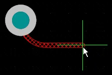
インタラクティブに接続を配線する – コマンドを起動して接続ラインをクリックすると、インタラクティブ・ルータはネットオブジェクトから現在のカーソル位置までの経路を、既存オブジェクトを避けながら探索します。マウスボタンをクリックすると、ハッチ表示されたすべてのトラックセグメントが配置され、Ctrl+Clickして配線を自動完了します。
Interactive Routing Tips
-
Route » Interactive Routingコマンド(アクティブバー上の ボタン、ショートカット:
 Ctrl+W)を実行し、ネット属性を持つオブジェクトをクリックして配線を開始します。これはパッド、接続ライン、既存のビア、部分的に配線されたネットのトラック終端など、そのネットに属する任意のオブジェクトでかまいません。
-
PCBエディタは、そのネット上で最も近い電気オブジェクト(パッド中心やトラックセグメント終端など)にジャンプし、そこから現在のカーソル位置までの配線経路を定義しようとします。
-
インタラクティブ配線を開始すると、PCBエディタはトラックオブジェクトの配置を開始できるだけでなく、次のことも行います:
-
カーソル位置とマウスクリックを監視し、適用可能なすべての設計ルールを適用します。
-
カーソルの軌跡に追従し、配線セクションを配置するために必要な操作回数を最小限に抑えます。
-
接続性を監視し、配線が完了するとすぐに接続ラインを更新します。
-
*キー(テンキー)を押して次のシグナル層へプッシュする、あるいは配線ビアスタイル設計ルールに従ってビアを挿入するなど、配線専用のショートカットをサポートします。
-
配線中は、カーソル位置までのトラックをクリックして配置し、その後カーソルを動かし続ける、という操作を繰り返します。これは、選択した経路をソフトウェアが正確に維持できるようにするためです。トラックを確定する前に遠くまで進みすぎると、経路の一部が変更される場合があります。
-
ショートカットよりパネル操作を好む場合は、Tabを押して配線を一時停止し、PropertiesパネルのInteractive Routingモードを開きます。
-
現在の配線モード、幅、ギャップ、ビアサイズなど多くの設定は、ステータスバーまたはヘッズアップディスプレイ(Shift+Hで表示/非表示を切り替え)に表示されます。
-
インタラクティブ・ルータが現在のカーソル位置に到達できるかどうかは、現在のRouting Conflict Resolutionモードに依存します。このモードは、Status bar( )およびインタラクティブ配線コマンド実行中のHeads Up Displayに表示されます。
-
Shift+Rを押して、利用可能なコンフリクト解決モードを順送りに切り替えます。どのモードを利用可能にするかは、Interactive Routingページ(Preferencesダイアログ内)で設定できます。
-
モードがWalkaround、 Push and Hug、またはPushに設定されている場合、インタラクティブ・ルータは、下のビデオに示すように、既存オブジェクトの周囲や間を通る経路を探索します。
-
可能性のある配線経路セグメントは、ハッチ表示(次のクリックで配置)または中抜き表示(先読みセグメント。これを見て前のセグメント終端位置を判断)で表示されます。
-
ClickまたはEnterを押して、ハッチ表示されたすべてのセグメントを配置します。
-
右クリックまたはEscで現在の配線を終了します。終了前に確定された配線は保持されます。
-
Spacebarを押してコーナー方向を切り替えます。
-
Shift+Spacebarを押して、利用可能なコーナーモードを順送りに切り替えます(詳細)。
-
Backspaceを押して、最後に配置したセグメントを「リップアップ」します。最後のセグメント配置時にpushedされていたオブジェクトがある場合、それらは元の位置に戻されます。この機能は自動完了を使用した後は利用できません。
-
配線層を切り替えてビアを挿入するには:
-
テンキーの*キーを押して、次に利用可能なシグナル層に切り替えるか、
-
テンキーの+キーと-キーを押すか、
-
Ctrl+Shift+Wheel Scrollショートカットの組み合わせを使用するか、
-
8キーを押して、利用可能なVia Typeから選択します(詳細)。
-
スルーホールパッドまたはビア上でクリックして配線を開始した際に、誤った層にいることに気付いた場合は、Lを押します。押すたびに、次に利用可能なシグナル層へと切り替わります。
-
テンキーの/を押してビアを挿入し、その接続を解放します(ファンアウトに使用)。
-
2を押してビアを挿入し、層を切り替えずに(同じ層で)配線を続行します。
-
Ctrl+Clickを押すと、インタラクティブ・ルータに現在の配線を自動完了させるよう指示します。自動完了されない場合でも、その接続が配線不可能という意味ではありません。距離が長すぎるか、終端点が別の層にある可能性があります。
-
Quick RoutingおよびQuick Differential Pair Routingコマンドは、設定や機能を絞り込んだ軽量な配線機能を提供し、より単純な設計に適しています。
-
このページでは、単一ネットをインタラクティブに配線する手順と、そのプロセスを制御する設定について説明します。差動ペア配線やインピーダンス制御配線など、特殊な配線手法に関する情報を探している場合は、Routing the PCBページのリンクを参照してください。
-
配線中にShift+F1を押すと、利用可能なインコマンドショートカットのメニューが表示されます。メニューからコマンドを選択するか、各コマンドの横に表示されているショートカットキーを使用できます。
インタラクティブ配線中の接続性の監視
PCBエディタにはネットアナライザが搭載されており、デザイン空間内のすべてのオブジェクトの位置を常に監視し、ネットタイプオブジェクトが編集されるたびに接続ラインを更新します。ネットアナライザは、そのネットに接続されているすべてのオブジェクトを監視します。たとえば、ある接続が配線されると、その2つのパッド間の接続ラインはネットアナライザによって自動的に削除されます。ネットが部分的に配線されている場合は、そのネット上で最も近い2つの配線ポイント間に、短くなった接続ラインが表示されます。
接続ラインを無視して、別の位置から/へネットを配線しても問題ありません。配線が終了するとすぐにネットアナライザが実行され、不要になった接続ラインは削除されます(下のビデオ参照)。

接続ラインはパッド中心同士を結んでいますが、実際の配線経路は自由に選択できます。ネットアナライザは配線の進行状況を常に監視し、接続ラインを更新します。
接続ラインの配置は配線トポロジ設計ルールによって決定されるため、接続ラインがトラック終端ではなく、ネット内の別の点(他の点により近い位置)に接続される場合があります。必要に応じて、Smart Track Endsオプションを有効にすることで、接続ラインをトラック終端に強制的に接続させることができます。このオプションは、PCB Editing – Generalページ(Preferencesダイアログ内)で設定します。下のビデオはその動作を示しています。なお、そのネットに属するオブジェクトに対して編集操作を行うことで、ネットアナライザを強制的に実行し、接続ラインを更新させることができます。編集操作には、オブジェクトの移動、オブジェクトのクリック&ホールド、オブジェクトのプロパティを表示するためのダブルクリックなどが含まれます。

GNDネットの接続ラインが、配線終端ではなくパッド1に接続されている点に注目してください。Smart Track Endsを有効にして何らかの編集を行うと、接続ラインは配線終端へとジャンプします。
PCBデザイン空間における接続性の詳細については、Understanding Connectivity on Your PCBページを参照してください。
デザイン空間における配線位置の決定方法
PCBエディタはグリッドベースの編集環境であり、デフォルトの動作として、インタラクティブ配線は現在のスナップグリッド上に配置されます。スナップグリッドに加えて、設計オブジェクトを正確に配置・整列させるための、さまざまなスナップ機能が用意されています。これらを総称してUnified Cursor-Snap Systemと呼びます。
このシステムの主な要素は次のとおりです:
-
User-Definable Grids – 直交(Cartesian)および極座標(Polar)形式の両方で利用可能なグリッド。
-
Object Snapping – 配置済みオブジェクトのスナップポイント(ホットスポット)へのカーソル近接に基づき、カーソル位置をそのオブジェクト側へ引き寄せる機能です。例えば、グリッド外のパッド中心へカーソルを引き寄せる場合に使用します。
-
Snap Guides – 自由に配置でき、オブジェクトの位置合わせに便利な視覚的ガイドを提供します。
-
Axis Snapping – 近くのオブジェクトのホットスポットと軸方向に整列するよう、カーソルを X または Y 方向のいずれかに引き寄せる機能です。
カーソルスナップ機能のデモンストレーション。
Snap System オプションは次の場所で設定します:
Working with the Cursor-Snap Systemについて詳しく学ぶ
インタラクティブ配線の基本
インタラクティブ配線コマンドを起動し、接続ラインをクリックすると、インタラクティブ配線エンジンは、パッドや既存のトラックなど最も近い既存ネットオブジェクトから現在のカーソル位置まで、利用可能な最短経路に沿って接続されたトラックセグメントのチェーンを追加します。
これらのトラックセグメントは、まだ配置されていない提案セグメントであることを示すためにハッチ表示されます(uncommitted)。左クリックしてそれらのセグメントを配置すると、実線になります。これらの実線セグメントは soft commits と呼ばれます。これは、ソフトウェアがそれらを保持したいセグメントとして認識していることを意味しますが、配線パスによって冗長になったり不正な形状を作成したりする場合、インタラクティブ配線エンジンはそれらを削除したり、再び uncommitted(ハッチ表示)に戻したりすることがあります。この動作は、このページ最初のビデオで示されています。
シンプルなボードをインタラクティブに配線する様子。
配線を開始するために接続ラインをクリックすると、ソフトウェアは最も近い既存ネットオブジェクトにジャンプします。選択されたネットオブジェクトを変更するには:
-
9 を押して、接続ラインの反対側のネットオブジェクトに切り替えます。切り替え先オブジェクトの位置が現在のウィンドウ内にない場合、ビューはジャンプして新しいカーソル位置を中心に表示されます。
-
2 本以上の接続ラインが接続されている場合、7 を押して別の接続ラインに切り替え、同じネットオブジェクトを維持します。
-
Shift+F1 を押して、コマンド中に使用できるショートカットの一覧を表示します。
インタラクティブルーターの設定
インタラクティブ配線のデフォルト設定は次の場所で行います:
以下の折りたたみセクションには、インタラクティブ配線のオプションとコントロールに関する情報が含まれています:
Net Information

-
Net Name – インタラクティブに配線しているネット名。
-
Net Class – 配線中のネットが属しているネットクラス(ネットクラスのメンバーである場合)。
-
Length – 合計 Signal Length。Signal Length はノード間の総距離を正確に算出した値です。配置済みオブジェクトを解析して、スタックまたは重なり合うオブジェクトやパッド内の蛇行パスを解決し、ビア長も含めます。
-
Delay – 未配線部分を含む、選択されたセグメントの総遅延。
Interactive Routing パネルの Properties モードから、Net Name、Net Class、Length、Delay のクリック可能なリンクを選択すると、PCB – Nets パネル に移動し、関連するネットの詳細を表示および変更できます。
Properties

-
Layer – ドロップダウンを使用して、配線を行うレイヤーを指定します。
-
Via – ビアがテンプレートに関連付けられている場合、そのテンプレート名がここに表示されます。
-
Via Diameter – ビア径を指定します。
-
Via Hole Size – ビアホールサイズを指定します。
-
Width – ドロップダウンを使用して幅を指定します。
-
Min – 現在のネットに定義されているデザインルールの最小幅を使用することを示します。
-
Preferred – 現在のネットに定義されているデザインルールの推奨幅を使用することを示します。
-
Max – 現在のネットに定義されているデザインルールの最大幅を使用することを示します。
Interactive Routing Options

-
Routing Mode – ドロップダウン、またはショートカット Shift+R を使用して、目的の配線モードを順に切り替えます。次の選択肢があります:
-
Ignore Obstacles – 既存オブジェクトを無視して(自由に配線可能)、違反箇所をハイライト表示します。
-
Walkaround Obstacles – Interactive Router が既存のトラック、パッド、ビアを回避して配線するように選択します。このモードで違反を発生させずに障害物を回避できない場合、ルートがブロックされていることを示すインジケータが表示されます。
-
Push Obstacles – Interactive Router が既存トラックを移動して新しい配線のためのスペースを確保するように選択します。このモードではビアを押してスペースを作ることもできます。このモードで違反を発生させずに障害物を押しのけることができない場合、ルートがブロックされていることを示すインジケータが表示されます。
-
HugNPush Obstacles – Interactive Router が既存のトラック、パッド、ビアに可能な限り密着して配線し、必要に応じて障害物を押して配線を継続するように選択します。このモードで違反を発生させずに障害物に密着または押しのけることができない場合、ルートがブロックされていることを示すインジケータが表示されます。
-
Stop At First Obstacle – このモードでは、配線エンジンは最初に遭遇した障害物で停止します。
-
AutoRoute Current Layer – 現在のレイヤーのみで自動配線を有効にします。
-
AutoRoute MultiLayer – 複数レイヤーで自動配線を有効にします。
-
Corner Style – 希望する配線コーナースタイルを選択するか、ショートカット Shift+Spacebar を使用してコーナースタイルを順に切り替えます。
-
Gloss Effort (Routed) – 希望するグロスレベルをパネルから直接選択するか、ショートカット Shift+Ctrl+G を使用して次の選択肢を順に切り替えます:
-
Off – このモードでは、グロッシングは事実上無効です。ただし、配線/ドラッグ後には、重なり合うトラックセグメントを除去するなどのクリーンアップは引き続き実行されます。このモードは通常、トラックの手動ドラッグやパッドエントリのクリーンアップなど、ボードレイアウトの最終段階で細かな調整を行う際に有用です。
-
Weak – このモードでは、Interactive Router が現在配線中のトラック(またはドラッグ中のトラック/ビア)に直接接続されている、またはその周辺にあるトラックのみを考慮して、低レベルのグロッシングを適用します。このグロッシングモードは、トラックレイアウトの微調整やクリティカルな配線を扱う場合に有用です。
-
Strong – このモードでは、Interactive Router が最短経路を探し、トラックをスムージングするなど、高レベルのグロッシングを適用します。このグロッシングモードは、ボードの多くを素早く配線することを目的としたレイアウト初期段階で有用です。
-
Gloss Effort (Neighbor) – 現在配線中のネットによって押されるトレースに適用するグロスレベルを、次の選択肢からパネルで直接選択します:
-
Off – このモードでは、グロッシングは事実上無効です。ただし、配線/ドラッグ後には、重なり合うトラックセグメントを除去するなどのクリーンアップは引き続き実行されます。このモードは通常、トラックの手動ドラッグやパッドエントリのクリーンアップなど、ボードレイアウトの最終段階で細かな調整を行う際に有用です。
-
Weak – このモードでは、Interactive Router が現在配線中のトラック(またはドラッグ中のトラック/ビア)に直接接続されている、またはその周辺にあるトラックのみを考慮して、低レベルのグロッシングを適用します。このグロッシングモードは、トラックレイアウトの微調整やクリティカルな配線を扱う場合に有用です。
-
Strong – このモードでは、Interactive Router が最短経路を探し、トラックをスムージングするなど、高レベルのグロッシングを適用します。このグロッシングモードは、ボードの多くを素早く配線することを目的としたレイアウト初期段階で有用です。
-
Automatically Terminate Routing – 有効にすると、ターゲットパッドまでの配線を完了した際、配線ツールはターゲットパッド from からそのまま配線モードを継続するのではなく、リセットされ、次に配線を開始するソースパッドをクリックできる状態になります。このオプションを無効にすると、ターゲットパッドまで配線した後もツールは配線モードのままで、前のターゲットパッドを次の配線のソースとして使用します。
-
Automatically Remove Loops – 手動配線中に作成された冗長ループを自動的に削除するには有効にします。これにより、冗長トラックを手動で削除することなく接続を再配線できます。ただし、電源ネットなどループが必要なネットを配線する場合もあります。そのような場合には、ショートカット Shift+D を使用して、同じネットに対するこのグローバル設定を一時的に上書きできます。
-
Remove Loops With Vias – ビアを含むループを自動的に削除するには有効にします。ループ削除時にビアを残したい場合は、このオプションを無効にします。
-
Remove Net Antennas – 他のプリミティブに接続されておらずアンテナ形状となっているトラックまたはアークの端部を削除するには、このオプションを有効にします。
-
Allow Via Pushing – Push Obstacles または HugNPush Obstacles モードでビアを押せるようにするには、このオプションを有効にします。
-
Pin Swapping – ピンのスワップを有効にするにはこのオプションをオンにするか、ショートカット Shift+C を使用します。
-
Auto Shrinking – 現在選択されている配線幅では障害物間を通せない箇所で、配線が可能となる値まで配線幅を自動的に縮小するには、このオプションをオンにします。Routing Auto-shrinking について詳しく学んでください。
-
Display Clearance Boundaries – 有効にすると、既存オブジェクトと適用されるクリアランスルールによって定義される進入禁止クリアランス領域が、ローカルビューサークル内にシェーディングされたポリゴンとして表示されます。また、配線中にショートカット Ctrl+W を使用してオン/オフを切り替えることもできます。このオプションは Ignore Obstacles 配線モードでは使用できません。
-
Reduce Clearance Display Area – より小さなクリアランス境界を使用できるようにします。このオプションは、Display Clearance Boundaries option が有効な場合にのみ使用できます。
-
Show Length Gauge – 現在の配線長を表示する長さゲージを表示します。ゲージの設定は、適用される設計ルールで定義された一連の制約から計算されます。配線中に Shift+G ショートカットを使用して、表示のオン/オフを切り替えます。
-
Pad Entry Stability – 中心パッドへの進入を保護します。スライダーバーを使用して保護レベルを設定します。
-
Apply Trace Centering – トレースセンタリング機能を有効にします。有効にすると、可能な場合に配線中のネットと既存のパッド/ビアの間に追加クリアランスが設けられ、次のオプションで機能を設定できます。
-
Adjust Vias – このオプションが有効な場合、可能な限り追加クリアランスを維持するようにビアが押し出されます。
トレースセンタリングによってビアが押されないようにするには、次のいずれかを行います。
-
Added Clearance Ratio – 適用されるクリアランスに対する乗数であり、その値がクリアランスに加算されます。たとえば、適用されるクリアランスが 0.15mm のとき、このオプションを 2 に設定すると、可能な限り既存のパッドおよびビアから 0.15 + 2*0.15 = 0.45mm だけ離すように配線エンジンに指示することになります。その後、必要に応じて配線エンジンはこのクリアランスを指定クリアランスまで減らすことができます。
Trace Centering について詳しくは、こちらをご覧ください。
-
Miter Ratio – 最小コーナーのきつさを制御します。Miter Ratio に現在のトラック幅を掛けた値が、その比率で配線可能な最もきつい U 字形の壁間隔になります。0 以上の正の値を入力します(x 乗数は自動的に追加されます)。Mitered Corners について詳しくは、こちらをご覧ください。
-
Subnet Jumper Length – インタラクティブ配線中に配置されるサブネットジャンパーの希望長を指定します – 詳細はこちら。
Rules

適用される設計ルールで定義された制約は、Rules セクションの Properties パネルに一覧表示されます。
-
Via Constraint – クリックして Edit PCB Rule ダイアログを開き、ビアに対する PCB ルールを定義します。
-
Width Constraint – クリックして Edit PCB Rule ダイアログを開き、配線幅に対する PCB ルールを定義します。
コーナースタイルの制御
インタラクティブ配線中、トラックとアークによって形成されるコーナー形状は corner style と呼ばれます。斜めコーナーが最も一般的ですが、アークを配置して作成される曲線コーナーもよく使用されます。利用可能なコーナースタイルは 5 種類あり、そのうち 4 種類にはコーナー方向のサブモードがあります。
-
配線中に Shift+Spacebar を押してコーナースタイルを順送りで切り替えます。現在のスタイルは Status bar(  )および Heads Up display に表示されます。
-
Spacebar を押してコーナー方向を切り替えます。
-
または、Tab を押して Interactive Routing モードの Properties パネルを開き、そこでコーナースタイルを変更します。
-
1 ショートカットキーを押して、先読みセグメントを使用した配線と、クリック時に表示されているすべてのセグメントを配置するモードを切り替えます。先読みモードでは、最後のセグメントは中抜き表示されます。このセグメントは先読みセグメントと呼ばれ、クリックしても配置されません。これにより、最後のセグメントを確定せずに、その 1 つ前のセグメントの終端位置を検討できます。
-
Backspace キーを押して最後の頂点を削除します。
| コーナースタイル |
初期コーナー方向 |
代替コーナー方向 |
備考 |
| Track 45 |
 |
 |
|
| Line 45/90 With Arc |
 |
 |
, および . キーを使用してアーク半径をインタラクティブに変更します。Shift を押し続けると半径変更が加速されます。 |
| Track 90 |
 |
 |
|
| Line 90/90 Vertical Start With Arc |
 |
 |
, および . キーを使用してアーク半径をインタラクティブに変更します。Shift を押し続けると半径変更が加速されます。 |
| Any Angle |
 |
|
Strong Glossing と組み合わせて使用し、スネーク配線を行います。 |
コーナーを面取りまたはカーブさせる
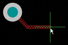
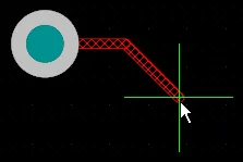
コーナーは短い直線トラックセグメントで定義することも、1 つ以上のアークを使用して作成することもできます。以下の画像は、最も一般的な 2 つのコーナースタイル Track 45 と Any Angle を示しています。

 2 つのコーナースタイル Track 45 と Any Angle の例。画像をクリックすると拡大表示されます。
最初の画像では、インタラクティブルーターが配線の流れに対して全体として直交/斜めパターンを維持している点に注目してください。Any Angle スタイルでは、インタラクティブルーターは開始位置とカーソル位置の間の最短経路を探索します。この配線スタイルは Snake Routing と呼ばれます。
Mitered Corners
最も一般的な配線コーナー形状は、45 度の面取り(斜め)コーナーです。斜めコーナーで配線するには、Track 45 コーナーモードに切り替えます。配線中に誤って直角または鋭角コーナーを作成できないようにするため、インタラクティブ配線とインタラクティブスライドの両方に Miter Ratio オプションがあります。0 以上の正の値を入力します。以下に、同じトレースを Miter Ratio オプションの異なる値で配線した例を示します。
❯ ❮
Javascript ID: InteractiveRouting_MiterRation_AD24_5
|
Miter Ratio に現在のトラック幅を掛けた値が、その miter ratio で配線可能な最もきつい U 字形の壁間隔となります。以下に示します。
-
PCB.ZeroMitersRemoving が Public 状態の場合 – 下の青いボックスから「in Open Beta and」の部分を削除します。
-
PCB.ZeroMitersRemoving が Released 状態の場合 – 下の青いボックス内の「This feature is in Closed Beta」から始まるテキストを削除します。
Miter Ratio を 0 に設定すると、配線またはドラッグ中のトラックで直角または鋭角コーナーを作成できます。この場合、面取りは作成notされません(いわば真のゼロ面取り) – 例を表示。この機能は Open Beta であり、Advanced Settings ダイアログ の PCB.ZeroMitersRemoving オプションが有効な場合に使用できます。このオプションが無効な場合、Miter Ratio = 0 のとき、隣接トレースで完全に覆われる短い面取りが作成されます。
-
Properties パネルで定義された Miter Ratio の値は、インタラクティブ配線、インタラクティブスライド、グロッシングおよびリトレース中に使用されます。
-
インタラクティブ配線およびスライド中に使用される既定の Miter Ratio 値は、Preferences ダイアログの PCB Editor – Interactive Routing ページで設定します。
-
グロッシングおよびリトレース中に使用される既定の Miter Ratio 値は、Preferences ダイアログの PCB Editor – Gloss and Retrace ページで設定します。
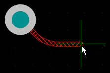
コーナー内のアーク
多くの設計者は曲線コーナーを必要とします。曲線コーナーは、Line 45/90 With Arc コーナーモードまたは Line 90/90 With Arc コーナーモードで配線できます。ただし、Line 90/90 With Arc コーナーモードは 90 度コーナーを強制するため、配線を 45 度方向に継続する必要がある場合は Line 45/90 With Arc コーナーモードを使用してください。アークは配線中に  および
および  キーを使用してインタラクティブにサイズ変更できます(Shift を押し続けるとサイズ変更が加速されます)。
インタラクティブ配線中に曲線コーナースタイルが選択されている場合、グロッシングエンジンは既存の曲線オブジェクトの接線方向パスを優先します。つまり、コーナーを作成するために配置されるアークは、既存オブジェクトの周囲を正確にトレースするように位置と半径が決定されます。これは、たとえば BGA 下のエスケープビアパターンなど、曲線形状が多数存在する領域でスムーズな配線を形成することを目的としています。Routing Gloss Effort が Strong に設定されている場合、アーク間の直線トラックセグメントが水平方向または垂直方向以外の角度で配置されることがあります。
すべての直線トラックセグメントを曲線コーナー付きで完全に水平または垂直に配置する必要がある場合は、斜めコーナーで配線してからグロッシングでコーナーをカーブさせる方が効率的な場合があります。これは、Hugging Style を Rounded に設定し、その後 Retrace Selected コマンドを実行することで実現します。ここでは Gloss Selected ではなく Retrace を使用します。Retrace は経路を短縮したりコーナー数を減らそうとはせず、current design rule settings に従って同じ経路に沿ってグロッシングすることに専念するためです。グロッシングについては後述します。
既存配線のコーナーをカーブさせる。
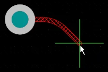
スネーク配線
前述のアークコーナーモードを使用する方法に加えて、コーナースタイルを Any Angle に、Routing Gloss Effort を Strong に設定することで、滑らかに流れるポイントツーポイント配線スタイルを実現することもできます。これがいわゆる Snake Routing です。これは、配線が複数の曲線オブジェクトを通過する任意角度ルートを必要とする場合に使用します。以下の例のビデオに示すとおりです。
コーナースタイルを Any Angle に設定したスネーク配線。
自動接続完了
Interactive Router は、ターゲットパッドへの接続の自動完了(Auto-Complete)を試行できます。Ctrl と Left Click を押し続けると、Interactive Router に現在の接続の完了を試行させることができます。これにより、個々のトラックセグメントを配置するよりもはるかに高速に配線できますが、Auto-Complete 機能には次のような制限があります。
-
開始点とターゲットパッドは同じ層上に存在している必要があります。
-
(配線コンフリクトが無視されていない限り)設計ルールに従ってルートを完了できる必要があります。
Auto-Complete はいつでも使用でき、パッドや接続ライン上でCtrl+clickするだけでそのまま配線できます。事前に選択しておく必要はありません。部分的に配線済みの接続に対しても Auto-Complete を使用できます。その場合は、最後のトラックセグメントの終端、または残っている接続ライン上でCtrl+clickして、ターゲットまで自動で完了させます。
接続を Auto-Complete できない場合、ツールは直前に使用していたインタラクティブ配線モードに戻ります。
サブネットジャンパー
FPGA ベース設計の大きな強みの 1 つは、配線の課題を PCB と FPGA の両方で解決できるため、配線層数の削減や PCB の単純化につながる可能性があることです。これを実現するには、設計システムが PCB 主導および FPGA 主導のピンスワップの両方をサポートする必要があります。Altium Designer は PCB エディタでのピンスワップをサポートしており、単純な 2 ピン部品から高ピン数 FPGA まで対応します。
設計プロセスの任意の段階(配線済み PCB 上も含む)でのピンスワップをサポートするため、PCB エディタは subnet jumpers と呼ばれる小さな配線コネクタを追加・削除できます。サブネットジャンパーは、ソフトウェアが簡単に配置・削除できる要素として認識する短いトラックセグメントです。これは、Add および Remove Subnet Jumper コマンドを Route メニューから手動で実行するか、インタラクティブ配線中にスワップ可能なピンへ配線した場合には配線エンジンによって自動的に追加・削除されます。
❯ ❮
Javascript ID: SubnetJumpers
|
|
|
手動で配置するサブネットジャンパー
ネットに短い接続ラインが残っている場合、Route » Add Subnet Jumpers コマンドを実行して配線を完了できます。このコマンドを実行すると、下図のような Subnet Connector ダイアログが表示されます。ダイアログに値を入力して Run ボタンをクリックすると、ボード上のすべての接続ラインがチェックされ、その長さが Maximum Subnet Separation で指定した長さ以下のものはトラックセグメントに置き換えられます。このトラックセグメントの幅は、接続される 2 つのセグメントのうち狭い方の幅になります。なお、サブネットジャンパーが配置される角度は、接続ラインの両端点の位置によって決まります。
 サブネットジャンパーに許可する最大長を指定します。
-
Route » Remove All Subnet Jumpers コマンドを実行して、ボード上の既存のサブネットジャンパーをすべて削除します。
-
Add および Remove Subnet Jumpers コマンドをサポートするために、既存の配線を分割するには Edit » Slice Tracks command を使用できます。
インタラクティブ配線中に配置されるサブネットジャンパー
配線中のネットがスワップ可能に設定されている場合、配線エンジンはすべての潜在的な配線ターゲットを認識してハイライト表示します。既存のトラックセグメント(パッドではなく)に向かって配線しているときに、同一ネットのトラックセグメントではなくスワップ可能なトラックセグメントをターゲットとして選択すると、インタラクティブ配線エンジンは自動的にサブネットジャンパーを追加します。これは下のビデオで示されています。
ターゲットが同一ネットの経路ではなくスワップ可能な経路である場合、インタラクティブ配線中にサブネットジャンパーが自動的に追加されます。
サブネットジャンパーを標準トラックに変換する
サブネットジャンパーを通常のトラックセグメントに変換するには、その上でマウスボタンを短くクリック&ホールドし、そのままマウスを動かさずにボタンを離します。すると、サブネットジャンパーは標準トラックセグメントに置き換えられます(上記ビデオの終盤を参照)。同じ操作で複数のサブネットジャンパーを一度に変換するには、まず対象のサブネットジャンパーを選択し、そのうちの 1 つ上でクリック&ホールドします。ボード上のすべてのサブネットジャンパーを選択するには、Select チェックボックスを有効にした状態で PCB Filter パネル内でクエリ IsSubnetJumper を実行します。
インタラクティブ配線およびインタラクティブスライドのオプション
接続をインタラクティブに配線している場合でも、既存の配線をドラッグして新たな配線スペースを確保している場合でも、同じ一連の配線技術が適用されます。このセクションでは、Interactive Routing および Interactive Sliding モードの Properties パネルで利用できるオプションをまとめます。これらの多くのオプションのデフォルト設定は、Preferences ダイアログの PCB Editor – Interactive Routing ページで構成します。
Interactive Routing and Interactive Sliding Options
Gloss Effort (Routed)
インタラクティブ配線、インタラクティブスライド、ActiveRouting などのルートイベント中、ソフトウェアはグロッシングエンジンを実行します。グロッシングエンジンは、現在のルートイベントで配置または影響を受けたすべてのセグメントを継続的に見直し、結果の品質向上を試みます。品質の指標には、コーナー数の削減、セグメント数の削減、鋭角の除去、全体の配線長の短縮などがあります。
グロッシングには Off、Weak、Strong の 3 つの設定があります。これらの設定については Glossing – Smoothing the Routes セクションで説明します。
Gloss Effort (Neighbor)
Gloss Effort (Neighbor) は、現在のインタラクティブ配線またはスライドによって影響を受ける隣接配線に対して適用されるグロッシング量を設定します。これも Off、Weak、Strong の 3 つの設定があります。
Hugging Style
このオプションは、インタラクティブスライド中のコーナー形状の扱いを制御し、スライドされるトラックと押されるトラックの両方に影響します。スライド中に Shift+Spacebar ショートカットを使用して 3 つのモードを切り替えます。
-
45 Degree – スライド中のコーナー生成には常に直線の直交/斜めセグメントを使用します(従来の直交/斜め配線動作に使用します)。
-
Mixed – 移動/押し当てる対象が直線の場合は直線トラックセグメントを、曲線の場合はアークを使用します。
-
Rounded – 移動/押し当ての対象となる各頂点でアークを使用して曲線コーナーを形成します。スネーク配線や、グロッシング時(インタラクティブ配線および手動グロッシング中)にアーク+任意角度配線を使用する場合にこのモードを使用します。
インタラクティブスライド中のトラック移動によって影響を受ける既存のコーナーは、現在の Hugging Style に基づいて(45 Degree から Rounded、または Rounded から 45 Degree へ)変換されます。
Conflict Resolution
このオプションは、既存オブジェクトに遭遇したときに配線/スライド中のオブジェクトをどのように動作させるかを決定します。配線またはスライド中に Shift+R ショートカットを使用して利用可能なモードを切り替えます。
これらのモードは、PCB Editor – Interactive Routing ダイアログの PCB Editor – Interactive Routing ページで Routing Conflict Resolution modes として参照されます。
Vertex Action
既存配線の容易な操作と再成形という設計者のニーズをより良くサポートするため、トラックやアークではなく頂点(2 つのセグメントが交わるコーナー位置)をクリック&ドラッグした場合に適用される特定のオプションがあります。スライド中に Spacebar ショートカットを使用して利用可能なモードを切り替えます。
-
Deform – 移動中の頂点に接続されたトラックセグメントを分割または延長し、頂点がカーソルの動きに追従するようにします。
-
Scale – コーナー形状を保持したまま、頂点をカーソルに追従させつつ、流入側トラックセグメントのサイズ変更と移動を行います。
-
Smooth – コーナーを滑らかに再成形し、スライド処理で影響を受けるすべての頂点で、内側にドラッグしたときにアークを挿入して曲線コーナーを作成します(Mixed または Rounded の Hugging Style 時)。Rounded Hugging Style では外側にドラッグした場合にもアークを追加します。
チェックボックスオプション
-
Automatically Terminate Routing – 現在配線中の接続がターゲットパッドに到達したとき、そのネットの配線を自動的に終了しますが、Interactive Routing コマンドは継続し、別のネットの配線をすぐに開始できるようにします。
-
Automatically Remove Loops – このオプションを有効にすると、既存配線に対して新しい経路を引くことができます。新しい経路が既存経路に戻って合流すると、冗長なループは自動的に削除されます。詳細は Modifying Existing Routes を参照してください。
-
Remove Net Antennas – ネットアンテナとは、短い終端されていないトラック(アーク)セグメントのことです。現在の配線がアンテナが接触しているオブジェクトに影響を与えた場合、これらは自動的に削除されます。
-
Allow Via Pushing – Push または Hug & Push モードでの配線/スライド中に、既存ビアも押し出し可能にします。
-
Display Clearance Boundaries – 適用される Clearance デザインルールによって定義される、既存オブジェクトの周囲の進入禁止領域を表示します。
-
Reduce Clearance Display Area – この表示を、現在のカーソル位置の周囲にある円形ゾーンに縮小します。
-
Show Length Gauge – 長さゲージは、現在の配線が適用される Length および Matched Length デザインルールをどの程度満たしているかを示します。詳細は Length Tuning を参照してください。
Pad Entry Stability
Pad Entry Stability スライダーは、センターに入っているパッドへのエントリを保護し、グロッシングによってセンターに入っているトラックがセンターからずれないようにします(センターにあるトラックをセンターに保持するだけであり、センターから外れているトラックをセンターに合わせることはしません)。スライダーバーを使用して保護レベルを設定します。
Trace Centering
Trace Centering 機能は、Apply Trace Centering オプションが有効な場合に、配線中またはドラッグ中のネットと既存のパッド/ビアとの間に、可能な限り追加のクリアランスを設けます。オプションを有効にすると、次のオプションを使用して機能を設定できます。
トレースをインタラクティブにスライドするときにトレースセンタリングを無効にするには、Disable Trace Centering When Dragging オプションを使用します。このオプションは、Dragging 領域の PCB Editor – Interactive Routing ページ(Preferences ダイアログ内)か、インタラクティブスライド用の Properties 領域(Properties パネル内)で設定できます。このオプションが有効な場合、機能のメイン Apply Trace Centering オプションが有効であっても、トレースのインタラクティブスライド中にはトレースセンタリングは適用されません。
Trace Centering についてさらに詳しく学ぶ。
Miter Ratio
Miter Ratio はコーナーの最小のきつさを制御します。Miter Ratio に現在のトラック幅を掛けた値が、その比率で配線可能な最もきつい U 字形の壁間隔になります。この関係は、このページ前半の Mitered Corners の説明に示されています。0 以上の正の値を入力します(x 乗数は自動的に追加されます)。
Min Arc Ratio
Min Arc Ratio は、任意角度インタラクティブ配線中および Mixed ハギングスタイルでのインタラクティブスライド中に適用されます。この比率は許容される最小半径のアークを決定するために使用され、アーク半径がこの最小値を下回ると、そのアークはトラックセグメントに置き換えられます。条件は次のとおりです。
Min Arc Radius = Min Arc Ratio x Arc Width
-
この設定は、コーナーでのアーク配線中や Rounded ハギングスタイルでのインタラクティブスライド中には適用されません。これらのモードではセグメント化されたアークを使用しないためです。
-
Minimum Arc Ratio を 0(ゼロ)に設定すると、常にアークが使用されます。
Modifying Existing Routes
Glossing – 配線のスムージング
最小限のコーナー数で整然とした配線を行えるように、PCB エディタには Glossing ツールが用意されています。Glossing は、適用される設計ルールの意図を尊重しつつ、よりクリーンな配線とパッドエントリを生成するために特別に開発された高度なアルゴリズム群です。Glossing はパス長の短縮、コーナー形状の改善と数の削減を試み、一般的にセグメント数の少ない、より整った配線を生成します。また、Glossing はサブネットジャンパーはそのまま残し、ルームベースの幅ルールがある場合には境界での幅変更を尊重します。カーソルを動かして新しいインタラクティブルートパスを定義している間、まだ確定していない配線も自動的に Glossing が適用されます。
Glossing エンジンには Retrace Selected コマンドも含まれています。これは、配線ルールの設定を変更した内容を選択済みの配線に反映させたいときに使用します。Retrace を使うことで、選択した電源配線を「太らせる」ことや、選択した差動ペアを新しい幅とギャップ設定に更新することができます。
Glossing は、インタラクティブ配線、インタラクティブスライド、および Gloss Selected または Retrace Selected コマンドの実行時に適用されます。
Glossing には Off、Weak、Strong の 3 つの設定があります。インタラクティブ配線またはインタラクティブスライド中に Ctrl+Shift+G ショートカットを使用して設定を順送りするか、Tab を押して Properties パネルを開き、設定を選択します。
-
Off – このモードでは、Glossing は実質的に無効になります。ただし、配線/ドラッグ後には、重なり合うトラックセグメントを除去するなどのクリーンアップ処理は引き続き実行されます。このモードは、トラックの手動ドラッグやパッドエントリのクリーンアップなど、基板レイアウトの最終段階で細かな調整を行う際に有用です。
-
Weak – このモードでは、低レベルの Glossing が適用されます。インタラクティブルータは、現在配線しているトラック(またはドラッグされているトラック/ビア)に直接接続されている、あるいはその周辺にあるトラックのみを考慮します。言い換えると、トレースの形状は主に保持され、局所的にスムージングされます。このモードの Glossing は、トラックレイアウトの微調整やクリティカルな配線を扱う場合に有用です。
-
Strong – このモードでは、高レベルの Glossing が適用され、インタラクティブルータは最短経路の探索やトラックのスムージングなどを積極的に行います。このモードの Glossing は、基板レイアウトの初期段階で、できるだけ多くの配線を短時間で完了させたい場合に有用です。Strong Glossing がコーナーでのアークモードのいずれかと組み合わされている場合、任意角度のトレースも許可される点に注意してください。ここでは、設計者がコーナーを曲線化しているので、コーナー間の非直交配線にも抵抗がないだろうという前提に基づいています。
現在の Gloss Effort 設定に加えて、Glossing は次の設定にも従います。
-
Corner Style
-
Hugging Style(インタラクティブスライド中および Gloss Selected / Retrace Selected コマンド実行時)
-
Miter Ratio
-
Min Arc Ratio
これらのオプションを使用して、Glossing はコーナーをどれだけタイトに生成するか、および曲線状の障害物の周囲でルートの曲線形状をどのように形成するかを制御します。
インタラクティブ配線またはスライド中の Glossing の強さは、次の 2 つのオプションで制御します。現在配置またはドラッグしているルートに対する Gloss Effort (Routed) と、現在のインタラクティブ配線またはスライドによって影響を受ける隣接ルートに対する Gloss Effort (Neighbor) です。これらのオプションに対する異なる Gloss Effort モードの例を以下に示します。
❯ ❮
Javascript ID: InteractiveRouting_GlossEffortRouted_AD24
|
❯ ❮
Javascript ID: InteractiveRouting_GlossEffortNeighbor_AD24
|
既存の配線は、Route » Gloss Selected コマンドを実行することで Glossing できます。Corner Style を事前に設定しておくことで、マイターコーナーをアークに変換するなどの設計変更を行う際に有効活用できます。
Glossing & Retracing of Existing Routes
Temporarily Inhibit Glossing – Glossing はインタラクティブ配線およびスライドの中核機能ですが、望む配線形状の実現を妨げる場合もあります。そのような場合には、Ctrl+Shift ショートカットキーを押し続けることで、一時的に Glossing を抑制できます。キーを離すと、現在の設定で Glossing が再度有効になります。
Gloss の実行
Glossing ツールは次のように実行されます。
-
During Interactive Routing – PCB Editor – Interactive Routing ページ(Preferences ダイアログ内)または Interactive Routing mode(Properties パネル内)で定義された現在の Gloss 設定に従って実行されます。
-
During Interactive Sliding – PCB Editor – Interactive Routing ページ(Preferences ダイアログ内)または Interactive Sliding mode(Properties パネル内)で定義された現在の Gloss 設定に従って実行されます。
-
現在選択されている配線に対して – メニューから Route » Gloss Selected コマンドを選択するか、Ctrl+Alt+G キーボードショートカットを押して、PCB Editor – Gloss and Retrace ページ(Preferences ダイアログ内)または Gloss And Retrace パネル で定義された Gloss 設定に従って Gloss を実行します。
-
After ActiveRoute – Gloss Results オプションを PCB ActiveRoute パネル で有効にします。
Inhibit Glossing During Routing and Sliding
一時的に Glossing をオフにしたい場合もあります。Glossing は Ctrl+Shift ショートカットキーを押し続けることで抑制できます。キーを離すと、Routing Gloss Effort の現在の設定で Glossing が再開されます。ステータスバーにはこの一時的な状態は反映されず、最後に選択された状態が表示され続ける点に注意してください。
Glossing Options
Gloss Effort (Routed)
ルートに対してどの程度強く Glossing を行うかは、現在の Gloss Effort (Routed) 設定で制御されます。このオプションは Interactive Routing ページ(Preferences ダイアログ内)で設定するか、Ctrl+Shift+G ショートカットを使用して 3 つのモードを順送りで切り替えます。現在の設定はステータスバーに表示されます。(show image )
)
-
Off – このモードでは、Glossing は実質的に無効になります。ただし、配線/ドラッグ後には、重なり合うトラックセグメントを除去するなどのクリーンアップ処理は引き続き実行されます。このモードは、トラックの手動ドラッグやパッドエントリのクリーンアップなど、基板レイアウトの最終段階で細かな調整を行う際に有用です。
-
Weak – このモードでは、低レベルの Glossing が適用されます。インタラクティブルータは、現在配線しているトラック(またはドラッグされているトラック/ビア)に直接接続されている、あるいはその周辺にあるトラックのみを考慮します。このモードの Glossing は、トラックレイアウトの微調整やクリティカルなトレースを扱う場合に有用です。
-
Strong – このモードでは、高レベルの Glossing が適用され、最短経路に強く重点が置かれます。このモードの Glossing は、基板レイアウトの初期段階で、基板の大部分を短時間で配線したい場合に有用です。
Gloss Effort (Neighbor)
Gloss Effort (Neighbor) は、現在のインタラクティブ配線またはスライドによって影響を受ける隣接ルートに対して適用される Glossing の量を設定します。Off、Weak、Strong の 3 つの設定があります。
Hugging Style
このオプションは、Glossing 中にコーナー形状をどのように処理するかを制御します。Glossing は、現在の編集操作によって影響を受けるすべてのトラックセグメントに適用されるため、周囲のトラックにも影響を与える可能性があります。たとえば、プッシュモードでのインタラクティブ配線やインタラクティブスライド中には、スライドされているトラックと押されているトラックの両方に対して、現在の Hugging Style 設定に従って Glossing が適用されます。
-
45 Degree – コーナーの生成には常に直交/斜めの直線セグメントのみを使用します(従来の直交/斜め配線動作を行いたい場合に使用します)。
-
Mixed – 移動/プッシュ対象が直線の場合は直線トラックセグメントを使用し、曲線の場合はアークを使用します。
-
Rounded – グロス処理される各頂点でアークを使用します。スネーク配線時や、グロス処理中(インタラクティブ配線および手動グロス処理時)にアーク+任意角度配線を使用する場合に、このモードを使用します。
Minimum Arc Ratio
Minimum Arc Ratio は、任意角度インタラクティブ配線中および Mixed Hugging Style を使用したインタラクティブスライド中に適用されます。この比率は許容される最小半径アークを決定するために使用され、アーク半径がこの最小値を下回ると、そのアークはトラックセグメントに置き換えられます。ここで:
Min Arc Radius = Min Arc Ratio x Arc Width
-
この設定は、コーナーでのアーク配線や、Rounded Hugging Style を使用したインタラクティブスライド中には適用されません。これらのモードではセグメント化されたアークを使用しないためです。
-
常にアークを使用するには、Minimum Arc Ratio を 0(ゼロ)に設定します。
Miter Ratio
Miter Ratio はコーナーの最小のきつさを制御します。Miter Ratio に現在のトラック幅を掛けた値が、その比率で配線可能な最もきつい U 字形の壁間隔になります。Mitered Corners について詳しく学ぶことができます。
Pad Entry Stability
Pad Entry Stability スライダーは、パッド中央への進入を保護します。これはグロス処理中に、すでに中央にあるパッド進入(退出)を保護するために適用され、オフセンターになっている既存のパッド進入を再センタリングしようとはしません。
-
0 (Off) = 保護なし
-
10 (Max) = 最大保護
Pad Entry Stability 機能のデモンストレーション。
言い換えると、このオプションは、パッド進入を横方向にシフトすることを許可するために、配線コーナーがパッドエッジにどれだけ近づく必要があるかをグロスエンジンに指示します。
最大保護を選択すると、パッドエッジで鋭角が生じる場合があることに注意してください。
配線中に配線幅とビアサイズを制御する
Interactive Routing コマンドを実行してクリックし、配線を開始すると、最寄りのパッドから現在のカーソル位置まで一連のトラックオブジェクトが作成されます。これらのトラックの幅は、配線中にステータスバーに表示される現在の Track Width Mode 設定によって決定されます(下のビデオを参照)。
Routing Width Source の設定には、次の 4 つの可能性があります:
-
設計者が好む幅(User Choice と呼ばれます。これは、該当する Routing Width デザインルールで許可される範囲内でなければなりません)、または
-
該当する Routing Width デザインルール の Minimum、Preferred、または Maximum の値。
User Choice / Min rule / Preferred rule / Max rule の選択は、Preferences ダイアログの PCB Editor – Interactive Routing ページにある Track Width Mode ドロップダウン で保存および選択できます。
配線中に Track Width Mode を変更する
インタラクティブ配線中に 3 ショートカットキーを押すことで、4 つの配線幅オプションを順送りに切り替えることができます(下のビデオ参照)。現在のモードはステータスバーに表示されます。コマンド中のショートカットを忘れた場合は、コマンド実行中に Shift+F1 を押して一覧を表示します。
配線中にトラック幅のソースを変更するには、キーボードの 3 キーを押します。Shift+W を押して User Width の別の値を選択します。
トラック幅モードを変更すると、該当するデザインルールで定義された値(Min/Preferred/Max)と User Choice の間を移動します。
User Choice を選択した場合、トラック幅は次のようになります:
配線中に User Choice の配線幅を変更する
配線中に幅を変更するには、次のショートカットを使用します。なお、Interactive Routing Width Sources オプションがルールベースの幅オプションのいずれかに設定されている場合、これらのショートカットを使用すると、そのオプションは User Choice に変更されます。
-
Shift+W – 配線中にこのショートカットを使用すると、Choose Width ダイアログが開きます。新しい幅をクリックすると、ダイアログが閉じ、選択した幅で配線を続行します。利用可能な幅は、PCB Editor – Interactive Routing ページの Preferences ダイアログ内にある Favorite Interactive Routing Widths ボタンをクリックして開く Favorite Interactive Routing Widths ダイアログ で編集するか、PCB エディタのデザインスペースで O キーボードショートカットを使用し、その後のポップアップメニューで Favorite Routing Widths エントリを選択して編集できます。
-
Tab – 必要な幅がお気に入りとして定義されていない場合にこのショートカットを使用します。Tab を押すと、Interactive Routing モードで Properties パネルを開きます。現在の編集セッションはいったん一時停止し、現在の Width が選択された状態でパネルが開きます。新しい幅の値を入力し、Enter を押して新しい幅で配線を続行します。あるいは、新しい幅の値を入力後、一時停止ボタンのオーバーレイをクリックして配線を再開します。値を編集せずに配線を再開するには、Esc を押します。
これらの手法のいずれかを使用して配線中に幅を変更した場合、Track Width Mode は自動的に User Choice に変更されることを忘れないでください。
配線トラック幅は、該当する Routing Width デザインルールで指定された最小値と最大値の間でなければなりません。ルールの Minimum および Maximum 設定で定義された範囲外の値に幅を変更しようとすると、ソフトウェアは自動的にその値を Min-Max 範囲内にクリップします。
配線中にレイヤーを変更する
インタラクティブに配線中のレイヤーを変更するには、次の 2 つの方法があります:
-
テンキーの * キーを押します。このキーを押すたびに、次に利用可能なシグナルレイヤーへと下がっていきます。
-
Ctrl+Shift+Wheel Scroll ショートカットの組み合わせを使用します。Ctrl+Shift キーを押しながらマウスホイールを前方にスクロールすると、利用可能なシグナルレイヤーを down 方向に移動し、後方にスクロールすると、利用可能なシグナルレイヤーを up 方向に移動します。このショートカットは、いつでもレイヤーを変更するために使用できることに注意してください。現在配線していない場合、このショートカットの組み合わせは有効なすべてのレイヤーを順送りに切り替えます。
ビアは、最後の 2 つのセグメントが交わる最後のコーナーに自動的に追加されます。配線幅と同様に、ビアのサイズは、下のビデオに示す現在の Via Size Mode によって決定されます。このモードは、 Interactive Routing Width Sources オプションで事前に設定できます。
Ctrl+Shift+Scroll ショートカットを使用してレイヤーを変更し、4 ショートカットキーを使用してビアサイズの選択肢を順送りに切り替えます。
配線中に Via Size Mode を変更する
配線幅と同様に、インタラクティブ配線中にビアサイズを選択するためのオプションは 4 つあります:
-
設計者が好むビアサイズ(User Choice)、または
-
該当する Routing Via Style デザインルールの Minimum、Preferred、または Maximum の値。
インタラクティブ配線中に 4 ショートカットキーを押すことで、4 つのビアサイズオプションを順送りに切り替えることができます。現在のモードは、上のビデオに示すようにステータスバーに表示されます。
配線中に User Choice のビアサイズを変更する
配線中に User Choice のビアサイズを変更するには:
-
Shift+V – インタラクティブ配線中にこのショートカットを押して Choose Via Size ダイアログを開きます。このダイアログには、現在デザインで使用されているすべてのビアサイズが自動的に一覧表示されます。ビアサイズを選択し、OK をクリックして、それを User Choice ビアサイズにします。

-
Tab – 配線中のトラック幅を変更するだけでなく、Tab を押して Properties パネルを Interactive Routing モードで開くと、Via Diameter も変更できます。トラック幅と同様に、入力するサイズは、該当する Routing Via Style デザインルールで定義された最小値と最大値の間でなければなりません。
配線中に Via Type を変更する
複数の Via Type が定義されている場合、レイヤー変更時に、スパンされるレイヤーに対して複数の Via Type が利用可能なことがあります。例えば、top と mid1 レイヤー間にブラインドビアが利用可能で、同時に top-bottom の Via Type も利用可能な場合です。レイヤー変更を行っていて、利用可能な Via Type が複数ある場合、6 ショートカットを押して利用可能な Via Type オプションを順送りに切り替えることができます(または 8 ショートカットを押して一覧を表示します)。詳細については、Defining the Via Types ページを参照してください。さらに、最後に使用したビアスタックは、次に配線するネットのデフォルトとして保持されます。デフォルトのビアスタックは、現在の編集セッション中のみ保持されます。

L1 から L4 へのレイヤー変更中に配置されるスタックド µVia。Properties パネルの Interactive Routing モードには、配置される Via Type が表示されます。6 を押して利用可能なビアスタックを順送りに切り替え、8 を押して利用可能なビアスタックの一覧を表示します。
Look Ahead Routing Segment 使用時のビアの挙動
インタラクティブ配線中、まだ配置されていないトラックセグメントはハッチ表示され、確定済みのセグメントは実線で表示されます。別のモードとして、カーソルに接続された最後のセグメントが中抜き(アウトライン)で表示されるモードがあり、このセグメントは「ルックアヘッドセグメント」と呼ばれます。ルックアヘッドモードで配線している場合、クリックするとハッチ表示のセグメントはすべて配置されますが、中抜きのセグメントは配置されません。最後のセグメントを確定せずに、その直前のセグメントを正確に配置できるようにするための機能です。配線中に 1 ショートカットキーを押すと、ルックアヘッドモードをオン/オフ切り替えできます。
レイヤー変更中にルックアヘッドモードをオンに切り替えると、クリックしてもルックアヘッドセグメントは配置されないため、ビアはカーソル位置から直前のコーナー位置へとジャンプします。以下のビデオでこの挙動を確認できます。
 レイヤー変更中に 1 キーを押してルックアヘッドモードをオン/オフすると、ビアは最後の配置準備済みセグメントの終端位置にジャンプします。
SMD パッドへのエントリ制御
SMD To Corner および SMD Entry デザインルールは、配線プロセスに影響を与える可能性があります。トラックが SMD パッドにどのように進入・退出するかを制御できるように、配線を開始する前に必要なデザインルールを設定しておく必要があります。PCB Rules and Constraints Editor ダイアログ(メインメニューから Design » Rules をクリック)を開き、これらのデザインルールを作成・設定します。

SMD to Corner デザインルールでは、「distance to corner」の値は、トラック幅または適用されるクリアランスルール(大きい方)の値より大きくする必要があります。やむを得ずそれより小さくする必要がある場合は、次の 3 つの方法で対処できます。
-
パッドエントリを行っている間に Spacebar を押します。これにより、最後のトラックセグメントをパッド中心に沿って整列させるのに役立ちます。
-
パッドの近くで配線を確定し、その後グロス処理なしでパッドエントリを行います(グロス処理は Ctrl+Shift を押し続けることで一時的に無効化できます)。
-
複数の進入パスが可能な状態でパッドエントリを行う場合、マウスをパッド内部に移動します。これにより、SMD エントリ位置を任意に選択できます。
SMD Entry ルールにおいて、パッドの「Side」とは長辺側を指します。デザインルールの Side オプションは、パッドが SideLength > 2 * EndLength の場合にのみ適用されます。これは、多くの SMD ディスクリート部品のパッドがほぼ正方形であり、これらのデバイスではパッドのどの辺からでも配線できるようにしておくことが望ましいためです。
トレースセンタリング
多くの設計者が望む一般的な要件として、可能な限り、パッドやビアの間を通過するトレースを中央に配置したいというものがあります。現在の配線エンジンの動作は、デザインルールで定義された最小許容クリアランスでトラックセグメントを配置し、パッド間でのトレースの拡張やセンタリングは後から行う、というものです。
トレースセンタリング機能は、配線中またはドラッグ中のネットと既存のパッド/ビアとの間に追加クリアランスを設けることで、このセンタリング処理を支援します。配線エンジンは、この追加クリアランスが「必須」ではなく「望ましい」ものであることを理解しているため、例えば 2 本目や 3 本目のトレースを既存のパッド/ビア間に押し込む必要がある場合などには、この追加分の一部または全部を取り戻すことができます。配線エンジンがクリアランスを削減する必要がある場合は、可能な限りトレースが中央に保たれるよう、両側から均等に削減します。
トレースセンタリングの挙動は、PCB Editor – Interactive Routing ページ のオプションおよびインタラクティブ配線中の Preferences ダイアログと Properties パネルで設定できます。

Preferences ダイアログでのインタラクティブ配線用トレースセンタリングオプション

Properties パネルでのインタラクティブ配線用トレースセンタリングオプション
パッドおよびビアの周囲に追加クリアランスを設けることで、トレースを中央に配置できます。
-
この機能は Any Angle を含むすべての配線モードで利用できます。また、インタラクティブ差動ペア配線 および インタラクティブスライド 中でも利用できます。
-
トレースをインタラクティブにスライドする際にトレースセンタリングを無効にするには、Disable Trace Centering When Dragging オプションを Dragging 領域の PCB Editor – Interactive Routing ページ(Preferences ダイアログ内)またはインタラクティブスライド用の Properties 領域(Properties パネル内)で使用します。このオプションが有効な場合、機能のメイン Apply Trace Centering オプションが有効であっても、トレースのインタラクティブスライド中にはトレースセンタリングは適用されません。
配線の自動シュリンク
インタラクティブルーターで配線しているトレースが、現在選択されている配線幅では障害物の間を通過できない場合、自動シュリンク機能により、その場所でトレースを通せる幅まで自動的に幅を縮小できます(ただし、この縮小後のトレース幅が、対応する制約で定義された最小許容幅を下回らないことが条件です)。この機能を有効にするには、Auto Shrinking オプションを PCB Editor – Interactive Routing ページ の Preferences ダイアログおよび Properties パネルで有効にし、インタラクティブ配線 中に使用します。
配線中に自動的に配線幅を変更する
最新のコンポーネント技術では、ボード上を配線していく中でネットの幅を変える必要がある、という課題がよく発生します。例えば、BGA への進入/退出では、BGA フットプリントの外周付近で推奨幅に切り替える前に、より細いエスケープルートが必要になることがよくあります。
これは、このページで前述したテクニックを用いてインタラクティブ配線中に手動で行うこともできますが、プレースメントルームとルームベースの配線幅ルールを追加することで、この幅切り替え動作を自動化することもできます。これを設定すると、ルームに入る/出る際にトラックが自動的にネックダウンおよび拡張されます。
この機能は次のように動作します。
これらの設定が完了すると、以下のビデオに示すように、プレースメントルームに入る/出る際に幅が自動的に切り替わります。


ルーム境界を横切る際、幅ルールが順守され、トラックセグメントはインテリジェントにサイズ変更されます。
ルームベースの配線を行うには、まずプレースメントルームを定義する必要があります。プレースメントルームもデザインルールの一種です。デザインルールダイアログからルールを作成してルームを定義することもできますが、逆にルームをインタラクティブに作成し、Altium Designer にデザインルールを自動生成させた方が効率的な場合もあります。
ルームルールの作成
Design » Rooms サブメニューには、複数のルーム定義コマンドがあります。
 ルームは、コンポーネントの配置位置を制御したり、そのボード領域内で適用されるルールを制御したりするのに便利な機能です。
選択したコンポーネントの周囲にルームを作成すると、次のことが行われます。
-
選択したコンポーネントからコンポーネントクラスが作成されます。クラス(Design » Classes)を確認し、必要に応じてコンポーネントクラス Name を更新します。
-
Placement Room Definition デザインルールが作成されます。このルールは、ステップ 1 で作成されたコンポーネントクラスをターゲットとするようスコープ設定されています。コンポーネントクラス名を変更した場合は、ルールスコープ(Full Query)もそれに合わせて更新する必要があります。
-
Placement Room Definition デザインルールには自動的に名前が付けられます。必要に応じて名前を変更し、その名前を控えておきます。ルームは他のデザインルールからその Name によって参照されるためです。
-
必要に応じてルームのサイズを変更します。これを行うには、まず一度クリックしてルームを選択し、次に頂点をクリック&ホールドしてコーナーまたはエッジを移動します。頂点をクリックして移動する際に Shift を押すと、対称リサイズを行うこともできます。
をターゲットとするようスコープ設定されています。") この例では、ルールはコンポーネントクラスではなく、特定の BGA フットプリント(「BGA50P18X18-180」)をターゲットとするようスコープ設定されています。
この例では、ルールはコンポーネントクラスではなく、特定の BGA フットプリント(「BGA50P18X18-180」)をターゲットとするようスコープ設定されています。
配置ルーム定義デザインルールは、通常 1 つ以上のコンポーネントを対象とするようにスコープ設定されます。ここで説明しているように、そのルームで定義された領域内の配線を制御する目的で使用する場合、必ずしも特定のコンポーネントを対象にスコープ設定する必要はありません。例えば、ルールのスコープ (Full Query) を All に設定しても、配線動作は要求どおりになります。ルーム内のコンポーネントを対象にスコープ設定する利点は、コンポーネントを移動する必要が生じたときに、Design » Rooms » Move Room コマンドを使用してルームとコンポーネントを一緒に移動できる点です。
ルームベースの配線ルールの作成
異なる配線幅が必要な領域を定義するルームを作成したら、その配線幅ルールを作成できます。下図は、Room_BGA という名前のルームに配線が触れたときに、PCB エディタに配線幅を 0.075mm に設定するよう指示するようスコープ設定された Routing Width ルールの例です。Altium Designer のインタラクティブルータエンジンは、このようなルールを満たすために、ルーム境界で現在のトラックセグメントを自動的に終了し、新しいセグメントを開始します。

ルーム Room_BGA 内のすべてのネットの幅を 0.075mm に設定するようスコープ設定された Routing Width デザインルール。ツリーの先頭に表示されていることから、これが最優先の配線幅ルールであることが分かります。
TouchesRoom および WithinRoom クエリキーワードの詳細
Net Tie コンポーネントを使用した 2 つのネットの接続
意図的に 2 つの異なるネットを接続する必要が生じることは珍しくありません。例えば、アナログ GND とデジタル GND を制御された方法で接続する必要がある場合などです。これは、2 つのネットを Net Tie コンポーネントで接続することで実現します。Net Tie コンポーネントは、制御されたショート回路にほかならず、基板上でネット同士を接続する位置をユーザーが決定できるようにするものです。
Net Tie パッドに向かって配線する際の課題は、ルールエンジンが違反が発生しようとしていることを検出し、Net Tie パッドへの配線を妨げてしまう点です。
-
これを解決するには、Routing Mode を
Ignore Obstacle に切り替えます。
Net Tie に向かって配線するには、Routing Mode を Ignore Obstacle に切り替えます。
意図的に 2 つのネットを接続する
の詳細
インタラクティブルータの Follow モードで既存形状に沿ってトレースする
配線中によくある要件として、既存の形状や輪郭に沿うように配線を配置したい場合があります。輪郭は、障害物、カットアウト、ボードエッジ、あるいは既存の配線であることもあります。
輪郭に「対抗」するように、マウス操作とクリックを慎重かつ正確に行って新しい配線を輪郭に密着させる代わりに、Follow モードでは、輪郭をクリックして指定し、その輪郭に沿ってカーソルを動かすことで配線方向を定義します。Follow モードでは、インタラクティブルータがトラックおよびアークセグメントを追加し、適用されるデザインルールに準拠しながら新しい配線が輪郭に沿うようにします。この機能は、特に曲線配線を行う際に有用です。
この機能を使用するには:
-
インタラクティブ配線を起動し、配線する接続をクリックして選択し、必要なコーナースタイル (Shift+Spacebar) に切り替えます。
-
輪郭に沿って配線するには、対象オブジェクト上にカーソルを置き、Shift+F を押します。インタラクティブルータはカーソル下のオブジェクトを検出し、Follow モードに切り替わります。
-
必要な方向にカーソルを動かします。ソフトウェアは、その方向の輪郭に沿うようにトラックおよびアークセグメントを自動的に配置します。
-
Left-click を押して Follow セグメントを配置し、Follow モードを終了します。
-
必要に応じて配線を完了します。
利用可能な配線コンフリクト解決モード
前述のとおり、インタラクティブルータが、他ネットのパッドなど PCB ワークスペース内に既に存在するオブジェクトにどのように応答するかは、現在の Routing Conflict Resolution モードに依存します。配線中に利用可能なコンフリクト解決モードは、Preferences ダイアログのPCB Editor – Interactive Routing ページで設定します。
コンフリクト解決モードには次のものがあります:
-
Ignore Obstacles – 既存オブジェクトを無視します(配線は自由に配置でき、配線中にトラックを障害物の上に通すことができます)。違反はハイライト表示されます。
-
Push Obstacles – 既存のトラックやビアを押しのけて、新しい配線のためのスペースを確保します。このモードで障害物を押しのけると違反が発生する場合は、配線がブロックされていることを示すインジケータが表示されます。
-
Walkaround Obstacles – トラック、パッド、ビアなど既存オブジェクトの周囲に経路を見つけようとします。他オブジェクトとのクリアランスは、該当する Clearance デザインルールで定義されます。このモードで障害物を回避すると違反が発生する場合は、配線がブロックされていることを示すインジケータが表示されます。
-
Stop At First Obstacle – このモードでは、配線エンジンは最初に遭遇した障害物で停止します。
-
Hug And Push Obstacles – このモードでは、配線エンジンは既存オブジェクトにできるだけ密着して追従し、配線するトラックのためのスペースが不足している場合にのみそれらを押しのけます。このモードで障害物に密着または押しのけると違反が発生する場合は、配線がブロックされていることを示すインジケータが表示されます。
-
AutoRoute on Current Layer – このモードはオートルータのインテリジェンスをインタラクティブルータに適用し、最短の総配線長を得るために、押しのけと回避のどちらかを自動的に選択します。
-
AutoRoute on Multiple Layers – このモードはオートルータのインテリジェンスをインタラクティブルータに適用し、最短の総配線長を得るために、押しのけ、回避、レイヤ切り替えのいずれかを自動的に選択します。
AutoRoute Current Layer および AutoRoute MultiLayer モードは単一トラック配線時のみ利用可能であり、差動ペアや複数トレース配線時には使用できません。
現在の Conflict Resolution モードは、Altium Designer 画面下部のステータスバーに表示されます。インタラクティブ配線中に Shift+R ショートカットキーを使用して、利用可能なモードを順に切り替えることができます。
利用可能なモードは、PreferencesダイアログのPCB Editor – Interactive Routing ページ の Routing Conflict Resolution 領域にある対応するオプションを有効にすることで決まります。現在の配線コンフリクト解決モードは、これらのオプションの下にある Current Mode フィールドにも反映されており、ここから直接選択することもできます。
配線中のクリアランス境界の動的表示
インタラクティブ配線中に、なぜ配線がその隙間を通れないのか疑問に思ったことはありませんか?ルール制約が誤っているのか、それとも対象ネットに誤ったルールが適用されているのか?デザインルールの影響を解釈・理解するのに役立つよう設計されたクリアランス境界の動的表示機能は、インタラクティブ配線中にどれだけのスペースが利用可能かを視覚的に示します。
Display Clearance Boundaries 機能には 2 つのモードがあります。1 つは、既存オブジェクト + それらを取り囲む適用クリアランスルールで定義される立ち入り禁止領域を、PCB 全体のすべてのオブジェクトに対してシェーディング表示するモード、もう 1 つは、クリアランス表示領域をカーソル周囲の円形ゾーンに限定するモードです。

既存ワークスペースオブジェクトの周囲クリアランスは、配線中に動的に表示できます。配線中に Ctrl+W ショートカットを使用して有効 / 無効を切り替えます。
-
Ctrl+W ショートカットはインタラクティブ配線の起動に使用され、その後、配線中に Display Clearance Boundaries 機能のオン / オフ切り替えにも使用できます。
-
インタラクティブ配線中に Tab を押すと、Properties パネルの Interactive Routing モードが開き、すべてのインタラクティブ配線オプションを設定できます。
クリアランス境界の動的表示を有効にする
Display Clearance Boundaries オプションを、Preferences ダイアログのPCB Editor – Interactive Routing ページで有効にします。

Preferences ダイアログのPCB Editor – Interactive Routing ページでこのオプションを有効にします。
-
Display Clearance Boundaries オプションが有効な場合、existing objects + the applicable clearance rule で定義される立ち入り禁止クリアランス領域が、インタラクティブ配線中にローカルな閲覧サークル内のシェーディングポリゴンとして表示されます。
-
Reduce Clearance Display Area オプションが無効な場合、立ち入り禁止クリアランス領域は、下のビデオに示すようにレイヤ全体に対して表示されます。

必要に応じて、現在のレイヤ上のすべての銅オブジェクトに対して立ち入り禁止領域を表示することもできます。
自動ループ除去
Altium Designer には、ネットのインタラクティブ配線時にループ除去をサポートする機能があります。配線中には、既存の配線を変更する必要が生じる場面が多くあります。ドラフティング的なアプローチでトラックセグメントをクリック&ドラッグして既存配線を変更しようとする代わりに、新しい経路を配線するだけで既存の配線経路を再定義できます。既存の配線経路上の任意の場所からインタラクティブ配線を開始し、新しい経路を配線して、必要な箇所で古い経路に戻します。新しい経路が既存経路に合流した瞬間、Automatically Remove Loops オプションが有効であれば(通常このオプションは有効です)、冗長ループ内のすべてのセグメントが自動的に削除されます。

再配線するには、新しい経路をそのまま配線するだけです。新しい配線が既存配線に戻って合流するとループが生成されます。Loop Removal が有効な場合、Altium Designer はこれを自動的に削除します。
-
電源や GND ネットなど、一部のネットではループ(同一点への複数経路)が必要な場合があることに注意してください。これらのネットでは、Automatically Remove Loops 機能を選択的に無効にできます。PCB パネル(パネルモードを Nets に設定)でネット名をダブルクリックして Edit Net ダイアログ を開き、そのネットに対してのみ Remove Loops オプションをオフにします。
-
Loop Removal – 配線中に Shift+D ショートカットを押して、ループ許可モードに切り替えます。インタラクティブルータは、このモードがオフに切り替えられるまでこの状態を維持します(このトグル機能はインタラクティブ配線中のみ利用可能です)。ループ除去を再度有効にしても、ループを含むネットの再配線を続ける限り、既存のループは保持されます。
-
ビアを含むアンテナは、自動ループ除去中も常に保持されます。
-
新しい配線経路のトラック幅が既存経路よりも狭い場合、自動ループ除去機能によって既存経路は削除されないことに注意してください。
インタラクティブ配線中のフィードバック
ネットを配線しているとき、そのネット名や現在の配線幅設定を把握しておくことは不可欠です。これらの情報は、配線中に Heads-Up ディスプレイおよびステータスバーで、他の多くの有用な情報とともに確認できます。

インタラクティブ配線中に Heads-Up ディスプレイおよびステータスバーに表示される情報:
Heads-Up ディスプレイのオン/オフは Shift+H で切り替えます。表示内容、色、フォントは Preferences ダイアログの PCB Editor – Board Insight Modes ページで設定します。
その他のインタラクティブ配線オプションと機能
インタラクティブ配線には、Preferences ダイアログの PCB Editor – Interactive Routing ページで設定する、その他の多くのオプションがあります。インタラクティブ配線機能を最大限に活用するには、これらのオプションの役割を理解しておくことが重要です。
Automatically Terminate Routing
-
このオプションを有効にすると、ターゲットパッドに到達したときに現在のネットが自動的に終了されます。このオプションを有効にしない場合は、Right Mouse ボタンまたは Esc キーを使用して現在の接続を終了します(通常はこのオプションを有効にします)。
Routing Gloss Effort
-
インタラクティブ配線中にカーソルを移動すると、配線エンジンは最後にクリックした位置から現在のカーソル位置までの最短経路を常に探索します。どの程度スムーズに配線でき、コーナー数を減らせるかは、Routing Gloss Effort によって決まります。
-
現在の Routing Gloss Effort 設定はステータスバーに表示されます。Ctrl+Shift+G ショートカットを使用して設定を順送りに切り替えます。設定が強いほど、最終的な配線のコーナー数は少なくなります。現在のモードは Heads-Up ディスプレイとステータスバーに表示されます。
-
グロスは、インタラクティブ配線中に Ctrl+Shift キーを押している間、一時的に無効化することもできます。
-
グロス処理は計算量の多いバックグラウンドタスクであり、特に複数ネットを同時に配線している場合、インタラクティブ配線のパフォーマンスに影響を与える可能性があります。グロス設定が強いほど、計算に要する時間は長くなります。
Look Ahead Behavior
-
インタラクティブ配線中、現在配線しているネットのトラックセグメントは、ハッチ表示または中空(空)の表示で描画されます。ハッチ表示されているすべてのセグメントは、次のマウスクリックで確定されます。
-
中空のセグメントは「ルックアヘッドセグメント」と呼ばれます。これは、次にどこへセグメントを配置するかを、確定せずに検討できるようにするためのものです。ルックアヘッドモードは、配線中に 1 ショートカットキーでオン/オフを切り替えます。
のセグメントはルックアヘッドセグメントと呼ばれます。これを使って、今後配置するセグメントの位置を計画します。配線中に 1 ショートカットを押して、ルックアヘッドモードをオン/オフ切り替えします。")
中空(空)のセグメントはルックアヘッドセグメントと呼ばれます。これを使って、今後配置するセグメントの位置を計画します。配線中に 1 ショートカットを押して、ルックアヘッドモードをオン/オフ切り替えします。
インタラクティブ配線中に使用できるショートカット
-
テンキーの * を使用して、次に利用可能な配線層へ切り替え、ビアを挿入します。
-
Ctrl+Shift を押しながらマウスホイールを回転させると、次に利用可能な配線層へ順に切り替えつつビアを挿入します。ホイールの 1 クリックごとに 1 層移動します。
-
Shift+R を使用して、利用可能な配線コンフリクト解決モードを順に切り替えます。
-
Shift+Spacebar を使用して、利用可能なコーナーモードを順に切り替えます(詳細はこちら)。コーナーのアークオプションでは、"," および "." キーボタンを使用してアークサイズを縮小/拡大します。
-
Spacebar は直前のコーナーの向きを反転します。
-
Backspace を使用して、最後に配置したセグメントを「リップアップ」します。
-
Shift+W を使用して Choose Width ダイアログを開き、配線幅を変更します。
-
次に利用可能なシグナル層へ切り替えてビアを挿入するには:
-
テンキーの * キーを押すか、
-
Ctrl+Shift+Wheel Scroll ショートカットキーの組み合わせを使用します。
-
スルーホールパッドまたはビアから配線を開始した後で、誤った層にいることに気付いた場合は、L ショートカットを押して、ビアを追加せずに利用可能なシグナル層を順送りに切り替えます。
-
Ctrl+Click を使用して、インタラクティブ配線エンジンに現在の配線の自動完了を試行させます。
-
配線中に Shift+F1 を押すと、インタラクティブ配線のショートカット一覧が表示されます。
-
層変更中に使用できるコマンドは次のとおりです:
-
Ctrl+L を使用して利用可能な層のリストを開き、目的の層をクリックして選択します。
-
1 から 10 までのテンキーを使用して、その番号の層に即座に切り替えます。
-
Properties パネルを開いて、層変更に使用されるビアの Z 面ビューを表示します。
すべてのエディタで使用できるショートカットの完全な一覧については、Shortcut Keys ページを参照してください。
次のステップ

 AI で翻訳